

Page 1
General Description
The MAX1564 triple, current-limited USB switch comes
in a space-saving, 16-pin, 4mm x 4mm thin QFN package. Each channel meets all IEC specifications for USB
ports. The device is capable of supplying up to 1.2A
from each output. The MAX1564 has multiple protection
features, including thermal shutdown to limit junction
temperature in case of a prolonged short or overload
condition. Reverse-current protection circuitry blocks
current flow from output to input regardless of the
switch state. The IC has accurate, user-programmable
current-limiting circuitry to protect the input supply
against overload.
Each output of the MAX1564 has short-circuit protection that latches off the switch when the output is shorted for more than 20ms, thereby saving system power.
Auto-restart then tests the shorted output with a 25mA
current to determine when the short is removed, then
automatically restarts the output. Independent opendrain fault signals notify the microprocessor that the
internal current limit has been reached. A 20ms faultblanking feature allows momentary faults to be ignored,
such as those caused when hot-swapping into a
capacitive load. This feature helps avoid issuing false
alarms to the host system. Blanking also suppresses
errant fault signals when the device is powering up.
Applications
USB Ports
USB Hubs
Notebook Computers
Desktop Computers
Docking Stations
Features
♦ Tiny 16-Pin 4mm x 4mm Thin QFN Package
♦ Reverse-Current Blocking
♦ Programmable Current Limit
♦ Auto-Restart when Fault Is Removed
♦ 12% Accurate Current Limit
♦ Up to 1.2A Load Current for Each Output
♦ Thermal-Overload Protection
♦ Built-In 20ms Fault Blanking
♦ Compliant with All USB Specifications
♦ 2.7V to 5.5V Input Supply Range
♦ Independent Fault Indicator Outputs
♦ Active-High/Active-Low Select Pin
♦ ±15kV ESD Protection (with Caps)
MAX1564
Triple 1.2A USB Switch in 4mm x 4mm
Thin QFN
________________________________________________________________
Maxim Integrated Products
1
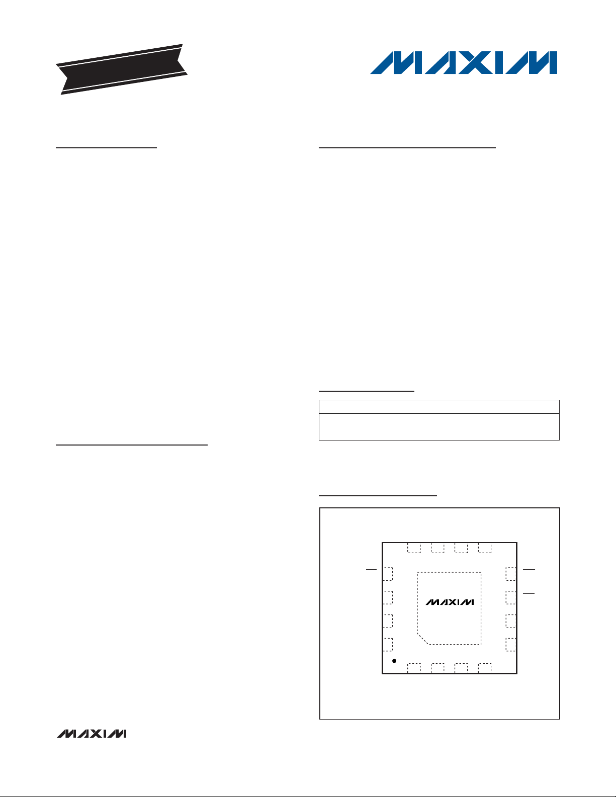
Pin Configuration
Ordering Information
19-3463; Rev 1; 2/10
For pricing, delivery, and ordering information, please contact Maxim Direct at 1-888-629-4642,
or visit Maxim’s website at www.maxim-ic.com.
EVALUATION KIT
AVAILABLE
*
EP = Exposed pad.
PART TEMP RANGE PIN-PACKAGE
MAX1564ETE -40°C to +85°C
16 Thin QFN-EP*
4mm x 4mm
TOP VIEW
OUTA
GND
OUTB
OUTC
9101112
INC
8
FLTC
7
FLTB
SETI
6
SEL
5
13
FLTA
ONC
14
15
ONB
16
ONA
12 4
INA
MAX1564
3
CC
INB
V
THIN QFN
4mm X 4mm
Page 2
MAX1564
Triple 1.2A USB Switch in 4mm x 4mm
Thin QFN
2 _______________________________________________________________________________________
ABSOLUTE MAXIMUM RATINGS
Stresses beyond those listed under “Absolute Maximum Ratings” may cause permanent damage to the device. These are stress ratings only, and functional
operation of the device at these or any other conditions beyond those indicated in the operational sections of the specifications is not implied. Exposure to
absolute maximum rating conditions for extended periods may affect device reliability.
IN_, ON_, OUT_, SEL, VCCto GND (Note 1)............-0.3V to +6V
FLT_, SETI to GND .....................................-0.3V to (V
CC
+ 0.3V)
IN_ to OUT_ (when disabled, Note 2) .........................-6V to +6V
IN_ to OUT_ (when enabled, Note 3)....................-1.5A to +2.3A
FLT_ Sink Current................................................................20mA
Continuous Power Dissipation
16-Pin 4mm x 4mm Thin QFN
(derate 16.9mW/°C above +70°C).............................1349mW
Operating Temperature Range ...........................-40°C to +85°C
Junction Temperature......................................................+150°C
Storage Temperature Range .............................-65°C to +150°C
Lead Temperature (soldering, 10s) ................................+300°C
ELECTRICAL CHARACTERISTICS
(V
IN_
= V
CC
= V
SEL
= V
ON_
= 5V, R
SETI
= 26.1kΩ, TA = -40°C to +85°C, unless otherwise noted. Typical values are at TA = +25°C.)
(Note 4)
Note 1: INA, INB, INC, and V
CC
must be connected together externally.
Note 2: Reverse current (current from OUT_ to IN_) is blocked when disabled.
Note 3: Forward and reverse current are internally limited.
PARAMETER CONDITIONS MIN TYP MAX UNITS
Supply Voltage Range 2.75 5.50 V
IN Standby Supply Current V
IN Quiescent Supply Current I
OUT_ Off-Leakage Current V
Undervoltage-Lockout Threshold V
Continuous Load Current 1.2 A
Current-Limit Threshold
Short-Circuit Current Limit
(Peak Amps)
Short-Circuit Current Limit
(RMS Amps)
Short-Circuit/Continuous CurrentLimit Transition Output Voltage
Threshold
V
= VCC = 5V, TA = +25°C 60
IN_
V
= VCC = 3V, TA = +25°C 80Switch On-Resistance
IN_
= VCC = 5V, TA = -40°C to +85°C 30 100
V
IN_
= 0V 3 7.5 µA
ON_
= 0A
OUT_
= 0V, V
ON_
rising, 3% hysteresis 2.2 2.5 2.7 V
IN_
R
= 26.1kΩ 1.20 1.37 1.54
SETI
R
= 39.2kΩ 0.79 0.91 1.03
SETI
= 60.4kΩ 0.49 0.59 0.68
R
SETI
= 0V
V
OUT_
= 0V
V
OUT_
= 0V 0.02 10 µA
OUT_
(Note 5) 1 V
V
= 5V,
ONA
V
= V
ONB
V
= V
ONA
V
= 0V
ONC
= V
V
ONA
R
= 26.1kΩ 1.46 1.8 2.20
SETI
R
= 39.2kΩ 1.2
SETI
R
= 60.4kΩ 0.77
SETI
R
= 26.1kΩ 0.55
SETI
R
= 39.2kΩ 0.37
SETI
= 60.4kΩ 0.23
R
SETI
ONC
ON0B
ONB
= 0V
= 5V,
= V
= 5V 60 120
ONC
40 80
55 100
mΩ
µA
A
A
A(RMS)
Page 3
MAX1564
Triple 1.2A USB Switch in 4mm x 4mm
Thin QFN
_______________________________________________________________________________________ 3
ELECTRICAL CHARACTERISTICS (continued)
(V
IN_
= V
CC
= V
SEL
= V
ON_
= 5V, R
SETI
= 26.1kΩ, TA = -40°C to +85°C, unless otherwise noted. Typical values are at TA = +25°C.)
(Note 4)
Note 4: Specifications to -40°C are guaranteed by design and characterization and not production tested.
Note 5: The output voltage at which the device transitions from short-circuit current limit to continuous current limit.
Current-Limit Fault-Blanking
Timeout Period
Turn-On Delay
Output Rise Time
Turn-Off Delay Time
Output Fall Time
Thermal Shutdown Threshold 10°C hysteresis +160 °C
Logic-Input High Voltage (ONA,
ONB, ONC, SEL)
Logic-Input Low Voltage (ONA,
ONB, ONC, SEL)
Logic-Input Current -1 +1 µA
FLT_ Output Low Voltage I
FLT_ Output High Leakage
Current
SETI Output Voltage 600 mV
SETI External Resistor Range 26.1kΩ sets 1.37A maximum current limit 26 60 kΩ
OUT_ Auto-Restart Current In latched-off state, V
OUT_ Auto-Restart Threshold In latched-off state, V
OUT_ Auto-Restart Delay Time In latched-off state, V
Reverse Current Detection
Threshold
Reverse Current Detection Blank
Time
PARAMETER CONDITIONS MIN TYP MAX UNITS
From current-limit condition to FLT_ low 10 20 40 ms
= 10Ω, C
R
OUT _
measured from ON_ high to 10% of V
= 10Ω, C
R
OUT_
of V
OUT_
R
= 10Ω, C
OUT_
90% of V
R
of V
V
V
V
V
SINK
V
OUT_
= 10Ω, C
OUT_
OUT_
= 2.7V to 4.0V 1.6
IN_
= 4.0V to 5.5V 2.0
IN_
= 2.7V to 4.0V 0.6
IN_
= 4.0V to 5.5V 0.8
IN_
= 1mA 0.4 V
= 5.5V 1 µA
FLT_
= 1µF,
OUT_
OUT_
_= 1µF, measured from 10% to 90%
OUT
= 1µF, measured from ON_ low to
OUT_
= 1µF, measured from 90% to 10%
OUT_
= 0V 10 25 50 mA
OUT_
rising 0.4 0.5 0.6 V
OUT_
> 1V 10 20 40 ms
OUT_
0.5 1.5 4.0 ms
3.5 ms
100 1000 µs
4.0 ms
0.9 A
10 20 40 ms
V
V
Page 4
MAX1564
Triple 1.2A USB Switch in 4mm x 4mm
Thin QFN
4 ________________________________________________________________________________________
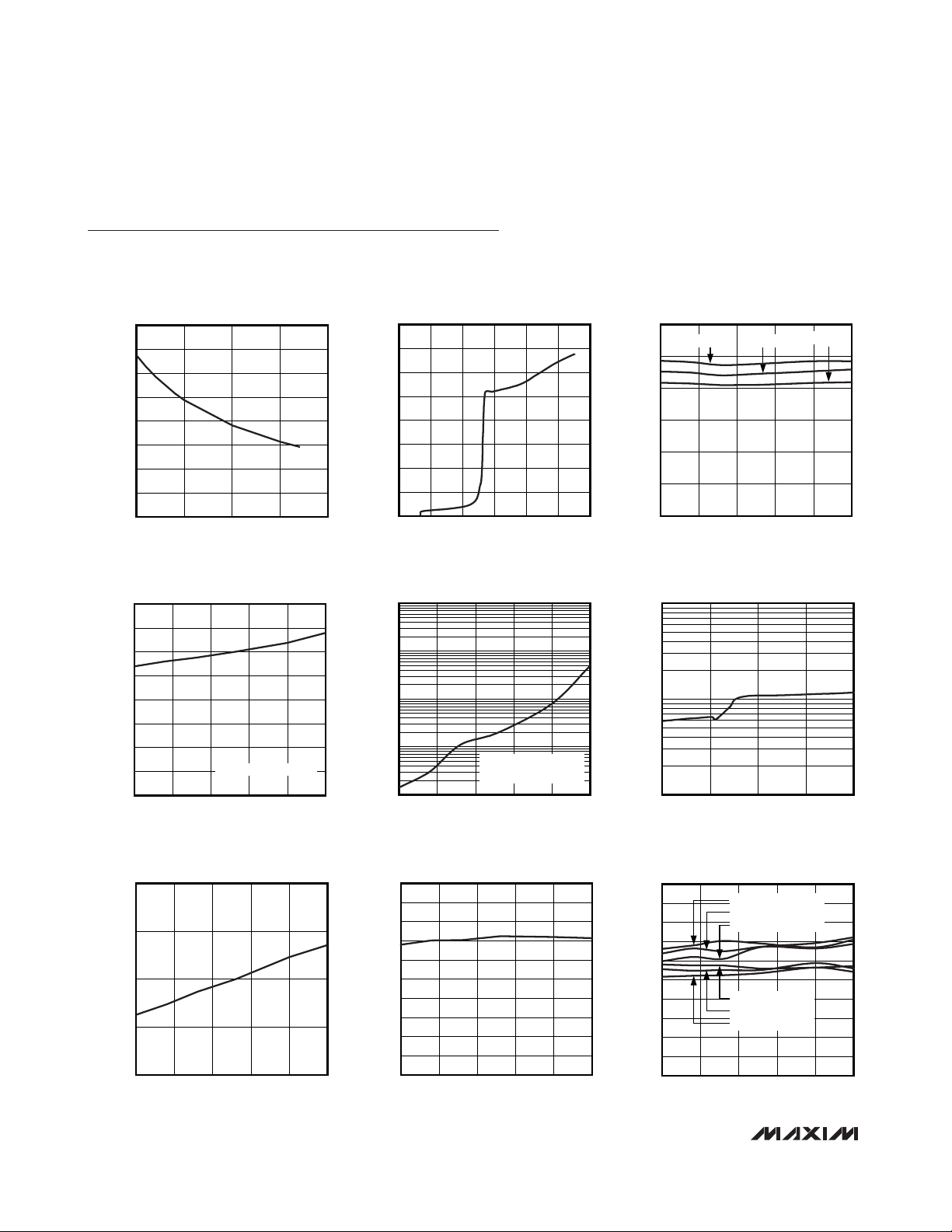
Typical Operating Characteristics
(Circuit of Figure 1, V
INA
= V
INB
= V
INC
= V
SEL
= V
ONA
= V
ONB
= V
ONC
= 5V, TA = +25°C, unless otherwise noted.)
CURRENT LIMIT vs. R
SETI
MAX1564 toc01
R
SETI
(kΩ)
CURRENT LIMIT (A)
6636 46 56
0.2
0.4
0.6
0.8
1.0
1.2
1.4
1.6
0
26
QUIESCENT SUPPLY CURRENT
vs. INPUT VOLTAGE
MAX1564 toc02
INPUT VOLTAGE (V)
INPUT CURRENT (µA)
541 2 3
10
20
30
40
50
60
70
80
0
06
TEMPERATURE (°C)
603510-15
30
40
50
60
70
80
20
-40 85
QUIESCENT SUPPLY CURRENT
vs. TEMPERATURE
MAX1564 toc03
INPUT CURRENT (µA)
VIN = 5.5V
VIN = 4.5V
VIN = 5V
STANDBY CURRENT vs. TEMPERATURE
MAX1564 toc04
TEMPERATURE (°C)
INPUT CURRENT (µA)
6035-15 10
0.5
1.0
1.5
2.0
3.0
2.5
3.5
4.0
0
-40 85
V
ONA
= V
ONB
= V
ONC
= 0V
SWITCH OFF LEAKAGE CURRENT
vs. TEMPERATURE
MAX1564 toc05
TEMPERATURE (°C)
LEAKAGE CURRENT (µA)
603510-15
0.01
0.1
1
10
0.001
-40 85
V
ONA
= V
ONB
= V
ONC
= 0V
V
OUT
= 0V
REVERSE BLOCK LEAKAGE CURRENT
vs. OUTPUT VOLTAGE
MAX1564 toc06
OUPUT VOLTAGE (V)
LEAKAGE CURRENT (µA)
4.84.13.4
10
2.7
5.5
100
1
NORMALIZED ON-RESISTANCE
vs. TEMPERATURE
MAX1564 toc07
TEMPERATURE (°C)
NORMALIZED R
ON
603510-15
0.75
1.00
1.25
1.50
0.50
-40 85
CONTINUOUS CURRENT LIMIT
vs. TEMPERATURE
MAX1564 toc08
TEMPERATURE (°C)
CURRENT LIMIT (A)
603510-15
1.05
1.10
1.15
1.20
1.25
1.30
1.35
1.40
1.45
1.50
1.00
-40 85
OUTPUT RISE TIME vs. TEMPERATURE
OUTPUT RISE TIME (ms)
1
2
3
4
5
6
7
8
9
10
0
MAX1564 toc09
TEMPERATURE (°C)
603510-15-40 85
VIN = 5.5V, R
LOAD
= 5Ω
V
IN
= 5V, R
LOAD
= 5Ω
V
IN
= 4.5V, R
LOAD
= 5Ω
VIN = 5V, NO LOAD
V
IN
= 5.5V, NO LOAD
V
IN
= 4.5V, NO LOAD
Page 5

MAX1564
Triple 1.2A USB Switch in 4mm x 4mm
Thin QFN
_______________________________________________________________________________________ 5
Typical Operating Characteristics (continued)
(Circuit of Figure 1, V
INA
= V
INB
= V
INC
= V
SEL
= V
ONA
= V
ONB
= V
ONC
= 5V, TA = +25°C, unless otherwise noted.)
OUTPUT FALL TIME vs. TEMPERATURE
OUTPUT FALL TIME (ms)
2.2
2.4
2.6
2.8
3.0
3.2
3.4
3.6
3.8
4.0
2.0
MAX1564 toc10
TEMPERATURE (°C)
603510-15-40 85
R
LOAD
= 5Ω
VIN = 5VVIN = 5.5V VIN = 4.5V
FAULT-BLANKING TIME (ms)
18
19
20
21
23
22
24
25
17
FAULT-BLANKING TIME vs. TEMPERATURE
MAX1564 toc11
TEMPERATURE (°C)
603510-15-40 85
VIN = 5V
VIN = 5.5V
VIN = 4.5V
AUTO-RESTART CURRENT vs. TEMPERATURE
MAX1564 toc13
AUTO-RESTART CURRENT (mA)
5
10
15
20
30
25
35
40
0
TEMPERATURE (°C)
603510-15-40 85
VIN = 5V
VIN = 5.5V
VIN = 4.5V
4.84.13.42.7 5.5
AUTO-RESTART CURRENT vs. INPUT VOLTAGE
MAX1564 toc14
INPUT VOLTAGE (V)
AUTO-RESTART CURRENT (mA)
16
18
20
22
24
26
28
14
TA = +85°C
TA = +25°C
TA = -40°C
FLT_ LOW VOLTAGE vs. TEMPERATURE
V
FLT_
(mV)
125
175
225
275
75
MAX1564 toc12
TEMPERATURE (°C)
603510-15-40 85
R
PULLUP
= 5kΩ
VIN = 5V
VIN = 5.5V
VIN = 4.5V
Page 6

MAX1564
Triple 1.2A USB Switch in 4mm x 4mm
Thin QFN
6 _______________________________________________________________________________________
Typical Operating Characteristics (continued)
(Circuit of Figure 1, V
INA
= V
INB
= V
INC
= V
SEL
= V
ONA
= V
ONB
= V
ONC
= 5V, TA = +25°C, unless otherwise noted.)
OVERLOAD RESPONSE INTO 2.5Ω
I
OUT_
V
OUT_
(AC-COUPLED)
V
FLT_
V
IN
4ms/div
SWITCH TURN-ON TIME
MAX1564 toc15
MAX1564 toc17
1A/div
2V/div
100mV/div
5V/div
SHORT-CIRCUIT RESPONSE INTO 0Ω
V
FLT_
V
OUT_
V
I
OUT_
IN
(AC-COUPLED)
SWITCH TURN-OFF TIME
MAX1564 toc16
5V/div
5V/div
200mV/div
1A/div
10ms/div
MAX1564 toc18
2V/div
V
OUT_
V
ON_
1ms/div
1V/div
R
= 5Ω
LOAD
V
OUT_
V
ON_
R
LOAD
= 5Ω
1ms/div
2V/div
1V/div
Page 7

MAX1564
Triple 1.2A USB Switch in 4mm x 4mm
Thin QFN
_______________________________________________________________________________________ 7
Detailed Description
Undervoltage Lockout (UVLO) and Input
Voltage Requirements
The MAX1564 includes undervoltage-lockout (UVLO)
circuitry to prevent erroneous switch operation when
the input voltage is low during startup and brownout
conditions. The IC is disabled when the input voltage is
less than 2.5V (typ). FLT_ asserts low during a UVLO
condition.
Current-Limit Fault Protection
The MAX1564 uses two methods to protect the circuit
from overcurrent conditions. During an overcurrent
event, the IC senses the switch output voltage and
selects either continuous current limiting or short-circuit
Pin Description
PIN NAME FUNCTION
Input Power Supply for OUTA. Provides power to OUTA. INA, INB, INC, and V
1 INA
2V
3 INB
4INC
5 SEL
6 SETI
7 FLTB
8 FLTC
9 OUTC Power Output for Switch C. OUTC is high impedance during shutdown.
10 OUTB Power Output for Switch B. OUTB is high impedance during shutdown.
11 GND Ground. Connect ground to the exposed pad directly under the IC.
12 OUTA Power Output for Switch A. OUTA is high impedance during shutdown.
13 FLTA
CC
together externally. Bypass with a 0.1µF capacitor to GND. Additional capacitors can be used as
required.
Input Power Supply for the MAX1564. Provides power to the IC. INA, INB, INC, and VCC must be
connected together externally.
Input Power Supply for OUTB. Provides power to OUTB. INA, INB, INC, and V
together externally.
Input Power Supply for OUTC. Provides power to OUTC. INA, INB, INC, and V
together externally.
Polarity Control Input. Selects the polarity of ONA, ONB, and ONC. Connect to V
ON_ inputs. Connect to GND for active-low ON_ inputs.
Current-Limit Program Input. Connect a resistor from SETI to GND in the 26kΩ to 60kΩ range. I
1.37A x 26.1kΩ / R
Fault-Indicator Output for Switch B. FLTB is an open-drain output that goes low when INB is below the
UVLO threshold, or when switch B is in current limit for greater than 20ms, or when switch B is in
thermal shutdown.
Fault Indicator Output for Switch C. FLTC is an open-drain output that goes low when INC is below the
UVLO threshold, or when switch C is in current limit for greater than 20ms, or when switch C is in
thermal shutdown.
Fault Indicator Output for Switch A. FLTA is an open-drain output that goes low when INA is below the
UVLO threshold, or when switch A is in current limit for greater than 20ms, or when switch A is in
thermal shutdown.
SETI
.
must be connected
CC
must be connected
CC
must be connected
CC
for active-high
CC
=
LIM
14 ONC
15 ONB
16 ONA
— EP Exposed Pad. Connect exposed pad to a large ground plane to improve thermal power dissipation.
Control Input for Switch C. ONC is active high when SEL is connected to V
SEL is connected to GND.
Control Input for Switch B. ONB is active high when SEL is connected to V
SEL is connected to GND.
Control Input for Switch A. ONA is active high when SEL is connected to V
SEL is connected to GND.
and active low when
CC
and active low when
CC
and active low when
CC
Page 8

MAX1564
Triple 1.2A USB Switch in 4mm x 4mm
Thin QFN
8 _______________________________________________________________________________________
current limiting. When V
OUT_
is greater than 1V, the
device operates in continuous current-limit mode and
limits output current to a user-programmable level.
When V
OUT_
is less than 1V, the device operates in
short-circuit current-limit mode and pulses the output
current to levels that are 30% (typ) higher than the
selected current limit. When either fault condition persists for 20ms (typ), the output turns off and its fault flag
is asserted. The output automatically restarts 20ms
after the short or overload is removed.
Auto-Restart Mode
The MAX1564 detects short-circuit removal by sourcing
25mA from the output and monitoring the output voltage. When the voltage at the output exceeds 0.5V for
20ms, the fault flag resets, the output turns back on,
and the 25mA current source turns off. Active loads are
not expected to draw measurable current when supplied with less than 0.5V. The MAX1564 can also be
reset from a fault by toggling the ON_ input for the
offending channel.
Reverse Current Blocking
The USB specification does not allow an output device
to source current back into the USB port. However, the
MAX1564 is designed to safely power noncompliant
devices. During normal operation with the channel
enabled, the IC immediately turns off the switch if the
output voltage rises above the input voltage sufficiently
to create a reverse current in excess of 0.9A (typ). If the
output voltage condition persists for longer than 20ms
(typ), the switch remains off and the FLT_ flag is asserted. When any channel is disabled, the output is
switched to a high-impedance state, blocking reverse
current flow from the output back to the input.
Thermal Shutdown
Independent thermal shutdown of each channel permits delivering power to normal loads even if one load
has a fault condition. The thermal limit does not have
the 20ms fault blanking but sets the same fault latch
that is used for other faults. Exiting this latched state is
described in the
Auto-Restart Mode
section.
Fault Indicators and Fault Blanking
The MAX1564 provides an independent open-drain
fault output (FLT_) for each switch. Connect FLT_ to IN_
through a 100kΩ pullup resistor for most applications.
FLT_ asserts low when any of the following conditions
occur:
• The input voltage is below the UVLO threshold.
• The switch junction temperature exceeds the +160°C
thermal-shutdown temperature limit.
• The switch is in current-limit or short-circuit currentlimit mode after the fault-blanking period (20ms typ)
expires.
• The reverse current condition exists after the faultblanking period expires.
The FLT_ output goes high impedance after a 20ms
delay once the fault condition is removed. Ensure that
the MAX1564 input bypass capacitance prevents
glitches from triggering the FLT_ outputs. To differentiate large capacitive loads from short circuits or sustained overloads, the MAX1564 has an independent
fault-blanking circuit for each switch. When a load transient causes the output to enter current limit, an internal
counter monitors the duration of the fault. For load
faults exceeding the 20ms fault-blanking time, the
switch turns off, FLT_ asserts low, and the output enters
auto-restart mode (see the
Current-Limit Fault
Protection
and
Auto-Restart Mode
sections). Only current-limit and short-circuit faults are blanked. Thermaloverload faults and input voltages below the UVLO
threshold immediately turn off the offending output and
assert FLT_ low.
Fault blanking allows the MAX1564 to handle USB
loads that might not be fully compliant with USB
specifications. The MAX1564 successfully powers USB
Figure 1. Typical Application Circuit
R2
100kΩ
INPUT
2.75V TO 5.5V
SELECT INPUT
C1
0.1µF
ACTIVE-HIGH/
ACTIVE-LOW
26.1kΩ
1
INA
3
MAX1564
INB
4
INC
2
V
CC
5
SEL
16
ONA
15
ONB
14
ONC
6
SETI
GND
R1
13
FLTA
R3
C2
1µF
C3
1µF
C4
1µF
100kΩ
100kΩ
R4
USB
PORT A
USB
PORT B
USB
PORT C
7
FLTB
8
FLTC
12
OUTA
10
OUTB
9
OUTC
11
Page 9

MAX1564
Triple 1.2A USB Switch in 4mm x 4mm
Thin QFN
_______________________________________________________________________________________ 9
loads with additional bypass capacitance and/or large
startup currents while protecting the upstream power
source. No fault is reported if the output voltage rises
nominal within the 20ms blanking period.
Applications Information
Setting the Current Limit
The current limit for the MAX1564 is user programmable using the SETI input. Connect a resistor from SETI
to GND (R1) to set the current limit. The value for R1 is
calculated as:
I
LIMIT
= 1.37A x 26.1kΩ / R1
R1 must be between 26kΩ and 60kΩ.
Input Capacitor
To limit the input voltage drop during momentary output
load transients, connect a capacitor from IN_ to
ground. A 0.1µF ceramic capacitor is required for local
decoupling; however, higher capacitor values further
reduce the voltage drop at the input. When driving
inductive loads, a larger capacitance prevents voltage
spikes from exceeding the MAX1564’s absolute maximum ratings.
Output Capacitor
A capacitor as large as 2000µF may be used on the
output to smooth out transients and/or increase rise/fall
times. Larger output capacitance may be used, but the
resulting output charge time during startup may exceed
the fault blanking period, resulting in a FLT_ flag.
Driving Inductive Loads
A wide variety of devices (mice, keyboards, cameras,
and printers) typically connect to the USB port with
cables, adding an inductive component to the load. This
inductance causes the output voltage at the USB port to
oscillate during a load step. The MAX1564 drives inductive loads; however, care must be taken to avoid
exceeding the device’s absolute maximum ratings.
Usually, the load inductance is relatively small, and the
MAX1564’s input includes a substantial bulk capacitance from an upstream regulator, as well as local
bypass capacitors, limiting overshoot. If severe ringing
occurs because of large load inductance, clamp the
MAX1564 outputs below +6V and above -0.3V.
Turn-On and Turn-Off Behavior
Slow turn-on and turn-off under normal operating conditions minimizes loading transients on the upstream
power source. Rapid turn-off under fault conditions
(thermal, short circuit, and UVLO) is done for maximum
safety.
SEL sets the active polarity of the logic inputs of the
MAX1564. Connect ON_ to the same voltage as SEL to
enable the respective OUT_ switch. Connect ON_ to
the opposite voltage as SEL to disable the respective
output (see Table 1). The output of a disabled switch
enters a high-impedance state.
Layout and Thermal Dissipation
Keep all input/output traces as short as possible to
reduce the effect of undesirable parasitic inductance
and optimize the switch response time to output shortcircuit conditions. Place input and output capacitors no
more than 5mm from device leads. Connect IN_ and
OUT_ to the power bus with short traces. Wide power
bus planes at IN_ and OUT_ provide superior heat dissipation as well. An active switch dissipates little power
with minimal change in package temperature. Calculate
the power dissipation for this condition as follows:
P = I
OUT_
2
x R
ON
At the normal operating current (I
OUT_
= 0.5A) and the
maximum on-resistance of the switch (100mΩ), the
power dissipation is:
P = (0.5A)2x 0.100Ω = 25mW per switch
The worst-case power dissipation occurs when the output current is just below the current-limit threshold with
an output voltage greater than 1V. In this case, the
power dissipated in each switch is the voltage drop
across the switch multiplied by the current limit:
P = I
LIM
x (VIN- V
OUT
)
For a 5.5V input and 1V output, the maximum power
dissipation per switch is:
P = 1.54A x (5.5V - 1V) = 6.9W
Because the package power dissipation is 1349mW,
the MAX1564 die temperature may exceed the +160°C
thermal-shutdown threshold, in which case the switch
output shuts down until the junction temperature cools
by 10°C. In a continuous overload condition, this causes a cyclical on/off situation. The duty cycle and period
of this situation are strong functions of the ambient temperature and the PC board layout (see the
Thermal
Shutdown
section).
Table 1. SEL/ON_ Inputs
SEL ON_ OUT_ STATE
High High Enabled
High Low Disabled
Low High Disabled
Low Low Enabled
Page 10

MAX1564
Triple 1.2A USB Switch in 4mm x 4mm
Thin QFN
10 ______________________________________________________________________________________
If the output current exceeds the current-limit threshold,
or the output voltage is pulled below the short-circuit
detect threshold, the MAX1564 enters a fault state after
20ms, at which point auto-restart mode is enabled and
25mA is sourced by the output. For a 5V input, OUT_
short circuited to GND, and auto-restart mode active,
the power dissipation is as follows:
P = 0.025A x 5V = 0.125W
PACKAGE TYPE PACKAGE CODE DOCUMENT NO.
16 TQFN-EP T1644-4
21-0139
Package Information
For the latest package outline information and land patterns, go
to www.maxim-ic.com/packages
. Note that a “+”, “#”, or “-” in
the package code indicates RoHS status only. Package drawings may show a different suffix character, but the drawing pertains to the package regardless of RoHS status.
Chip Information
PROCESS: BiCMOS
Page 11

MAX1564
Triple 1.2A USB Switch in 4mm x 4mm
Thin QFN
Maxim cannot assume responsibility for use of any circuitry other than circuitry entirely embodied in a Maxim product. No circuit patent licenses are
implied. Maxim reserves the right to change the circuitry and specifications without notice at any time.
Maxim Integrated Products, 120 San Gabriel Drive, Sunnyvale, CA 94086 408-737-7600 ____________________
11
© 2010 Maxim Integrated Products Maxim is a registered trademark of Maxim Integrated Products, Inc.
Revision History
REVISION
NUMBER
0 4/01 Initial release —
1 2/10 Removed UL Certification Pending bullet from Features section 1
REVISION
DATE
DESCRIPTION
PAGES
CHANGED
 Loading...