

Page 1
For pricing, delivery, and ordering information, please contact Maxim Direct at 1-888-629-4642,
or visit Maxim's website at www.maxim-ic.com.
General Description
The MAX1558/MAX1558H are dual, current-limited
switches with autoreset for USB applications. Autoreset
latches the switch off if it is shorted for more than 20ms,
saving system power. The shorted output is then tested
to determine when the short is removed to automatically
restart the channel. Each channel delivers up to 1.2A
and meets all IEC specifications for USB ports. Low
quiescent supply current (45µA) and standby current
(3µA) conserve battery power in portable applications.
The MAX1558/MAX1558H safety features ensure that the
USB port is protected. Built-in thermal-overload protection
limits power dissipation and junction temperature.
Accurate, programmable current-limiting circuitry protects the input supply against both overload and short-circuit conditions. 20ms fault blanking enables the circuit to
ignore transient faults, such as those caused when hot
swapping a capacitive load, preventing false alarms to
the host system. The MAX1558/MAX1558H also feature
reverse-current protection circuitry to block current flow
from the output to the input when the switches are off.
The MAX1558/MAX1558H are available in space-saving 3mm x 3mm, 10-pin TDFN packages. The MAX1558
is enabled with an active-low signal, and the
MAX1558H is enabled with an active-high signal.
Applications
USB Ports and Hubs
Notebook Computers and Desktops
PDAs and Palmtop Computers
Docking Stations
Features
♦ 55mΩ Switch Resistance
♦ Tiny 10-Pin, 3mm x 3mm TDFN Package
♦ 14% Accurate Current Limit
♦ Autorestart when Fault is Removed
♦ Programmable Current Up to 1.2A
♦ Thermal-Overload Protection
♦ Built-In 20ms Fault Blanking
♦ Compliant to All USB Specifications
♦ 2.7V to 5.5V Supply Range
♦ Independent-Output Fault Indicators
♦ Block Reverse Current when Disabled
♦ 15kV ESD Protection (with Capacitor)
♦ UL Recognized: UL# E211395
MAX1558/MAX1558H
Dual, 3mm x 3mm, 1.2A/Programmable-Current
USB Switches with Autoreset
________________________________________________________________
Maxim Integrated Products
1
Ordering Information
19-3128; Rev 2; 3/08
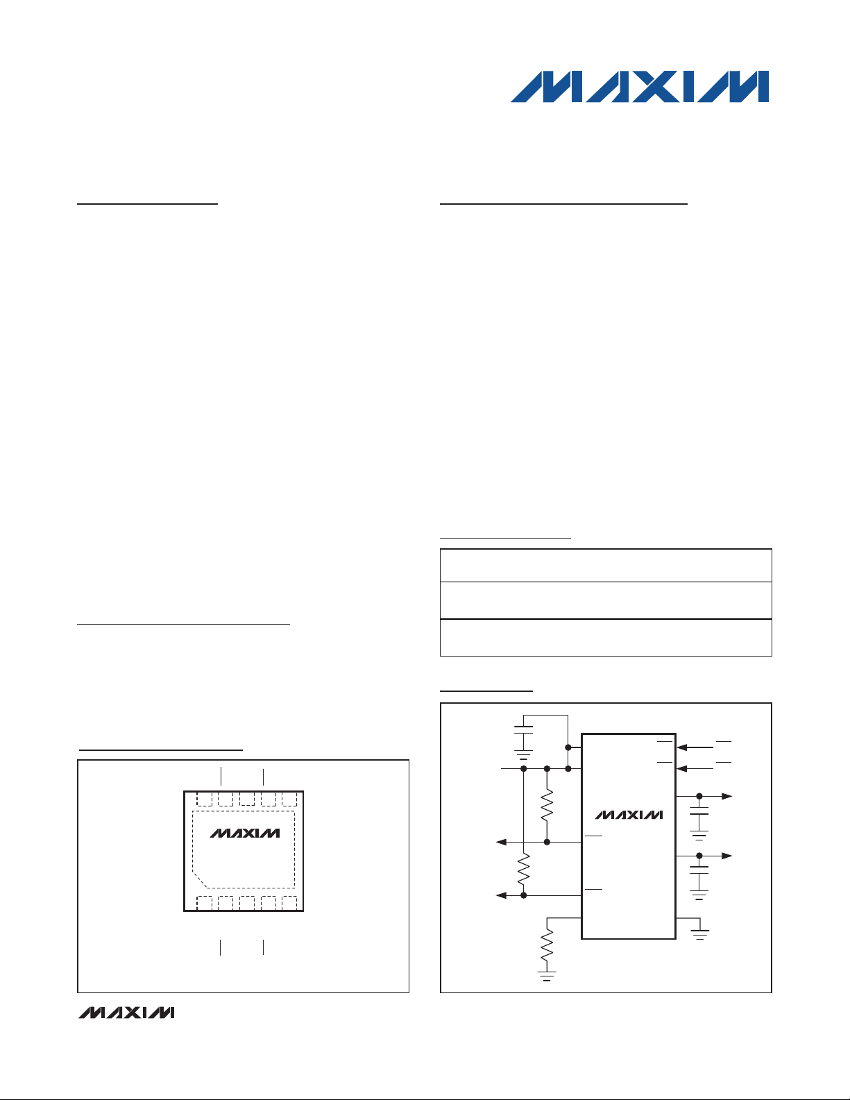
Typical Operating Circuit
Pin Configuration
+
Denotes a lead-free package.
PART TEMP RANGE
MAX1558ETB+ -40°C to +85°C
MAX1558HETB+ -40°C to +85°C
PINPACKAGE
10 TDFN
(3mm x 3mm)
10 TDFN
(3mm x 3mm)
TOP
MARK
AAR
AAS
TOP VIEW
OUTA
10
+
1
INA
GND
FLTA
98
MAX1558
(MAX1558H)
23
3mm x 3mm
76
45
ISET
ONA (ONA)
TDFN
OUTB
FLTB
INB
ONB (ONB)
INPUT
2.7V TO 5.5V
INA
INB
MAX1558
FLTA
FLTB
ISET
ONA
ONB
OUTA
OUTB
GND
ONA
ONB
USB
PORT A
USB
PORT B
Page 2
MAX1558/MAX1558H
Dual, 3mm x 3mm, 1.2A/Programmable-Current
USB Switches with Autoreset
2 _______________________________________________________________________________________
ABSOLUTE MAXIMUM RATINGS
ELECTRICAL CHARACTERISTICS
(V
INA
= V
INB
= 5V, V
ONA
= V
ONB
= 0V (MAX1558), V
ONA
= V
ONB
= 5V (MAX1558H), R
ISET
= 26kΩ to GND, TA= 0°C to +85°C,
unless otherwise noted. Typical values are at T
A
= +25°C.) (Note 3)
Stresses beyond those listed under “Absolute Maximum Ratings” may cause permanent damage to the device. These are stress ratings only, and functional
operation of the device at these or any other conditions beyond those indicated in the operational sections of the specifications is not implied. Exposure to
absolute maximum rating conditions for extended periods may affect device reliability.
IN_, ON_, OUT_, ISET, FLT_ to GND........................-0.3V to +6V
IN_ to OUT_ (when disabled) (Note 1) ........................-6V to +6V
IN_ to OUT_ (when enabled) (Note 2)............-1.6A to +1.6A
RMS
FLT_ Sink Current................................................................20mA
Continuous Power Dissipation (T
A
= +70°C)
10-Pin TDFN 3mm x 3mm
(derate 24.4mW/°C above +70°C).............................1952mW
Operating Temperature Range ...........................-40°C to +85°C
Junction Temperature......................................................+160°C
Storage Temperature Range .............................-65°C to +150°C
Lead Temperature (soldering, 10s) .................................+300°C
(
)
Note 1: Reverse current (current from OUT_ to IN_) is blocked when disabled.
Note 2: Forward current (current from IN_ to OUT_) is internally limited. Reverse current, from OUT_ to IN_, is not limited when the
device is enabled and must be kept below 1.5A
RMS
to prevent permanent device damage. When the MAX1558/MAX1558H
are disabled, the switch turns off and reverse current is internally blocked.
PARAMETER SYMBOL CONDITIONS MIN TYP MAX UNITS
Supply Voltage Range 2.75 5.50 V
Standby Supply Current Both switches disabled 3 6 µA
Quiescent Supply Current Both switches enabled 45 75 µA
OUT_ Off-Leakage Current Switches disabled
Reverse Leakage Current
Undervoltage-Lockout Threshold V
Continuous Load Current R
RMS Short-Circuit Current Limit I
Short-Circuit Continuous CurrentLimit Transition Threshold
Fault-Blanking Timeout Period From I
Turn-On Delay t
SHORT
SHORT
V
ON
V
V
V
switches disabled
UVLO
Rising edge, 3% hysteresis 2.3 2.5 2.7 V
V
0.5V
V
(I
V
(I
(Note 4) 1 V
R
ON
include rise time (from ON asserted to
V
= 5V, TA = +25°C5575
IN_
= 3.3V, TA = +25°C64Switch On-Resistance R
IN_
= 4.4V, TA = 0°C to +85°C 105
IN_
= 0V, V
IN_
= 26kΩ 1.2 A
ISET
- V
IN_
= 0V
OUT_
pulsing)
OUT_
= 0V
OUT_
pulsing)
OUT_
LIMIT
= 10Ω, C
OUT_
= 10% V
OUT_
V
OUTA
V
OUTA
= V
OUT_
OUTA
=
OUTB
R
ISET
R
ISET
R
ISET
R
ISET
R
ISET
R
ISET
R
ISET
R
ISET
R
ISET
condition to 50% of V
= 1µF, does not
OUT_
)
IN_
= V
= V
= 0V 0.03 10
OUTB
= 5V 0.03
OUTB
= 5V, both
= 26kΩ 1.20 1.4 1.60
= 39kΩ 0.80 0.925 1.05Current-Limit Threshold
= 60kΩ 0.50 0.6 0.70
= 26kΩ 1.45 2.0 2.60
= 39kΩ 1.40Peak Short-Circuit Current Limit I
= 60kΩ 0.90
= 26kΩ 0.55
= 39kΩ 0.37
= 60kΩ 0.23
FLT_
0.03 µA
82040ms
0.5 1.4 4.0 ms
A
mΩ
µA
PEAK
A
RMS
A
Page 3
MAX1558/MAX1558H
Dual, 3mm x 3mm, 1.2A/Programmable-Current
USB Switches with Autoreset
_______________________________________________________________________________________ 3
ELECTRICAL CHARACTERISTICS (continued)
(V
INA
= V
INB
= 5V, V
ONA
= V
ONB
= 0V (MAX1558), V
ONA
= V
ONB
= 5V (MAX1558H), R
ISET
= 26kΩ to GND, TA= 0°C to +85°C,
unless otherwise noted. Typical values are at T
A
= +25°C.) (Note 3)
ELECTRICAL CHARACTERISTICS
(V
INA
= V
INB
= 5V, V
ONA
= V
ONB
= 0V (MAX1558), V
ONA
= V
ONB
= 5V (MAX1558H), R
ISET
= 26kΩ to GND, TA= -40°C to +85°C,
unless otherwise noted.)
(
)
PARAMETER SYMBOL CONDITIONS MIN TYP MAX UNITS
Output Rise Time t
Turn-Off Delay from ON t
Output Fall Time t
Thermal-Shutdown Threshold 10°C hysteresis +160 °C
ONA/ONB Logic Input High
Voltage
ONA/ONB Logic Input Low
Voltage
Logic Input Current V
FLT_ Output Low Voltage I
FLT_ Output High Leakage
Current
Autorestart Current In latched-off state, V
Autorestart Threshold In latched-off state, rising 0.4 0.5 0.6 V
Autorestart Delay In latched-off state, V
RISE
C
90% of V
R
OFF
include rise time (from ON deasserted to
V
FALL
V
V
C
10% of V
V
IH
V
V
IL
V
V
OUT_
OUT_
= 1µF, R
= 10Ω, C
= 10Ω, (from 10% to
OUT_
)
OUT_
= 1µF, does not
OUT_
4ms
100 1000 µs
= 90% V
OUT_
= 1µF, R
OUT_
OUT_
= 2.7V to 4.0V 1.6
IN_
= 4.0V to 5.5V 2.0
IN_
= 2.7V to 4.0V 0.6
IN_
= 4.0V to 5.5V 0.8
IN_
= 0V or V
ON_
= 1mA 0.4 V
SINK
= V
IN_
FLT_
)
IN_
= 10Ω (from 90% to
)
OUT_
IN_
-1 +1 µA
3ms
= 5.5V 1 µA
= 0V 10 25 50 mA
OUT_
> 1V 8 20 40 ms
OUT_
V
V
PARAMETER SYMBOL CONDITIONS MIN TYP MAX UNITS
Supply Voltage Range 2.7 5.5 V
Switch On-Resistance R
Standby Supply Current Both switches disabled 6 µA
Quiescent Supply Current Both switches enabled 75 µA
OUT_ Off-Leakage Current Switches disabled, V
Undervoltage-Lockout Threshold V
Continuous Load Current R
Current-Limit Threshold V
Peak Short-Circuit Current Limit I
Fault-Blanking Timeout Period From I
SHORT
ON
UVLO
V
= 5V, TA = +25°C75
IN_
V
= 4.4V, TA = 0°C to +85°C 105
IN_
OUTA
= V
= 0V 10 µA
OUTB
Rising edge, 3% hysteresis 2.3 2.7 V
= 26kΩ 1.2 A
ISET
R
= 26kΩ 1.20 1.60
ISET
V
(I
IN_
OUT_
OUT_
- V
= 0.5V
OUT_
= 0V
pulsing)
condition to 50% of V
LIMIT
R
= 39kΩ 0.80 1.05
ISET
= 60kΩ 0.50 0.70
R
ISET
R
= 26kΩ 1.45 2.60 A
ISET
FLT_
840ms
mΩ
A
PEAK
Page 4
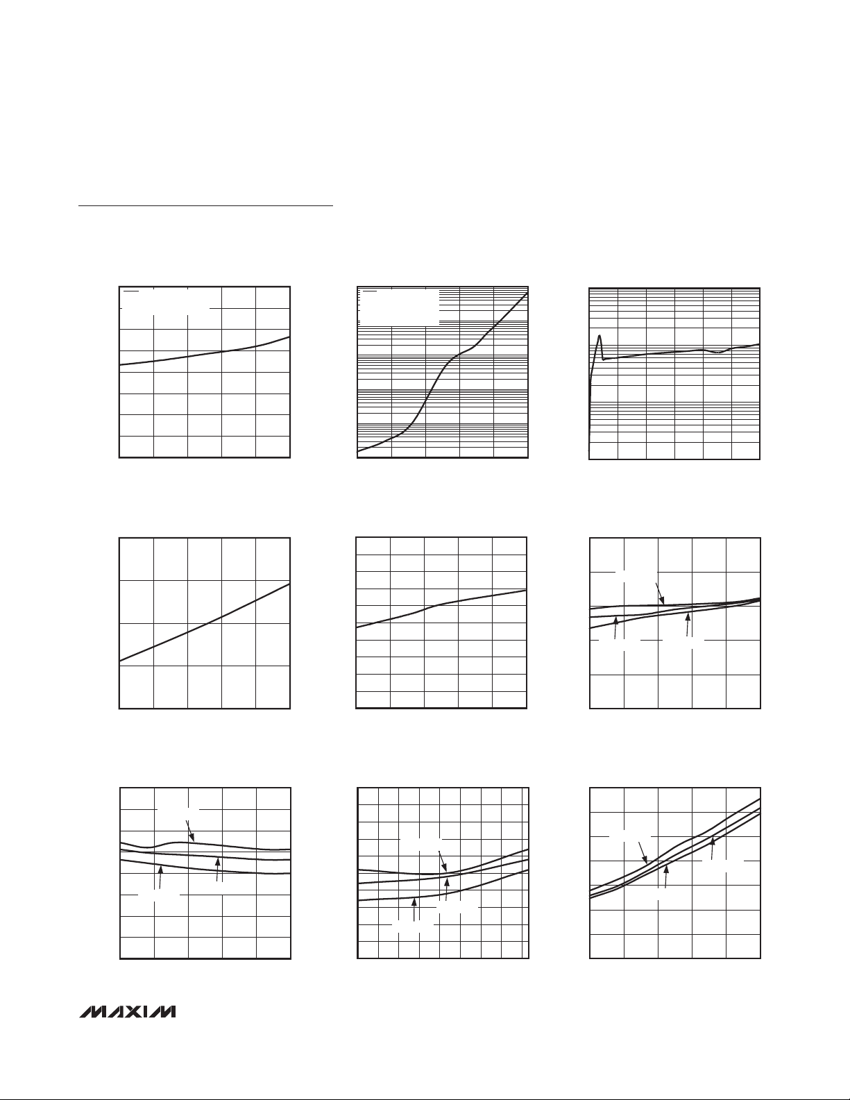
Typical Operating Characteristics
(V
INA
= V
INB
= 5V, V
ONA
= V
ONB
= 0V (MAX1558), V
ONA
= V
ONB
= 5V (MAX1558H), R
ISET
= 26kΩ to GND. Typical values are at TA=
+25°C, unless otherwise noted.)
MAX1558/MAX1558H
Dual, 3mm x 3mm, 1.2A/Programmable-Current
USB Switches with Autoreset
4 _______________________________________________________________________________________
ELECTRICAL CHARACTERISTICS (continued)
(V
INA
= V
INB
= 5V, V
ONA
= V
ONB
= 0V (MAX1558), V
ONA
= V
ONB
= 5V (MAX1558H), R
ISET
= 26kΩ to GND, TA= -40°C to +85°C,
unless otherwise noted.)
Note 3: Specifications from 0°C to -40°C are guaranteed by design but not 100% tested.
Note 4: The output voltage at which the device transitions from short-circuit current limit to continuous current limit. See the
Output-
Current Fault Protection
section.
PARAMETER SYMBOL CONDITIONS MIN TYP MAX UNITS
Turn-On Delay t
Turn-Off Delay from ON t
ONA/ONB Logic Input High
Voltage
ONA/ONB Logic Input Low
Voltage
Logic Input Current V
FLT_ Output Low Voltage I
FLT_ Output High Leakage
Current
Autorestart Current In latched-off state, V
Autorestart Threshold In latched-off state, rising 0.4 0.6 V
Autorestart Delay In latched-off state, V
ON
OFF
V
V
R
OUT_
= 10Ω, C
= 1µF, does not
OUT_
include rise time (from ON asserted to
V
R
OUT_
OUT_
= 10% V
= 10Ω, C
)
IN_
= 1µF, does not
OUT_
include rise time (from ON deasserted to
V
= 90% V
OUT_
V
= 2.7V to 4.0V 1.6
IH
IL
IN_
V
= 4.0V to 5.5V 2.0
IN_
V
= 2.7V to 4.0V 0.6
IN_
V
= 4.0V to 5.5V 0.8
IN_
= 0V or V
ON_
= 1mA 0.4 V
SINK
V
= V
IN_
FLT_
)
IN_
IN_
= 5.5V 1 µA
OUT_
OUT_
0.5 4.0 ms
1000 µs
-1 +1 µA
= 0V 10 50 mA
> 1V 8 40 ms
V
V
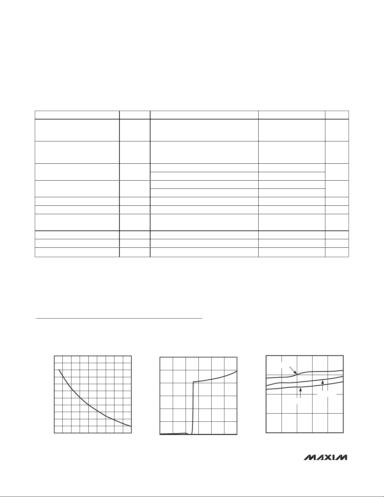
CURRENT-LIMIT PROGRAM vs. R
1.6
1.5
1.4
1.3
1.2
1.1
1.0
0.9
CURRENT LIMIT (A)
0.8
0.7
0.6
0.5
24 60
R
40 48 52 564428 3632
ISET
(kΩ)
ISET
MAX1558/58H toc01
QUIESCENT CURRENT (μA)
QUIESCENT SUPPLY CURRENT
vs. SUPPLY VOLTAGE
60
50
40
30
20
10
0
06
SUPPLY VOLTAGE (V)
54321
QUIESCENT CURRENT vs. TEMPERATURE
50
V
= 5.5V
IN_
45
MAX1558/58H toc02
40
V
IN_
QUIESCENT CURRENT (μA)
35
30
-40 85
TEMPERATURE (°C)
V
= 4.5V
= 5V
IN_
603510-15
MAX1558/58H toc03
Page 5
MAX1558/MAX1558H
Dual, 3mm x 3mm, 1.2A/Programmable-Current
USB Switches with Autoreset
_______________________________________________________________________________________
5
Typical Operating Characteristics (continued)
(V
INA
= V
INB
= 5V, V
ONA
= V
ONB
= 0V (MAX1558), V
ONA
= V
ONB
= 5V (MAX1558H), R
ISET
= 26kΩ to GND. Typical values are at TA=
+25°C, unless otherwise noted.)
SHUTDOWN CURRENT vs. TEMPERATURE
4.0
ON_ = V
(MAX1558)
IN_
ON_ = GND (MAX1558H)
3.5
3.0
2.5
2.0
1.5
SHUTDOWN CURRENT (μA)
1.0
0.5
0
-40 85
TEMPERATURE (°C)
NORMALIZED ON-RESISTANCE
vs. TEMPERATURE
1.50
1.25
(Ω)
ON
1.00
NORMALIZED R
0.75
0.50
-40 85
TEMPERATURE (°C)
1000
MAX1558/58H toc04
SWITCH OFF-LEAKAGE CURRENT (nA)
6035-15 10
603510-15
0.01
1.45
1.44
1.43
MAX1558/58H toc07
1.42
1.41
1.40
1.39
1.38
1.37
1.36
CONTINUOUS CURRENT-LIMIT THRESHOLD (A)
1.35
SWITCH OFF-LEAKAGE CURRENT
vs. TEMPERATURE
ON_ = IN_ (MAX1558)
ON_ = GND
(MAX1558H)
100
10
1
0.1
-40 85
TEMPERATURE (°C)
6035-15 10
CONTINUOUS CURRENT-LIMIT THRESHOLD
vs. TEMPERATURE
-40 85
TEMPERATURE (°C)
603510-15
OFF REVERSE-BLOCKING LEAKAGE
CURRENT vs. OUTPUT VOLTAGE
100
MAX1558/58H toc05
10
1
OFF REVERSE-BLOCKING LEAKAGE CURRRENT (nA)
0.1
06
OUTPUT VOLTAGE (V)
TURN-ON TIME
MAX1558/58H toc08
TURN-ON TIME (ms)
vs. TEMPERATURE (t
8
7
V
= 4.5V
IN_
6
5
V
= 5V
IN_
4
3
-40 85
TEMPERATURE (°C)
ON
V
= 5.5V
IN_
+ t
RISE
603510-15
MAX1558/58H toc06
54321
)
MAX1558/58H toc09
TURN-OFF TIME
vs. TEMPERATURE (t
4.00
3.75
3.50
3.25
3.00
2.75
TURN-OFF TIME (ms)
2.50
2.25
2.00
-40 85
V
IN_
V
= 4.5V
IN_
= 5.5V
TEMPERATURE (°C)
OFF
V
= 5V
IN_
+ t
FALL
603510-15
)
25
MAX1558/58H toc10
24
23
22
FAULT-BLANKING TIME (ms)
21
20
FAULT-BLANKING TIME
vs. TEMPERATURE
V
= 4.5V
IN_
V
= 5V
IN_
V
= 5.5V
IN_
-40 80
TEMPERATURE (°C)
655035205-10-25
FAULT OUTPUT LOW VOLTAGE
275
250
MAX1558/58H toc11
225
200
175
150
FAULT OUTPUT LOW VOLTAGE (mV)
125
100
V
IN_
-40 85
vs. TEMPERATURE
= 4.5V
V
= 5.5V
IN_
TEMPERATURE (°C)
MAX1558/58H toc12
V
= 5V
IN_
603510-15
Page 6

MAX1558/MAX1558H
Dual, 3mm x 3mm, 1.2A/Programmable-Current
USB Switches with Autoreset
6 _______________________________________________________________________________________
Typical Operating Characteristics (continued)
(V
INA
= V
INB
= 5V, V
ONA
= V
ONB
= 0V (MAX1558), V
ONA
= V
ONB
= 5V (MAX1558H), R
ISET
= 26kΩ to GND. Typical values are at TA=
+25°C, unless otherwise noted.)
AUTORESET CURRENT
vs. TEMPERATURE
40
38
36
34
32
30
28
26
AUTORESET CURRENT (mA)
24
22
20
-40 85
OVERLOAD RESPONSE INTO 2.5Ω
V
IN
OUT_
FLT_
I
OUT_
V
= 5.5V
IN_
V
= 4.5V
IN_
TEMPERATURE (°C)
V
= 5V
IN_
MAX1558/58H toc15
603510-15
MAX1558/58H toc13
5V
5V/div
0
5V/div
0
1A/div
0
AUTORESET CURRENT
vs. INPUT VOLTAGE
40
35
30
AUTORESET CURRENT (mA)
25
20
3.0 6.0
TA = -40°C
TA = +85°C
TA = +25°C
VIN (V)
SHORT-CIRCUIT RESPONSE INTO 0Ω
V
IN
V
OUT
FLTA_
I
OUT_
SHORT
APPLIED
SHORT
REMOVED
AUTORESTART
5.55.04.54.03.5
MAX1558/58H toc16
SWITCH ON
MAX1558/58H toc14
5V/div
0
5V/div
0
5V/div
0
5A/div
0
ON_
OUT_
20ms/div
SWITCH TURN-ON TIME
2.0ms/div
MAX1558/58H toc17
2V/div
0
2V/div
0
ON_
OUT_
20ms/div
SWITCH TURN-OFF TIME
1.0ms/div
MAX1558/58H toc18
2V/div
0
2V/div
0
Page 7

Detailed Description
The MAX1558/MAX1558H are dual current-limited
switches designed for USB applications. They have two
independent switches, each with its own enable control
input and autoreset function. Each switch has an errorflag output to notify the USB controller when currentlimit, short-circuit, undervoltage-lockout, or thermalshutdown conditions occur (Figure 2). The MAX1558/
MAX1558H operate from a 2.7V to 5.5V supply. Each
output can supply up to 1.2A. Current limit for both
channels is set with one external resistor.
The MAX1558/MAX1558H have independent thermal
shutdown for each switch in the event of a prolonged
overload. An autoreset function monitors the output and
automatically turns the switch on when the overload is
removed. Separate current limiting and thermal-shutdown circuits permit each switch to operate independently, improving system robustness.
MAX1558/MAX1558H
Pin Description
Dual, 3mm x 3mm, 1.2A/Programmable-Current
USB Switches with Autoreset
_______________________________________________________________________________________ 7
*
( ) are for the MAX1558H only.
Figure 1. Typical Application Circuit
PIN NAME FUNCTION
1 INA
2
3 ISET
4
5 INB
6 OUTB
7 FLTB
8 GND
9 FLTA
10 OUTA
— PAD
ONA
*(ONA)
ONB
*(ONB)
Power Input for OUTA. Connect INA and INB together and bypass with a 0.1µF capacitor to ground.
Load conditions may require additional bulk capacitance to prevent the input from being pulled down.
Control Input for Switch A. Can be driven higher than IN_ without damage. A logic low turns switch A on
for the MAX1558. A logic high turns switch A on for the MAX1558H.
Current-Limit Adjust for Both Channels. Connect a resistor between 26kΩ to 60kΩ from ISET to ground to
program the current limit. See Setting the Current Limit in the Applications Information section.
Control Input for Switch B. Can be driven higher than IN_ without damage. A logic low turns switch B on
for the MAX1558. A logic high turns switch B on for the MAX1558H.
Power Input for OUTB. Connect INB and INA together and bypass with a 0.1µF capacitor to ground.
Load conditions may require additional bulk capacitance to prevent the input from being pulled down.
Power Output for Switch B. Connect a 1µF capacitor from OUTB to ground. The load condition may
require additional bulk capacitance.
Fault Indicator Output for Switch B. This open-drain output goes low when switch B is in thermal
shutdown or UVLO or in a sustained (>20ms) current-limit or short-circuit condition.
Ground
Fault Indicator Output for Switch A. This open-drain output goes low when switch A is in thermal
shutdown or UVLO or in a sustained (>20ms) current-limit or short-circuit condition.
Power Output for Switch A. Connect a 1µF capacitor from OUTA to ground. The load condition may
require additional bulk capacitance.
Exposed Pad, Internally Connected to GND. Connect exposed pad to a large copper trace for maximum
power dissipation.
0.1μF
INA
INPUT
2.7V TO 5.5V
100kΩ
INB
100kΩ
MAX1558
FLTA
FLTB
ISET
*USB APPLICATIONS MAY REQUIRE ADDITIONAL
BULK CAPACITANCE
ONA
ONB
OUTA
OUTB
GND
ONA
ONB
1μF*
1μF*
USB
PORT A
USB
PORT B
Page 8

MAX1558/MAX1558H
Dual, 3mm x 3mm, 1.2A/Programmable-Current
USB Switches with Autoreset
8 _______________________________________________________________________________________
Figure 2. Functional Diagram
INA
FLTA
INA
ONA
ONA
ONB
ONB
INB
0.6V
CHARGE
PUMP
BIAS
UVLO
REF
OSC
25kHz
CHARGE
PUMP
THERMAL
SHUTDOWN
TIMER
20ms
ILIMA
30mA
FAULT
LOGIC
30mA
ILIMB
PROGRAM ILIMA
PROGRAM ILIMB
OUTA
GND
OUTB
INB
FLTB
MAX1558
ISET
Page 9

MAX1558/MAX1558H
Dual, 3mm x 3mm, 1.2A/Programmable-Current
USB Switches with Autoreset
_______________________________________________________________________________________ 9
Undervoltage Lockout and
Input Voltage Requirements
The MAX1558/MAX1558H include a UVLO circuit to
prevent erroneous switch operation when the input voltage is low during startup and brownout conditions.
Operation is inhibited when V
IN_
is less than 2.5V.
Output-Current Fault Protection
The current limit for both switch outputs is programmed
by a resistor between 26kΩ and 60kΩ connected from
ISET to ground. See the Current-Limit Program vs. R
ISET
curve in the
Typical Operating Characteristics
and
Setting
the Current Limit
in the
Applications Information
section.
The MAX1558 reduces the gate drive to the MOSFET
switch when the programmed current-limit value is
reached. If the current-limit program value is reached, the
part reduces gate drive to regulate at the current limit. If
the current limit persists for 20ms (typ), the output turns
off and the fault flag is set until the fault is removed, as
detected by the autoreset circuit.
When the the output drops below 1V (typ), the current
limit is set 30% above the programmed level and
pulsed. This lowers the RMS current for a short-circuit
condition, which reduces system load current and
power dissipation. If a short circuit persists for 20ms,
the output turns off and the fault flag is set. The autoreset circuit automatically restarts the part if the fault is
removed.
Fault Blanking
The MAX1558/MAX1558H switches can reach current
limit in normal operation when powering up or driving
heavy capacitive loads. To differentiate these conditions
from short circuits or sustained overloads, the
MAX1558/MAX1558H have independent fault-blanking
circuits in each switch. When a load transient causes
the device to enter the current limit, an internal counter
monitors the duration of the fault. For load faults exceeding the 20ms fault-blanking time, the offending switch
turns off, the corresponding FLT_ signal asserts low,
and that channel enters autoreset mode (see the
Autoreset Mode
section). Only current-limit and shortcircuit faults are blanked. Thermal-overload faults and
input-voltage drops below the UVLO threshold immediately cause the switch to turn off and FLT_ to assert low.
Fault blanking allows the MAX1558 to handle USB
loads that may not be fully compliant with USB specifications. USB loads with additional bypass capacitance
and/or large startup currents can be successfully powered even while protecting the upstream power source.
No fault is indicated if the switch is able to bring up the
load within the 20ms blanking period.
Autoreset Mode
If an output fault is detected for more than the 20ms
blanking time, the output latches off and the FLT_ out-
put goes low. The MAX1558/MAX1558H then source
30mA to the faulted output and monitor the output voltage to determine when the overload is removed. If the
voltage on the output rises above 0.5V for more than
20ms, the fault resets and the output turns on. The
MAX1558 can also be reset from fault manually by toggling ON_ (ON_ for the MAX1558H) for that channel.
Reverse Current Blocking
The USB specification does not allow an output device
to source current back into the USB port. However, the
MAX1558/MAX1558H are designed to safely power
noncompliant devices. When disabled, each output is
switched to a high-impedance state, blocking reversecurrent flow from the output back to the input. However,
during normal operation with the device enabled, the
MAX1558/MAX1558H are bidirectional switches.
Thermal Shutdown
The MAX1558/MAX1558H feature independent thermal
shutdown for each switch channel, allowing one switch
to deliver power even if the other switch has a fault condition. When the junction temperature exceeds +160°C,
the switch turns off and the FLT_ output goes low immediately; fault blanking does not occur during thermal
limit. When the junction cools by 10°C, the switch turns
on again. If the fault-overload condition continues, the
switch cycles on and off, resulting in a pulsed output,
saving battery power.
Fault Indicators
The MAX1558/MAX1558H provide an open-drain fault
output (FLT_) for each switch. For most applications, connect FLT_ to IN_ through a 100kΩ pullup resistor. FLT_
goes low when any of the following conditions occur:
• The input voltage is below the UVLO threshold.
• The switch junction temperature exceeds the +160°C
thermal-shutdown temperature limit.
• The switch is in current-limit or short-circuit limit mode
after the 20ms fault-blanking period is exceeded.
• The switch is in autoreset mode.
After the fault condition is removed, the FLT_ output
deasserts after a 20ms delay. Ensure that the
MAX1558/MAX1558H have adequate input bypass
capacitance to prevent glitches from triggering FLT_ out-
puts. Glitches that cause the input supply to drop below
2.5V may cause the undervoltage lockout to trigger, turn-
ing the outputs off and asserting the FLT signals.
Page 10

MAX1558/MAX1558H
Dual, 3mm x 3mm, 1.2A/Programmable-Current
USB Switches with Autoreset
10 ______________________________________________________________________________________
Applications Information
Setting the Current Limit
A resistor from ISET to ground programs the currentlimit value for both outputs. Use a resistor between
26kΩ and 86kΩ to set the current limit according to
the formula:
I
LIM(TYPICAL)
= 36400 / R
ISET
(Amps)
Do not use R
ISET
values below 26kΩ because the maximum current rating of the device may be exceeded.
R
ISET
values larger than 60kΩ are not recommended
and do not provide a lower limit current than 500mA.
If the output drops below 1V (typ), the MAX1558 shifts
to a short-circuit current-limit threshold that is 30%
above the programmed level given by the I
LIM(TYPICAL)
formula. If the short-circuit threshold is exceeded, the
switch shuts off immediately (no 20ms delay) and
ramps the current back up in approximately 3ms. If the
short persists and the current ramps all the way up to
the short-circuit limit again, the switch again turns off. If
the short still persists, the output pulses this way for
20ms, at which time the switch turns off and autoreset
mode begins.
Input Capacitor
INA and INB provide the power for all control and
charge-pump circuitry and must be connected together
externally. Connect a capacitor from IN_ to ground to
limit the input-voltage drop during momentary output
short-circuit conditions. A 0.1µF ceramic capacitor is
required for local decoupling; higher capacitor values
further reduce the voltage drop at the input. When driving inductive loads, a larger capacitance prevents
voltage spikes from exceeding the MAX1558/
MAX1558Hs’ absolute maximum ratings.
Output Capacitor
Place a 1µF or greater capacitor at each output for
noise immunity. When starting up into very large capacitive loads, the switch may pulse the output current at
the short-circuit current-limit program level until the output voltage rises above 1V. Then, the capacitor continues to charge at the full, continuous current-limit
program level. There is no limit to the output capacitor
size, but to prevent a startup fault assertion, the capacitor must charge up within the fault-blanking delay period. Typically, starting up into a 500µF or smaller
capacitor does not trigger a fault output. In addition to
bulk capacitance, small-value (0.1µF or greater) ceramic capacitors improve the output’s resilience to electrostatic discharge (ESD).
Driving Inductive Loads
A wide variety of devices (mice, keyboards, cameras,
and printers) can load the USB port. These devices commonly connect to the port with cables, which can add an
inductive component to the load. This inductance causes the output voltage at the USB port to ring during a
load step. The MAX1558/MAX1558H are capable of driving inductive loads, but avoid exceeding the devices’
absolute maximum ratings. Usually the load inductance
is relatively small, and the MAX1558/MAX1558Hs’
input includes a substantial bulk capacitance from an
upstream regulator as well as local bypass capacitors,
limiting overshoot. If severe ringing occurs due to large
load inductance, clamp the MAX1558/MAX1558Hs’ output below +6V and above -0.3V.
Turn-On and Turn-Off Behavior
In the absence of faults, the MAX1558/MAX1558Hs’
internal switches turn on and off slowly under the control
of the ON_ inputs. Transition times for both edges are
approximately 4ms. The slow charge-pump switch drive
minimizes load transients on the upstream power source.
Under thermal fault and UVLO, the power device turns
off rapidly (100ns) to protect the power device.
Layout and Thermal Dissipation
To optimize the switch response time to output shortcircuit conditions, keep all traces as short as possible
to reduce the effect of undesirable parasitic inductance. Place input and output capacitors no more than
5mm from device leads. All IN_ and OUT_ pins must be
connected with short traces to the power bus. Wide
power-bus planes provide superior heat dissipation
through the switch IN_ and OUT_ pins. While the
switches are on, power dissipation is small and the
package temperature change is minimal. Calculate the
power dissipation for this condition as follows:
P = (I
OUT
_)2R
ON
For the maximum operating current (I
OUT
_ = 1.2A) and
the maximum on-resistance of the switch (125mΩ), the
power dissipation is:
P = (1.2A)2x 0.125Ω = 180mW per switch
The worst-case power dissipation occurs when the
switch is in current limit and the output is greater than
1V. The instantaneous power dissipated in each switch
is the voltage drop across the switch multiplied by the
current limit. The fault-blanking circuit turns the output
off if the fault persists for 20ms, while the autoreset circuit can turn it back on after 20ms in the off state. Thus,
the average worst-case power is approximately 50% of
the instantaneous value.
P = 0.5 x (I
LIM
) x (V
IN_
- V
OUT_
)
Page 11

For a 5V input and 1V output, the maximum possible
power dissipation per switch is:
P = 0.5 x (1.5A) x (5V - 1V) = 3W
Since the package power dissipation is limited to
1952mW, the MAX1558/MAX1558H die temperature
exceeds the thermal-shutdown threshold and the
switch turns off. After the die temperature cools by
10°C, the switch turns on again. If the fault-overload
condition continues, the switch cycles on and off with a
duty cycle and period that is a function of the ambient
temperature and PC board layout.
A short across the output for more than 20ms places
the part in autoreset mode. With V
IN_
= 5V and an
autoreset test current of 30mA, the power dissipation
for a short-circuited output is given by:
P = (30mA) x 5V = 0.15W
MAX1558/MAX1558H
Dual, 3mm x 3mm, 1.2A/Programmable-Current
USB Switches with Autoreset
______________________________________________________________________________________ 11
Chip Information
TRANSISTOR COUNT: 2932
PROCESS: BiCMOS
Page 12

MAX1558/MAX1558H
Dual, 3mm x 3mm, 1.2A/Programmable-Current
USB Switches with Autoreset
12 ______________________________________________________________________________________
Package Information
(The package drawing(s) in this data sheet may not reflect the most current specifications. For the latest package outline information,
go to www.maxim-ic.com/packages
.)
6, 8, &10L, DFN THIN.EPS
Page 13

MAX1558/MAX1558H
Dual, 3mm x 3mm, 1.2A/Programmable-Current
USB Switches with Autoreset
______________________________________________________________________________________ 13
Package Information (continued)
(The package drawing(s) in this data sheet may not reflect the most current specifications. For the latest package outline information,
go to www.maxim-ic.com/packages
.)
COMMON DIMENSIONS
SYMBOL MIN. MAX.
A 0.70 0.80
D 2.90 3.10
E 2.90 3.10
0.00 0.05
A1
L 0.20 0.40
0.25 MIN.k
A2 0.20 REF.
PACKAGE VARIATIONS
PKG. CODE N D2 E2 e JEDEC SPEC b
T633-2 6 1.50±0.10 2.30±0.10 0.95 BSC MO229 / WEEA 0.40±0.05 1.90 REF
T833-2 8 1.50±0.10 2.30±0.10 0.65 BSC MO229 / WEEC 0.30±0.05 1.95 REF
T833-3 8 1.50±0.10 2.30±0.10 0.65 BSC MO229 / WEEC 0.30±0.05 1.95 REF
1.50±0.10 MO229 / WEED-3
2.30±0.10 MO229 / WEED-3 2.00 REF0.25±0.050.50 BSC1.50±0.1010T1033-2
0.40 BSC - - - - 0.20±0.05 2.40 REFT1433-2 14 2.30±0.101.70±0.10
[(N/2)-1] x e
2.00 REF0.25±0.050.50 BSC2.30±0.1010T1033-1
2.40 REF0.20±0.05- - - - 0.40 BSC1.70±0.10 2.30±0.1014T1433-1
Page 14

MAX1558/MAX1558H
Dual, 3mm x 3mm, 1.2A/Programmable-Current
USB Switches with Autoreset
Maxim cannot assume responsibility for use of any circuitry other than circuitry entirely embodied in a Maxim product. No circuit patent licenses are
implied. Maxim reserves the right to change the circuitry and specifications without notice at any time.
14
____________________Maxim Integrated Products, 120 San Gabriel Drive, Sunnyvale, CA 94086 408-737-7600
© 2008 Maxim Integrated Products is a registered trademark of Maxim Integrated Products, Inc.
Revision History
REVISION
NUMBER
2 3/08 Changed “UL Listing Pending” to “UL Recognized: UL # E211395” 1
REVISION
DATE
DESCRIPTION
PAGES
CHANGED
 Loading...