

General Description
The MAX1512 is a programmable VCOM-adjustment
solution for thin-film transistor (TFT) liquid-crystal displays
(LCDs). The MAX1512 simplifies the labor-intensive
VCOM-adjustment process and replaces mechanical
potentiometers, which significantly reduces labor costs,
increases reliability, and enables automation.
The MAX1512 attaches to an external resistive voltagedivider and sinks a programmable current to set the
VCOM voltage level. An internal 7-bit digital-to-analog
converter (DAC) controls the sink current. The DAC is
ratiometric relative to AVDD and is guaranteed to be
monotonic over all operating conditions. This VCOM
calibrator IC includes an EEPROM to store the desired
VCOM voltage level. The EEPROM can be programmed
repeatedly, giving TFT LCD manufacturers the flexibility
to calibrate the display panel as many times as the
manufacturing process requires.
The IC features a single-wire interface between the
LCD panel and the programming circuit. The singlewire interface delivers both programming power and
DAC-adjustment commands to minimize changes to
panel connectors and production equipment. The
MAX1512 is available in an 8-pin 3mm x 3mm TDFN
package. A complete evaluation kit is available to simplify evaluation and production development.
Applications
LCD Panels
Notebook Computers
Monitors
LCD TVs
Features
♦ 7-Bit Adjustable Sink-Current Output
♦ Resistor-Adjustable Full-Scale Range
♦ Guaranteed Monotonic Output Over Operating
Range
♦ Single-Wire Adjustment and Programming*
♦ EEPROM Stores VCOM Setting
♦ Interface Enable/Disable Control (CE)
♦ 2.6V to 3.6V Logic Supply-Voltage Operating
Range (V
DD
)
♦ 4.5V to 20V Analog Supply-Voltage Range (V
AVDD
)
♦ V
DD
UVLO Protection
♦ 8-Pin 3mm x 3mm TDFN (0.8mm max)
MAX1512
EEPROM-Programmable TFT VCOM Calibrator
________________________________________________________________ Maxim Integrated Products 1
CE
CTL
AVDD
R
SET
OUT
R2
R1
VCOM
SET
GND
V
DD
V
DD
AVDD
MAX1512
Pin Configuration
Ordering Information
1
2
3
4
8
7
6
5
SET
CE
CTL
V
DD
GND
N.C.
AVDD
OUT
MAX1512
TDFN
TOP VIEW
Typical Operating Circuit
19-2911 Rev 2; 8/04
For pricing, delivery, and ordering information, please contact Maxim/Dallas Direct! at
1-888-629-4642, or visit Maxim’s website at www.maxim-ic.com.
PART
PIN-PACKAGE
MAX1512ETA
8 TDFN 3mm x 3mm
EVALUATION KIT
AVAILABLE
*Patent Pending.
查询MAX1512供应商
TEMP RANGE
-40°C to +85°C
MAX1512
EEPROM-Programmable TFT VCOM Calibrator
2 _______________________________________________________________________________________
ABSOLUTE MAXIMUM RATINGS
ELECTRICAL CHARACTERISTICS
(Circuit of Figure 1, VDD= 3V, V
AVDD
= 10V, V
OUT
= 5V, R
SET
= 30.1kΩ, TA= 0°C to +85°C, unless otherwise noted. Typical values
are at T
A
= +25°C.) (Note 1)
Stresses beyond those listed under “Absolute Maximum Ratings” may cause permanent damage to the device. These are stress ratings only, and functional
operation of the device at these or any other conditions beyond those indicated in the operational sections of the specifications is not implied. Exposure to
absolute maximum rating conditions for extended periods may affect device reliability.
VDD, SET, CE to GND...............................................-0.3V to +4V
OUT to GND ...........................................................-0.3V to +14V
AVDD to GND.........................................................-0.3V to +24V
CTL to GND ............................................................-0.3V to +16V
Continuous Power Dissipation (T
A
= +70°C) ...............................
8-Pin Thin QFN 3mm x 3mm (derate 24.4mW/°C
above +70°C).............................................................1951mW
Operating Temperature Range ...........................-40°C to +85°C
Junction Temperature......................................................+150°C
Storage Temperature Range .............................-65°C to +160°C
Lead Temperature (soldering, 10s) .................................+300°C
PARAMETER
SYMBOL
CONDITIONS
MIN
TYP
MAX
UNITS
SINK-CURRENT ADJUSTMENT
SET Voltage Resolution 7 Bits
SET Differential Nonlinearity Guaranteed monotonic -1 +1 LSB
SET Zero-Scale Error -1 +1 +2 LSB
SET Full-Scale Error -12
LSB
SET Current I
SET
120 µA
To GND, V
AVDD
= 20V 10 200
SET External Resistance (Note 2)
R
SET
To GND, V
AVDD
= 4.5V
kΩ
V
SET
/ V
AVDD
Voltage Ratio DAC full scale
V/V
V
SET
/ V
AVDD
Factory Set Voltage
Ratio
V/V
VDD SUPPLY
VDD Supply Range V
DD
2.6 3.6 V
CE = V
DD
32 55
VDD Supply Current I
DD
CE = GND 12 20
µA
Rising edge 2.2 2.5 2.7
VDD Power-On Reset Threshold
Falling edge 2.1 2.4 2.6
V
VDD Power-On Reset Hysteresis
mV
CONTROL AND PROGRAMMING
CE Input Low Voltage 2.6V < VDD < 3.6V 0.4 V
CE Input High Voltage 2.6V < VDD < 3.6V 1.6 V
CE Startup Time (Note 3) 1 ms
CTL High Voltage 2.6V < VDD < 3.6V
V
CTL Float Voltage 2.6V < VDD < 3.6V
V
CTL Low Voltage 2.6V < VDD < 3.6V
V
CTL Rejected Pulse Width 20 µs
CTL Minimum Pulse Width
µs
CTL Minimum Time Between
Pulses
10 µs
CTL = GND -10
CTL Input Current
CTL = V
DD
10
µA
+12
2.25 45.00
0.05
0.024 0.025 0.026
100
0.70 x V
0.40 x V
0.20 x V
DD
DD
DD
0.82 x V
0.62 x V
0.32 x V
DD
DD
DD
200
MAX1512
EEPROM-Programmable TFT VCOM Calibrator
_______________________________________________________________________________________ 3
ELECTRICAL CHARACTERISTICS
(VDD= 3V, V
AVDD
= 10V, V
OUT
= 5V, R
SET
= 30.1kΩ, TA= -40°C to +85°C, unless otherwise noted.) (Note 1)
Note 1: Limits are 100% production tested at T
A
= +25°C. Limits over the operating temperature range are guaranteed through
correlation using standard quality control (SQC) methods.
Note 2: SET external resistor range is verified at DAC full scale.
Note 3: Guaranteed by design. Not production tested.
ELECTRICAL CHARACTERISTICS (continued)
(Circuit of Figure 1, VDD= 3V, V
AVDD
= 10V, V
OUT
= 5V, R
SET
= 30.1kΩ, TA= 0°C to +85°C, unless otherwise noted. Typical values
are at T
A
= +25°C.) (Note 1)
CTL Input Current
CTL = V
DD
10
µA
PARAMETER
CONDITIONS
UNITS
CTL EEPROM Program Voltage V
PP
(Note 3)
V
OUTPUT VOLTAGE
OUT Leakage Current V
DD
= 2.1V 1 nA
OUT Settling Time To ±0.5 LSB error band 20 µs
V
OUT
Voltage Range V
OUT
13 V
AVDD SUPPLY
V
AVDD
Supply Range V
AVDD
4.5
V
SYMBOL
MIN TYP MAX
15.25 15.5 15.75
V
+ 0.5V
SET
SINK-CURRENT ADJUSTMENT
SET Differential Nonlinearity Guaranteed monotonic -1 +1 LSB
SET Zero-Scale Error -1 +2 LSB
SET Full-Scale Error -12 +12 LSB
SET Current I
SET External Resistance (Note 2) R
VDD SUPPLY
VDD Supply Range V
VDD Supply Current I
VDD Power-On Reset Threshold
CONTROL AND PROGRAMMING
CE Input Low Voltage 2.6V < VDD < 3.6V 0.4 V
CE Input High Voltage 2.6V < VDD < 3.6V 1.6 V
AVDD SUPPLY
V
AVDD
AVDD Operating Current I
PARAMETER SYMBOL CONDITIONS MIN TYP MAX UNITS
SET
SET
DD
DD
To GND, V
To GND, V
= 20V 10 200
AVDD
= 4.5V 2.25 45.00
AVDD
2.6 3.6 V
CE = V
DD
CE = GND 20
120 µA
55
Rising edge 2.2 2.7
Falling edge 2.1 2.6
Supply Range V
AVDD
AVDD
V
= 20V 20 µA
AVDD
4.5 20.0 V
20.0
kΩ
µA
V
MAX1512
EEPROM-Programmable TFT VCOM Calibrator
4 _______________________________________________________________________________________
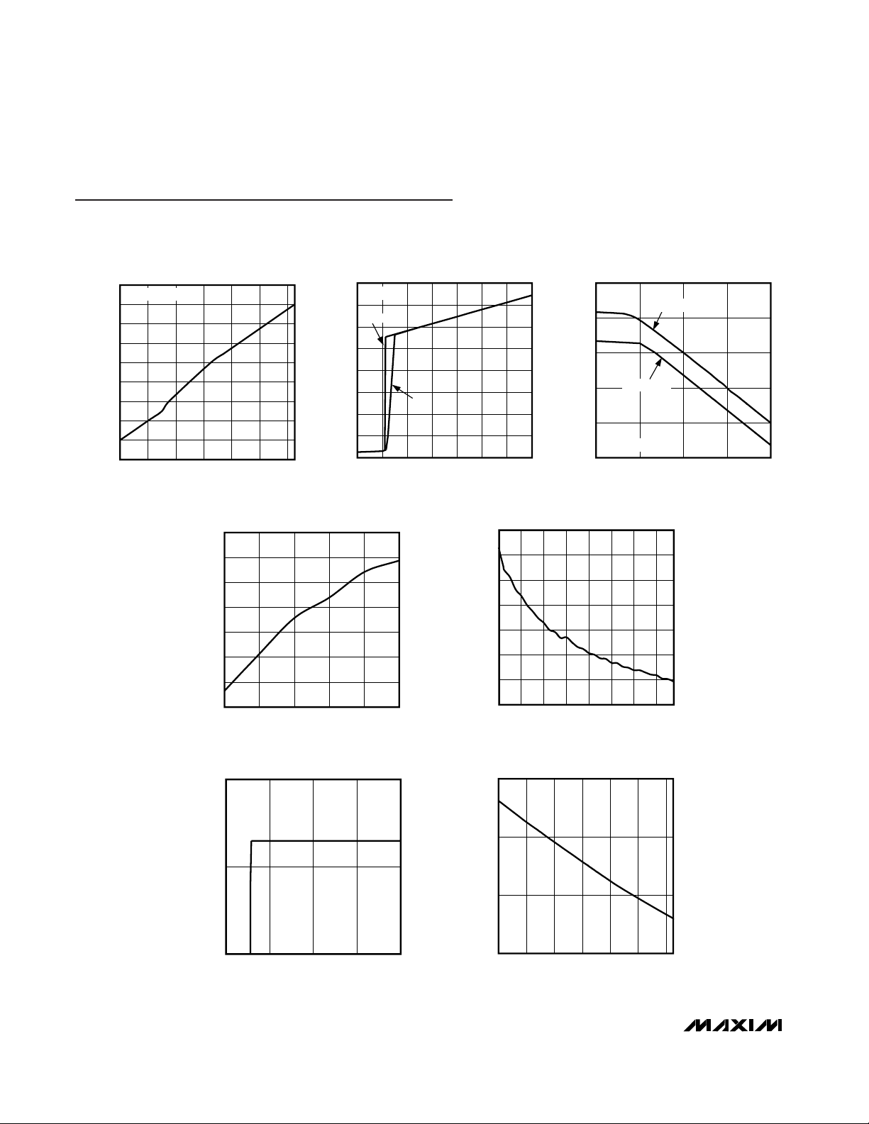
Typical Operating Characteristics
(Circuit of Figure 1, VDD= 3V, V
AVDD
= 10V, V
OUT
= 5V, R
SET
= 24.9kΩ, TA= +25°C, DAC half scale, unless otherwise noted.)
VDD SUPPLY CURRENT
vs. TEMPERATURE
MAX1512 toc01
TEMPERATURE (°C)
V
DD
SUPPLY CURRENT (µA)
806020 400-20
31.6
31.8
32.0
32.2
32.4
32.6
32.8
33.0
33.2
31.4
-40
CE = VDD = 3V
VDD SUPPLY CURRENT vs. V
DD
MAX1512 toc02
VDD (V)
V
DD
SUPPLY CURRENT (µA)
3.43.22.4 2.6 2.8 3.0
5
10
15
20
25
30
35
40
0
2.2 3.6
RISING
FALLING
CE = V
DD
I
OUT
vs. R
SET
MAX1512 toc03
R
SET
(kΩ)
I
OUT
(µA)
100101
1
10
100
1000
10,000
0.1
0.1 1000
V
AVDD
= 20V
V
AVDD
= 4.5V
VDD = V
OUT
= 3V
I
OUT
SINK-CURRENT ERROR vs. V
DD
MAX1512 toc04
VDD (V)
I
OUT
SINK-CURRENT ERROR (LSB)
3.43.23.02.8
2.825
2.830
2.835
2.840
2.845
2.850
2.855
2.820
2.6 3.6
I
OUT
SINK-CURRENT ERROR vs. V
AVDD
MAX1512 toc05
V
AVDD
(V)
I
OUT
SINK-CURRENT ERROR (LSB)
18.516.514.512.510.58.56.5
2.75
2.80
2.85
2.90
2.95
3.00
3.05
2.70
4.5
I
OUT
SINK-CURRENT ERROR vs. V
OUT
MAX1512 toc06
V
OUT
(V)
I
OUT
SINK-CURRENT ERROR (LSB)
1.51.00.5
2.835
0 2.0
2.840
2.830
I
OUT
SINK-CURRENT ERROR
vs. TEMPERATURE
MAX1512 toc07
TEMPERATURE (°C)
I
OUT
SINK-CURRENT ERROR (LSB)
806040200-20
2.8
2.9
3.0
2.7
-40

MAX1512
EEPROM-Programmable TFT VCOM Calibrator
_______________________________________________________________________________________ 5
Typical Operating Characteristics (continued)
(Circuit of Figure 1, VDD= 3V, V
AVDD
= 10V, V
OUT
= 5V, R
SET
= 24.9kΩ, TA= +25°C, DAC half scale, unless otherwise noted.)
TOTAL UNADJUSTED ERROR
vs. DAC SETTING
MAX1512 toc08
DAC SETTING
TOTAL UNADJUSTED ERROR (LSB)
112968064483216
1
2
3
4
5
6
7
0
0128
R
SET
= 25kΩ
R
SET
= 100kΩ
INTEGRAL NONLINEARITY
vs. DAC SETTING
MAX1512 toc09
DAC SETTING
INTEGRAL NON-LINEARITY (LSB)
1129664 8032 4816
-0.8
-0.6
-0.4
-0.2
0
0.2
0.4
0.6
0.8
1.0
-1.0
0128
R
SET
= 100kΩ
R
SET
= 25kΩ
DIFFERENTIAL NONLINEARITY
vs. DAC SETTING
MAX1512 toc10
DAC SETTING
DIFFERENTIAL NON-LINEARITY (LSB)
1129664 8032 4816
-0.8
-0.6
-0.4
-0.2
0
0.2
0.4
0.6
0.8
1.0
-1.0
0128
AVDD POWER-UP RESPONSE
MAX1512 toc11
0
0
V
AVDD
10V/div
40µs/div
V
OUT
1V/div
0
V
DD
2V/div
C
OUT
= 100pF
VDD POWER-UP RESPONSE
MAX1512 toc12
0
4V
5V
40µs/div
10V
0
V
DD
2V/div
V
OUT
V
AVDD
C
OUT
= 100pF
SINGLE LSB STEP-UP RESPONSE
MAX1512 toc13
0
V
OUT
5mV/div
40µs/div
V
CTL
2V
C
OUT
= 100pF
SINGLE LSB STEP-DOWN RESPONSE
MAX1512 toc14
0
V
OUT
5mV/div
40µs/div
V
CTL
2V
C
OUT
= 100pF

MAX1512
EEPROM-Programmable TFT VCOM Calibrator
6 _______________________________________________________________________________________
Detailed Description
The MAX1512 is a solid-state alternative to mechanical
potentiometers used for adjusting the LCD backplane
voltage (VCOM) in TFT LCD displays. The MAX1512
attaches to an external resistive voltage-divider and
sinks a programmable current (I
OUT
), which sets the
VCOM level (Figure 1). An internal 7-bit DAC controls
the sink current and allows the user to increase or
decrease the VCOM level (Figure 2). The DAC is ratiometric relative to AVDD and is monotonic over all operating conditions. The user can store the DAC setting in
an internal EEPROM. On power-up, the EEPROM presets the DAC to the last stored setting. The single-wire
interface between the LCD panel and the programming
circuit adjusts the DAC, programs the EEPROM, and
provides programming power.
The resistive voltage-divider and the AVDD supply set
the maximum value of VCOM. The MAX1512 sinks current from the voltage-divider to reduce the VCOM level.
The external resistor R
SET
sets the full-scale sink cur-
rent and the minimum value of VCOM.
Pin Description
PIN
FUNCTION
1 OUT
Adjustable Sink-Current Output. OUT connects to the resistive voltage-divider between AVDD and GND that
sets the VCOM voltage. I
OUT
lowers the divider voltage by an adjustable amount. See the SET pin
description.
2 AVDD High-Voltage Analog Supply. Connects to the panel source-driver supply rail.
3N.C. No Connect. Not internally connected.
4 GND Ground
5VDDSupply Input. +2.6V to +3.6V input range.
6 CTL
VCOM Adjustment and EEPROM Programming Control. CTL sets the internal DAC code and programs the
EEPROM. A pulse-control method is used to adjust the VCOM level. See the VCOM Adjustment (CTL)
section. To program the DAC setting into the EEPROM as the power-on default, drive CTL to the EEPROM
programming voltage using the correct timing and voltage ramp rates. See the EEPROM Programming
(CTL) section.
7CE
Control Interface Enable. Connect CE to V
DD
to enable the CTL input. Connect CE to GND to disable the
CTL input and reduce the supply current.
8 SET
Full-Scale Sink-Current Adjustment Input. Connect a resistor, R
SET
, from SET to GND to set the full-scale
adjustable sink current. The full-scale adjustable sink current is equal to:
I
OUT
is equal to the current through R
SET
.
Figure 1. Standard Application Circuit
V
R
AVDD
SET
20 ×
NAME
V
DD
3V
AVDD
V
DD
CE
MAX1512
CTL
AVDD
OUT
SET
GND
10V
R
SET
25kΩ
R1
200kΩ
R2
245kΩ
VCOM
5V

MAX1512
EEPROM-Programmable TFT VCOM Calibrator
_______________________________________________________________________________________ 7
Setting the VCOM
Adjustment Range (R
SET
)
The external resistive voltage-divider sets the maximum
value of the VCOM adjustment range. R
SET
sets the
full-scale sink current, I
OUT
, which determines the mini-
mum value of the VCOM adjustment range. Large R
SET
values increase resolution but decrease the VCOM
adjustment range. Calculate R1, R2, and R
SET
using
the following procedure:
1) Choose the maximum VCOM level (V
MAX
), the mini-
mum VCOM level (V
MIN
), and the AVDD supply
voltage (V
AVDD
).
2) Calculate the R1 / R2 ratio:
3) Calculate the R1 / R
SET
ratio:
4) Choose R
SET
according to the limits shown in the
Electrical Characteristics section and calculate the
values for R1 and R2.
5) The resulting resolution is:
A complete design example is given below:
1) V
MAX
= 5V, V
MIN
= 3V, V
AVDD
= 10V
4) If R
SET
= 24.9kΩ, then R1 = 200kΩ and R2 =
200kΩ
5) Resolution = 15.75mV
3
1
20
53
5
8)
R
R
SET
=×
()
=
-
2
1210
5
1)
R
R
≅ =-1
Re
solutionV=
()
MAX MIN
-V
127
R
R
V
V
SET MAX
1
20
≅
()
×
MAX MIN
-V
R
R
V
V
AVDD
MAX
1
2
1 ≅ -
CE
R
CTL
7
7
CTL
AVDD
R
SET
OUT
R2
R1
19R
DAC
EEPROM
VCOM
SET
GND
V
DD
V
DD
AVDD
MAX1512
CONTROL
INTERFACE
Figure 2. Simplified Functional Diagram

MAX1512
Translating Existing Potentiometer
Circuits
Existing VCOM adjustment circuits using conventional
mechanical potentiometers can be translated into
MAX1512 circuits. Figures 3 and 4 show two common
adjustment circuits and their equivalent MAX1512 circuits.
Interface Enable/Disable (CE)
The MAX1512 control interface can be disabled to
reduce the VDDsupply current. Connect CE to GND to
reduce the typical supply current from 32µA to 12µA.
Connect CE to VDDto enable the control interface.
EEPROM-Programmable TFT VCOM Calibrator
8 _______________________________________________________________________________________
AVDD
R
SET
R
SET
=
OUT
R2
R1
R1 = Ra
R2 = Rb + Rc
Ra × (Rb + Rc)
20 × Rb
VCOM
SET
AVDD
MAX1512
Rb
Ra
VCOM
AVDD
Rc
MECHANICAL
POTENTIOMETER
MAX1512
EQUIVALENT CIRCUIT
Figure 3. Replacement of Mechanical/Potentiometer Circuit
AVDD
R
SET
R
SET
=
OUT
R2
R1
R1 = Rd
R2 = Rf
Rd × (Rd + Re + Rf)
20 × Re
VCOM
SET
AVDD
MAX1512
Re
Rd
VCOM
AVDD
Rf
MECHANICAL
POTENTIOMETER
MAX1512
EQUIVALENT CIRCUIT
Figure 4. Replacement of Mechanical/Potentiometer Circuit

The programming circuit in Figure 5 drives CE high to
enable the CTL input when it is connected. When the
programming circuit is not connected, CE is pulled low
through resistor R
CE
, which disables the CTL input. The
CTL input is relatively immune to noise and brief voltage transients. It can be safely left continuously
enabled if higher supply current is acceptable.
VCOM Adjustment (CTL)
Pulse CTL low for more than 200µs to increment the DAC
setting, which increases the OUT sink current and lowers
the VCOM level by 1 least-significant bit (LSB) (Figure 6).
Similarly, pulse CTL high for more than 200µs to decrement the DAC setting, which decreases the OUT sink current and increases the VCOM level by 1 LSB.
MAX1512
EEPROM-Programmable TFT VCOM Calibrator
_______________________________________________________________________________________ 9
CE
CTL
GND
MAX1512
PROGRAMMING
CIRCUIT
R
CE
V
DD
Figure 5. Optional Circuit to Drive CE
>1ms >200µs >200µs >200µs >10µs <20µs <20µs>200µs
CTL HIGH
V
DD
/2
CTL LOW
CTL
DAC SETTING
CE / V
DD
VCOM
CTL
ENABLED
64 65 64 63
UNDEFINED
FIRST
COUNT
IGNORED
SHORT
COUNTS
IGNORED
VCOM UP
VCOM DOWN
Figure 6. VCOM Adjustment

MAX1512
To avoid unintentional VCOM adjustment, the MAX1512
is guaranteed to reject CTL pulses shorter than 20µs. In
addition, to avoid the possibility of a single false pulse
caused by power-up sequencing between V
DD
and
CTL, the very first pulse is ignored.
EEPROM Programming (CTL)
To program the EEPROM, apply the EEPROM programming waveform through the CTL interface (Figure 7).
The control interface delivers programming power and
DAC adjustment commands on the same wire. This
1-wire approach minimizes the number of connections
from the programming circuit to the LCD panel.
To apply the EEPROM programming waveform, carefully
ramp CTL from midscale (V
DD
/ 2) to the programming
voltage, V
PP
, in 7.5ms as shown in Figure 7. If the ramp
is generated digitally, use at least 45 steps to achieve
the required 320mV ramp resolution. During the ramp
time, VCOM adjustment is disabled and the EEPROM
cells are biased in preparation for programming. After
reaching VPP, hold CTL at VPPfor 1ms. During the
EFPROM program time, the EEPROM stores the DAC
setting. Next, drive CTL to ground in less than 1ms and
hold for at least 200µs. Finally, drive CTL to V
DD
/ 2 to
complete the write cycle. The EEPROM is factory set to
half scale. Follow the EEPROM Programming Spec-
ifications in Table 1 to guarantee reliable EEPROM programming. Violating the specifications can damage the
EEPROM or affect data retention.
A complete evaluation kit is available to simplify evaluation and production development.
EEPROM-Programmable TFT VCOM Calibrator
10 ______________________________________________________________________________________
Table 1. EEPROM Programming Specifications
PARAMETER SYMBOL MIN TYP MAX UNITS
CTL Programming Voltage V
PP
15.25 15.5 15.75 V
CTL Programming Ramp T1 7.0 7.5 8.0 ms
EEPROM Program Time T2 0.9 1.0 1.1 ms
VPP Fall Time T3 10 1000 µs
Done Hold Time T4 200 µs
Figure 7. EEPROM Programming
CTL VOLTAGE
V
PP
/ 2
V
DD
0
T1
T2 T4T3
TIME

Applications Information
The VCOM adjustment and the EEPROM programming
must be performed with an external programming circuit. Refer to the MAX1512 evaluation kit for a complete
programming circuit solution.
Use a circuit similar to the conceptual diagram shown
in Figure 8 to drive CTL. The accuracy of the programming voltage (V
PP
) is critical for proper MAX1512 data
retention. The use of a comparator is recommended to
verify the correct programming voltage has been
reached. A complete design example of a CTL programming circuit is presented in the MAX1512 evaluation kit data sheet.
Electrostatic Discharge (CTL)
The CTL pin is exposed at the LCD panel connector and
is subject to electrostatic discharge (ESD). Often an RC
filter is used to improve an input’s resilience to ESD. If a
filter is added between the LCD panel connector and
CTL, ensure that the RC time constant is short enough to
avoid interfering with CTL pulses or the EEPROM programming timing. An RC time constant less than 200µs
does not interfere with EEPROM programming.
Leakage Current (CTL)
The CTL pin is internally biased to V
DD
/ 2, but it is sensitive to leakage currents above 0.1µA. When CTL is
not driven, avoid leakage currents around the CTL pin.
Otherwise, reinforce the V
DD
/ 2 set point with an exter-
nal resistive voltage-divider.
Layout Information
Use the following guidelines for good layout:
• Place the VCOM buffer and the R1/R2 voltage-
divider close to the OUT pin (Figure 1). Keep the
VCOM buffer and the R1/R2 voltage-divider close
to each other.
• Place R
SET
close to SET.
• In noisy environments, bypass capacitors may be
desired on VDDand/or V
AVDD
. Keep any bypass
capacitors close to the IC with short connections to
the pins.
Refer to the MAX1512 evaluation kit for an example of
proper board layout.
MAX1512
EEPROM-Programmable TFT VCOM Calibrator
______________________________________________________________________________________ 11
DAC
0 TO 2.5V
µC
USER
INTERFACE
CTL
MAX1512
REF
0 TO 15.5V
V
PP
VERIFY
Figure 8. Conceptual Programming Circuit

MAX1512
EEPROM-Programmable TFT VCOM Calibrator
Maxim cannot assume responsibility for use of any circuitry other than circuitry entirely embodied in a Maxim product. No circuit patent licenses are
implied. Maxim reserves the right to change the circuitry and specifications without notice at any time.
12 ____________________Maxim Integrated Products, 120 San Gabriel Drive, Sunnyvale, CA 94086 408-737-7600
© 2004 Maxim Integrated Products Printed USA is a registered trademark of Maxim Integrated Products.
Package Information
(The package drawing(s) in this data sheet may not reflect the most current specifications. For the latest package outline information
go to www.maxim-ic.com/packages
.)
D
N
PIN 1
INDEX
AREA
COMMON DIMENSIONS
MIN. MAX.
SYMBOL
A0.700.80
D2.903.10
E2.903.10
A1 0.00 0.05
L
0.20
0.25 MIN.k
A2 0.20 REF.
E
DETAIL A
L
A
NUMBER OF LEADS SHOWN ARE FOR REFERENCE ONLY
0.40
E2
C
L
e
C
L
L
e
PACKAGE OUTLINE, 6, 8, 10 & 14L,
TDFN, EXPOSED PAD, 3x3x0.80 mm
21-0137
6, 8, &10L, DFN THIN.EPS
1
F
2
PACKAGE VARIATIONS
PKG. CODE
T833-1
T1033-1
N D2 E2 e
2.30±0.101.50±0.106T633-1 0.95 BSC MO229 / WEEA
1.50±0.10
2.30±0.108
1.50±0.10
2.30±0.1010
1.70±0.10 2.30±0.1014T1433-1
1.70±0.10
0.65 BSC
0.50 BSC
0.40 BSC
0.40 BSC
JEDEC SPEC
MO229 / WEEC
MO229 / WEED-3
- - - - 0.20±0.03 2.40 REFT1433-2 14 2.30±0.10
b
0.40±0.05
[(N/2)-1] x e
1.90 REF
1.95 REF0.30±0.05
2.00 REF0.25±0.05
2.40 REF0.20±0.03- - - -
PACKAGE OUTLINE, 6, 8, 10 & 14L,
TDFN, EXPOSED PAD, 3x3x0.80 mm
21-0137
2
F
2

Copyright © Each Manufacturing Company.
All Datasheets cannot be modified without permission.
This datasheet has been download from :
www.AllDataSheet.com
100% Free DataSheet Search Site.
Free Download.
No Register.
Fast Search System.
www.AllDataSheet.com
 Loading...