

Page 1
MAX15070A/MAX15070B
7A Sink, 3A Source,
12ns, SOT23 MOSFET Drivers
General Description
The MAX15070A/MAX15070B are high-speed MOSFET
drivers capable of sinking 7A and sourcing 3A peak
currents. The ICs, which are an enhancement over
MAX5048 devices, have inverting and noninverting
inputs that provide greater flexibility in controlling the
MOSFET. They also feature two separate outputs working in complementary mode, offering flexibility in controlling both turn-on and turn-off switching speeds.
The ICs have internal logic circuitry that prevents shootthrough during output-state changes. The logic inputs
are protected against voltage spikes up to +16V, regardless of V+ voltage. Propagation delay time is minimized
and matched between the inverting and noninverting
inputs. The ICs have a very fast switching time, combined with short propagation delays (12ns typ), making
them ideal for high-frequency circuits. The ICs operate
from a +4V to +14V single power supply and typically
consume 0.5mA of supply current. The MAX15070A has
standard TTL input logic levels, while the MAX15070B
has CMOS-like high-noise-margin (HNM) input logic
levels.
Both ICs are available in a 6-pin SOT23 package and
operate over the -40NC to +125NC temperature range.
Applications
Power MOSFET Switching
Switch-Mode Power Supplies
DC-DC Converters
Motor Control
Power-Supply Modules
Features
S Independent Source and Sink Outputs
+4V to +14V Single Power-Supply Range
S
7A Peak Sink Current
S
3A Peak Source Current
S
Inputs Rated to +14V Regardless of V+ Voltage
S
12ns Propagation Delay
S
Matched Delays Between Inverting and
S
Noninverting Inputs Within 500ps
HNM or TTL Logic-Level Inputs
S
Low-Input Capacitance: 10pF (typ)
S
Thermal-Shutdown Protection
S
Small SOT23 Package Allows Routing PCB Traces
S
Underneath
-40°C to +125°C Operating Temperature Range
S
Ordering Information
PART
MAX15070AAUT+ TTL 6 SOT23
MAX15070AAUT/V+ TTL 6 SOT23
MAX15070BAUT+ HNM 6 SOT23
Note: All devices are specified over the -40°C to +125°C
operating temperature range.
+Denotes a lead(Pb)-free/RoHS-compliant package.
/V Denotes an automotive-qualified part.
INPUT LOGIC
LEVELS
PIN-PACKAGE
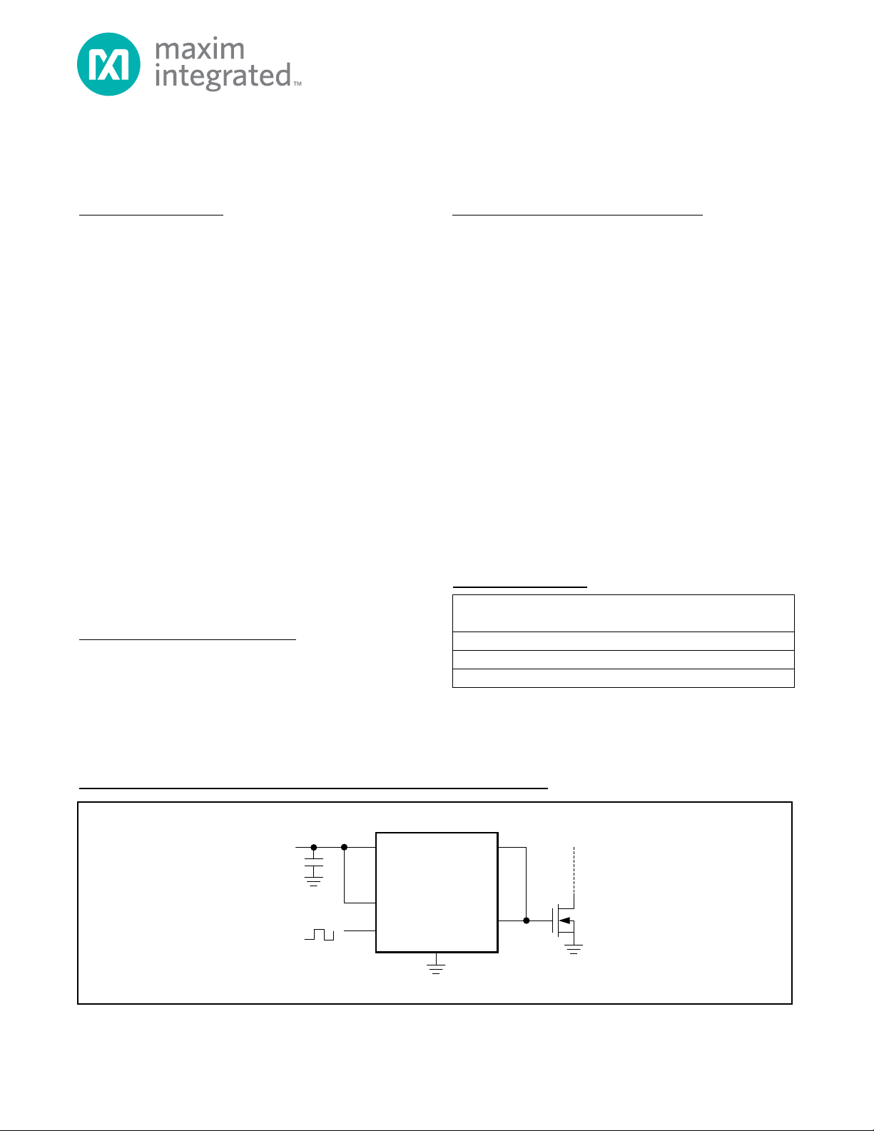
Typical Operating Circuit
V+V+
MAX15070A
MAX15070B
IN+
IN-
For pricing, delivery, and ordering information, please contact Maxim Direct
at 1-888-629-4642, or visit Maxim’s website at www.maximintegrated.com.
GND
P_OUT
N_OUT
N
19-5516; Rev 3; 5/13
Page 2
MAX15070A/MAX15070B
7A Sink, 3A Source,
12ns, SOT23 MOSFET Drivers
ABSOLUTE MAXIMUM RATINGS
(Voltages referenced to GND.)
V+, IN+, INN_OUT, P_OUT
N_OUT Continuous Output Current (Note 1)
P_OUT Continuous Output Current (Note 1)
Continuous Power Dissipation (T
SOT23 (derate 8.7mW/NC above +70NC)
*As per JEDEC 51 standard.
Note 1: Continuous output current is limited by the power dissipation of the package.
.......................................................... -0.3V to +16V
...........................................-0.3V to (V+ + 0.3V)
................. -200mA
................ +125mA
= +70NC)
A
.................. 696mW*
PACKAGE THERMAL CHARACTERISTICS (Note 2)
SOT23
Junction-to-Ambient Thermal Resistance (B
Junction-to-Case Thermal Resistance (B
Note 2: Package thermal resistances were obtained using the method described in JEDEC specification JESD51-7, using a four-lay-
er board. For detailed information on package thermal considerations, refer to www.maximintegrated.com/thermal-tutorial.
Stresses beyond those listed under “Absolute Maximum Ratings” may cause permanent damage to the device. These are stress ratings only, and functional
operation of the device at these or any other conditions beyond those indicated in the operational sections of the specifications is not implied. Exposure to absolute
maximum rating conditions for extended periods may affect device reliability.
) ........115NC/W
JA
) .................. 80NC/W
JC
Operating Temperature Range
Junction Temperature
Storage Temperature Range
Lead Temperature (soldering, 10s)
Soldering Temperature (reflow)
................................................... +150NC
...................... -40NC to +125NC
........................... -65NC to +150NC
......................................+260NC
................................+300NC
ELECTRICAL CHARACTERISTICS
(V+ = +12V, CL = 0F, TA = TJ = -40NC to +125NC, unless otherwise noted. Typical values are at TA = +25NC. Parameters specified at
V+ = +4.5V apply to the MAX15070A only; see Figure 1.) (Note 3)
PARAMETER SYMBOL CONDITIONS MIN TYP MAX UNITS
POWER SUPPLY (V+)
Input Voltage Range
Undervoltage Lockout V
Undervoltage-Lockout
Hysteresis
Undervoltage Lockout to Output
Rising Delay
Undervoltage Lockout to Output
Falling Delay
Supply Current I
n-CHANNEL OUTPUT (N_OUT)
N_OUT Resistance R
Power-Off Pulldown Resistance
Output Bias Current I
Peak Output Current I
UVLO
N_OUT
BIASNVN_OUT
PEAKNCL
MAX15070A 4 14
MAX15070B 6 14
V+ rising 3.3 3.45 3.6 V
200 mV
V+ rising 100
V+ falling 2
V+ = 14V, no switching 0.5 1
V+
V+ = 14V, switching at 1MHz 2.3
= +25NC
V+ = +12V,
I
= -100mA
N_OUT
V+ = +4.5V,
I
= -100mA
N_OUT
V+ = unconnected, I
= V+ 6 11
= 22nF 7.0 A
N_OUT
T
A
T
= +125NC
A
= +25NC
T
A
T
= +125NC
A
= -1mA, TA = +25NC
0.256 0.32
0.268 0.33
1.3 1.9
0.45
0.465
V
Fs
Fs
mA
I
kI
FA
2 Maxim Integrated
Page 3
MAX15070A/MAX15070B
7A Sink, 3A Source,
12ns, SOT23 MOSFET Drivers
ELECTRICAL CHARACTERISTICS (continued)
(V+ = +12V, CL = 0F, TA = TJ = -40NC to +125NC, unless otherwise noted. Typical values are at TA = +25NC. Parameters specified at
V+ = +4.5V apply to MAX15070A only, see Figure 1.) (Note 3)
PARAMETER SYMBOL CONDITIONS MIN TYP MAX UNITS
p-CHANNEL OUTPUT (P_OUT)
= +25NC
V+ = +12V,
I
= 100mA
P_OUT Resistance R
Output Leakage Current I
Peak Output Current I
LOGIC INPUTS (IN+, IN-)
Logic-High Input Voltage V
Logic-Low Input Voltage V
Logic-Input Hysteresis V
Logic-Input Leakage Current V
Logic-Input Bias Current V
Input Capacitance 10 pF
SWITCHING CHARACTERISTICS FOR V+ = +12V (Figure 1)
Rise Time t
Fall Time t
Turn-On Delay Time t
Turn-Off Delay Time t
Break-Before-Make Time t
SWITCHING CHARACTERISTICS FOR V+ = +4.5V (MAX15070A only) (Figure 1)
Rise Time t
Fall Time t
Turn-On Delay Time t
Turn-Off Delay Time t
Break-Before-Make Time t
THERMAL CHARACTERISTICS
Thermal Shutdown Temperature rising (Note 4) 166
Thermal-Shutdown Hysteresis (Note 4) 13
Note 3: Limits are 100% tested at T
the statistical quality control (SQC) method.
Note 4: Design guaranteed by bench characterization. Limits are not production tested.
P_OUT
LEAKPVP_OUT
PEAKNCL
D-ONCL
D-OFFCL
BBM
D-ONCL
D-OFFCL
BBM
= +25°C. Limits over operating temperature range are guaranteed through correlation using
A
P_OUT
V+ = +4.5V,
I
= 100mA
P_OUT
= 0V 0.01 1
= 22nF 3.0 A
MAX15070A 2.0
IH
MAX15070B 4.25
MAX15070A 0.8
IL
MAX15070B 2.0
MAX15070A 0.2
HYS
MAX15070B 0.9
= V
IN+
IN+
CL = 1nF 6
R
F
R
F
= 5nF 22
L
C
= 10nF 36
L
CL = 1nF 4
= 5nF 11
L
C
= 10nF 17
L
= 1nF (Note 4) 7 11 17 ns
= 1nF (Note 4) 7 12 18 ns
CL = 1nF 5
= 5nF 16
L
C
= 10nF 25
L
CL = 1nF 4
= 5nF 10
L
C
= 10nF 14
L
= 1nF (Note 4) 7 13 21 ns
= 1nF (Note 4) 7 14 22 ns
= 0V or V+, MAX15070A 0.02
IN-
= V
= 0V or V+, MAX15070B 10
IN-
T
A
T
= +125NC
A
= +25NC
T
A
T
= +125NC
A
0.88 1.2
1.7
0.91 1.25
1.75
2 ns
2 ns
I
FA
V
V
V
FA
nsC
nsC
nsC
nsC
NC
NC
3Maxim Integrated
Page 4
MAX15070A/MAX15070B
41
41
41
41
41
41
01
7A Sink, 3A Source,
12ns, SOT23 MOSFET Drivers
Typical Operating Characteristics
= 1000pF, T
(C
L
7.0
6.5
6.0
5.5
5.0
4.5
4.0
RISE TIME (ns)
3.5
3.0
2.5
2.0
TA = +125°C
= +25NC, unless otherwise noted. See Figure 1.)
A
RISE TIME vs. SUPPLY VOLTAGE
5.5
TA = +85°C
TA = +25°C
TA = 0°C
SUPPLY VOLTAGE (V)
TA = -40°C
121086
4
MAX15070A toc01
FALL TIME (ns)
5.0
4.5
4.0
3.5
3.0
2.5
2.0
1.5
FALL TIME vs. SUPPLY VOLTAGE
TA = +125°C
TA = +25°C
SUPPLY VOLTAGE (V)
TA = +85°C
TA = -40°C
TA = 0°C
12106 8
18
16
MAX15070A toc02
14
12
PROPAGATION DELAY (ns)
10
4
8
PROPAGATION DELAY (LOW TO HIGH)
vs. SUPPLY VOLTAGE
TA = +125°C
TA = +85°C
TA = +25°C
TA = 0°C
SUPPLY VOLTAGE (V)
TA = -40°C
121086
4
MAX15070A toc03
PROPAGATION DELAY (HIGH TO LOW)
vs. SUPPLY VOLTAGE
20
18
TA = +125°C
16
14
12
PROPAGATION DELAY (ns)
10
8
TA = +85°C
TA = +25°C
TA = 0°C
SUPPLY VOLTAGE (V)
SUPPLY CURRENT vs. TEMPERATURE
1.4
V+ = 12V
f = 100kHz, C
1.2
DUTY CYCLE = 50%
1.0
0.8
SUPPLY CURRENT (mA)
0.6
0.4
-40 125
= 0
L
TEMPERATURE (°C)
TA = -40°C
121086
1109580655035205-10-25
SUPPLY CURRENT vs. SUPPLY VOLTAGE
3.0
2.5
MAX15070A toc04
2.0
1.5
1.0
SUPPLY CURRENT (mA)
0.5
40kHz
4
MAX15070A toc07
0
4.0
3.5
3.0
2.5
2.0
1.5
1.0
INPUT THRESHOLD VOLTAGE (V)
0.5
0
DUTY CYCLE = 50%
CL = 0
75kHz
SUPPLY VOLTAGE (V)
1MHz
500kHz
100kHz
121086
MAX15070A INPUT THRESHOLD
VOLTAGE vs. SUPPLY VOLTAGE
RISING
FALLING
12106 8
SUPPLY VOLTAGE (V)
4.0
3.5
MAX15070A toc05
3.0
2.5
2.0
1.5
SUPPLY CURRENT (mA)
1.0
0.5
4
4
0
1.4
1.3
1.2
MAX15070A toc08
1.1
1.0
0.9
0.8
0.7
SUPPLY CURRENT (mA)
0.6
0.5
0.4
SUPPLY CURRENT vs. LOAD CAPACITANCE
V+ = 12V
f = 100kHz
DUTY CYCLE = 50%
0 2000
LOAD CAPACITANCE (pF)
16001200400 800
MAX15070A
SUPPLY CURRENT vs. INPUT VOLTAGE
INPUT LOW TO HIGH
INPUT HIGH TO LOW
54321
INPUT VOLTAGE (V)
MAX15070A toc06
MAX15070A toc09
4
4 Maxim Integrated
Page 5

MAX15070A/MAX15070B
7A Sink, 3A Source,
12ns, SOT23 MOSFET Drivers
Typical Operating Characteristics (continued)
= 1000pF, T
(C
L
= +25NC, unless otherwise noted. See Figure 1.)
A
INPUT VOLTAGE vs. OUTPUT VOLTAGE
(V+ = +4V, C
L
20ns/div
= 5000pF)
MAX15070A toc10
INPUT VOLTAGE vs. OUTPUT VOLTAGE
(V+ = +4V, C
= 10,000pF)
L
MAX15070A toc13
V
IN+
2V/div
V
OUTPUT
2V/div
V
IN+
2V/div
INPUT VOLTAGE vs. OUTPUT VOLTAGE
(V+ = +4V, C
= 10,000pF)
L
20ns/div
MAX15070A toc11
INPUT VOLTAGE vs. OUTPUT VOLTAGE
(V+ = +14V, C
= 5000pF)
L
MAX15070A toc14
V
IN+
2V/div
V
OUTPUT
2V/div
V
IN+
5V/div
V
OUTPUT
5V/div
INPUT VOLTAGE vs. OUTPUT VOLTAGE
(V+ = +4V, C
L
20ns/div
= 5000pF)
MAX15070A toc12
INPUT VOLTAGE vs. OUTPUT VOLTAGE
(V+ = +14V, C
= 10,000pF)
L
MAX15070A toc15
V
IN+
2V/div
V
OUTPUT
2V/div
V
IN+
5V/div
V
OUTPUT
5V/div
V
OUTPUT
2V/div
20ns/div
INPUT VOLTAGE vs. OUTPUT VOLTAGE
20ns/div
= 5000pF)
L
MAX15070A toc16
(V+ = +14V, C
V
IN+
5V/div
V
OUTPUT
5V/div
20ns/div
INPUT VOLTAGE vs. OUTPUT VOLTAGE
(V+ = +14V, C
= 10,000pF)
L
20ns/div
MAX15070A toc17
20ns/div
V
IN+
5V/div
V
OUTPUT
5V/div
5Maxim Integrated
Page 6
MAX15070A/MAX15070B
7A Sink, 3A Source,
12ns, SOT23 MOSFET Drivers
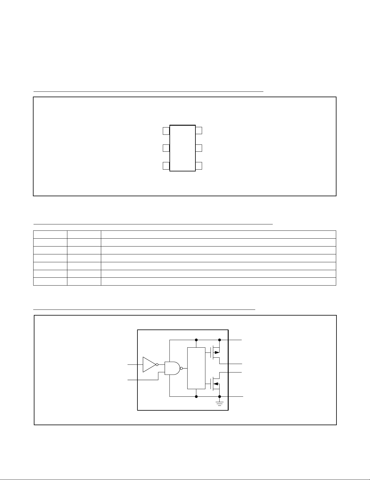
Pin Configuration
TOP VIEW
GND
IN-
1IN+
2
3
+
MAX15070A
MAX15070B
SOT23
6V+
5 P_OUT
N_OUT
4
Pin Description
PIN NAME FUNCTION
1 IN+ Noninverting Logic Input. Connect IN+ to V+ when not used.
2 GND Ground
3 IN- Inverting Logic Input. Connect IN- to GND when not used.
4 N_OUT Driver Sink Output. Open-drain n-channel output. Sinks current for power MOSFET turn-off.
5 P_OUT Driver Source Output. Open-drain p-channel output. Sources current for power MOSFET turn-on.
6 V+
Power-Supply Input. Bypass V+ to GND with a 1FF low-ESR ceramic capacitor.
Functional Diagram
V+
P
IN-
IN+
MAX15070A
MAX15070B
6 Maxim Integrated
BREAK-
BEFORE-
MAKE
CONTROL
P_OUT
N_OUT
N
GND
Page 7
MAX15070A/MAX15070B
7A Sink, 3A Source,
12ns, SOT23 MOSFET Drivers
IN+
V
IL
P_OUT AND
N_OUT
CONNECTED
TOGETHER
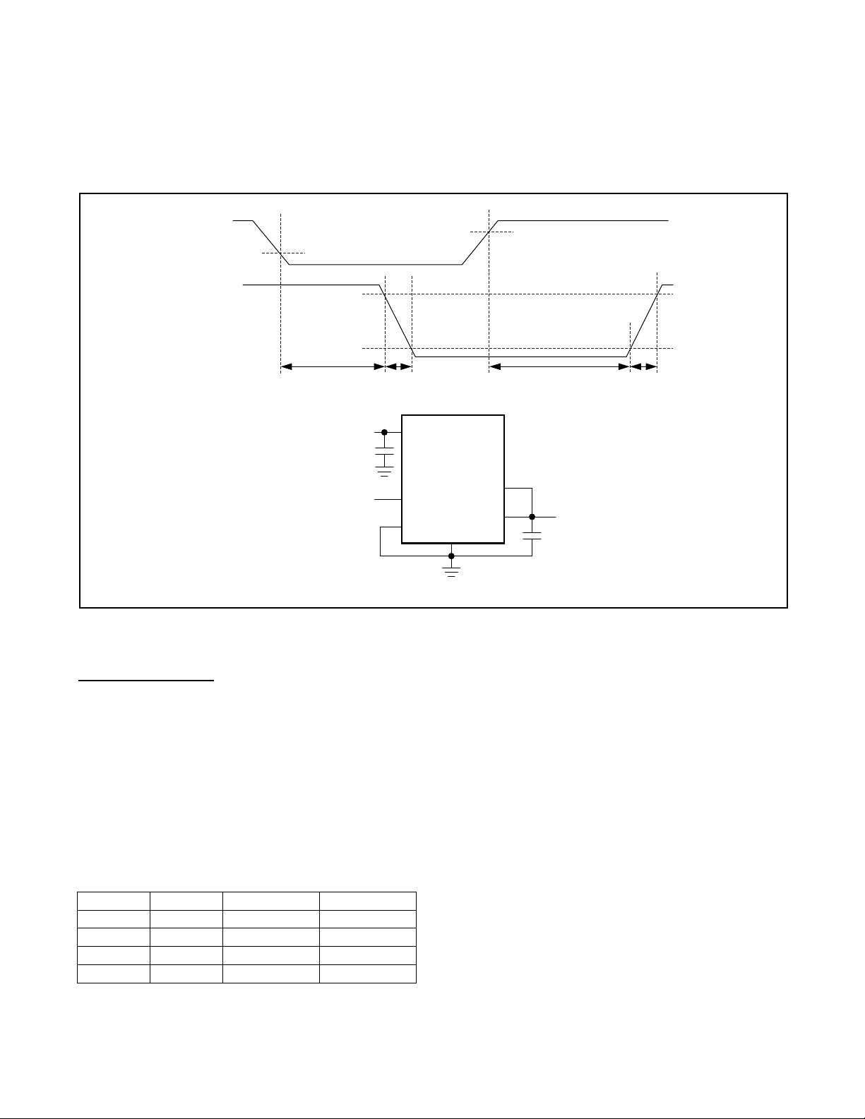
Figure 1. Timing Diagram and Test Circuit
t
D-OFF
90%
10%
INPUT
V
IH
C
t
D-ON
L
OUTPUT
t
R
t
F
TIMING DIAGRAM
V+
V+
MAX15070A
MAX15070B
IN+
IN-
TEST CIRCUIT
P_OUT
N_OUT
GND
Detailed Description
Logic Inputs
The MAX15070A/MAX15070Bs’ logic inputs are protected against voltage spikes up to +16V, regardless of
the V+ voltage. The low 10pF input capacitance of the
inputs reduces loading and increases switching speed.
These ICs have two inputs that give the user greater
flexibility in controlling the MOSFET. Table 1 shows all
possible input combinations. The difference between the
MAX15070A and the MAX15070B is the input threshold
voltage. The MAX15070A has TTL logic-level thresholds,
Table 1. Truth Table
IN+ IN- p-CHANNEL n-CHANNEL
L L Off On
L H Off On
H L On Off
H H Off On
L = Logic-low, H = Logic-high.
while the MAX15070B has HNM (CMOS-like) logic-level
thresholds (see the Electrical Characteristics). Connect
IN+ to V+ or IN- to GND when not used. Alternatively,
the unused input can be used as an on/off control input
(Table 1).
Undervoltage Lockout (UVLO)
When V+ is below the UVLO threshold, the n-channel is
on and the p-channel is off, independent of the state of
the inputs. The UVLO is typically 3.45V with 200mV typical hysteresis to avoid chattering. A typical falling delay
of 2Fs makes the UVLO immune to narrow negative transients in noisy environments.
Driver Outputs
The ICs provide two separate outputs. One is an opendrain p-channel, the other an open-drain n-channel. They
have distinct current sourcing/sinking capabilities to independently control the rise and fall times of the MOSFET
gate. Add a resistor in series with P_OUT/N_OUT to slow
the corresponding rise/fall time of the MOSFET gate.
7Maxim Integrated
Page 8

MAX15070A/MAX15070B
7A Sink, 3A Source,
12ns, SOT23 MOSFET Drivers
Applications Information
Supply Bypassing, Device
Grounding, and Placement
Ample supply bypassing and device grounding are
extremely important because when large external capacitive loads are driven, the peak current at the V+ pin can
approach 3A, while at the GND pin, the peak current can
approach 7A. V
negative feedback for inverters and, if excessive, can
cause multiple switching when the IN- input is used and
the input slew rate is low. The device driving the input
should be referenced to the ICs’ GND pin, especially
when the IN- input is used. Ground shifts due to insufficient device grounding can disturb other circuits sharing
the same AC ground return path. Any series inductance
in the V+, P_OUT, N_OUT, and/or GND paths can cause
oscillations due to the very high di/dt that results when
the ICs are switched with any capacitive load. A 1FF
or larger value ceramic capacitor is recommended,
bypassing V+ to GND and placed as close as possible
to the pins. When driving very large loads (e.g., 10nF)
at minimum rise time, 10FF or more of parallel storage
capacitance is recommended. A ground plane is highly
recommended to minimize ground return resistance and
series inductance. Care should be taken to place the
ICs as close as possible to the external MOSFET being
driven to further minimize board inductance and AC path
resistance.
Power dissipation of the ICs consists of three components, caused by the quiescent current, capacitive
charge and discharge of internal nodes, and the output
current (either capacitive or resistive load). The sum of
these components must be kept below the maximum
power-dissipation limit of the package at the operating
temperature.
The quiescent current is 0.5mA typical. The current
required to charge and discharge the internal nodes
is frequency dependent (see the Typical Operating
Characteristics).
For capacitive loads, the total power dissipation is
approximately:
where C
voltage, and FREQ is the switching frequency.
LOAD
drops and ground shifts are forms of
CC
Power Dissipation
P = C
is the capacitive load, V+ is the supply
x (V+) 2 x FREQ
LOAD
Layout Information
The ICs’ MOSFET drivers source and sink large currents
to create very fast rise and fall edges at the gate of the
switching MOSFET. The high di/dt can cause unacceptable ringing if the trace lengths and impedances are not
well controlled. The following PCB layout guidelines are
recommended when designing with the ICs:
• Place one or more 1FF decoupling ceramic
capacitor(s) from V+ to GND as close as possible to
the IC. At least one storage capacitor of 10FF (min)
should be located on the PCB with a low resistance
path to the V+ pin of the ICs. There are two AC current loops formed between the IC and the gate of
the MOSFET being driven. The MOSFET looks like
a large capacitance from gate to source when the
gate is being pulled low. The active current loop is
from N_OUT of the ICs to the MOSFET gate to the
MOSFET source and to GND of the ICs. When the
gate of the MOSFET is being pulled high, the active
current loop is from P_OUT of the ICs to the MOSFET
gate to the MOSFET source to the GND terminal of
the decoupling capacitor to the V+ terminal of the
decoupling capacitor and to the V+ terminal of the
ICs. While the charging current loop is important, the
discharging current loop is critical. It is important to
minimize the physical distance and the impedance
in these AC current paths.
• In a multilayer PCB, the component surface layer surrounding the ICs should consist of a GND plane containing the discharging and charging current loops.
Chip Information
Process: BiCMOS
Package Information
For the latest package outline information and land patterns
(footprints), go to www.maximintegrated.com/packages. Note
that a “+”, “#”, or “-” in the package code indicates RoHS status
only. Package drawings may show a different suffix character,
but the drawing pertains to the package regardless of RoHS
status.
PACKAGE
TYPE
6 SOT23 U6+1
PACKAGE
CODE
OUTLINE
NO.
21-0058 90-0175
LAND
PATTERN NO.
8 Maxim Integrated
Page 9

MAX15070A/MAX15070B
7A Sink, 3A Source,
12ns, SOT23 MOSFET Drivers
Revision History
REVISION
NUMBER
0 11/10 Initial release —
1 11/11 Added MAX15070AAVT/V+ to data sheet 1, 2, 3, 8, 9
2 8/12 Removed Evaluation Kit Available banner 1
3 5/13 Updated Ordering Information 1
REVISION
DATE
DESCRIPTION
PAGES
CHANGED
Maxim cannot assume responsibility for use of any circuitry other than circuitry entirely embodied in a Maxim product. No circuit patent licenses are implied.
Maxim reserves the right to change the circuitry and specifications without notice at any time. The parametric values (min and max limits) shown in the Electrical
Characteristics table are guaranteed. Other parametric values quoted in this data sheet are provided for guidance.
Maxim Integrated 160 Rio Robles, San Jose, CA 95134 USA 1-408-601-1000 9
©
2013 Maxim Integrated Products, Inc. The Maxim logo and Maxim Integrated are trademarks of Maxim Integrated Products, Inc.
Page 10

 Loading...