Maxim MAX15032 Datasheet

General Description
The MAX15032 constant-frequency, pulse-width-modulating (PWM), low-noise boost converter is intended for
low-voltage systems that need a locally generated high
voltage. This device is capable of generating low-noise,
high output voltages, with an output power capability
up to 600mW with a 2.9V input voltage. This device can
be used for a wide variety of applications, such as PIN
or varactor diode biasing and LCD displays. The
MAX15032 operates from +2.7V to +11V.
The constant-frequency (500kHz), current-mode PWM
architecture provides low-noise output voltage that is
easy to filter. A high-voltage internal lateral DMOS
power switch allows this device to boost output voltages up to 36V. The MAX15032 features a shutdown
mode to save power.
The MAX15032 is available in a small thermally
enhanced 3mm x 3mm 8-pin TDFN package and is
specified for operation over the -40°C to +125°C automotive temperature range.
Applications
Avalanche Photodiode Biasing
PIN Diode Bias Supplies
Low-Noise Varactor Diode Bias Supplies
STB Audio IC Supplies
LCD Displays
Features
o Input Voltage Range
+2.7V to +5.5V (Using Internal Charge Pump)
+5.5V to +11V
o Wide Adjustable Output Voltage Range: (V
IN
+ 1V)
to 36V
o Output Power: ≥ 600mW for V
IN
≥ 2.9V
o Internal 0.5Ω (typ), 40V Switch
o Constant PWM Frequency Provides Easy Filtering
in Low-Noise Applications
o 500kHz (typ) Switching Frequency
o 0.5µA (max) Shutdown Current
o Internal Soft-Start
o Small Thermally Enhanced 3mm x 3mm 8-Pin
TDFN Package
MAX15032
500kHz, 36V Output, 600mW PWM
Step-Up DC-DC Converter
________________________________________________________________
Maxim Integrated Products
1
1
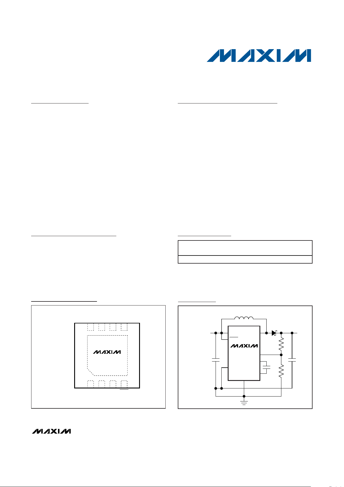
+
34
865
PGND CN IN
MAX15032
2
7
CP
LX FB SHDNGND
TDFN
TOP VIEW
Pin Configuration
Ordering Information
MAX15032
INVIN = 2.7V TO 5.5V
V
OUT
36V
SHDN
PGND
LX
FB
CP
CN
GND
R1
D1
L1
R2
C
IN
C
OUT
C
CP
Typical Operating Circuit
19-4232; Rev 0; 8/08
For pricing, delivery, and ordering information, please contact Maxim Direct at 1-888-629-4642,
or visit Maxim’s website at www.maxim-ic.com.
PART
TEMP RANGE
PIN-
PACKAGE
TOP
MARK
MAX15032ATA+T
-40°C to +125°C 8 TDFN-EP*
+BKP
+
Denotes a lead-free/RoHS-compliant package.
T = Tape and reel.
*
EP = Exposed pad.

MAX15032
500kHz, 36V Output, 600mW PWM
Step-Up DC-DC Converter
2 _______________________________________________________________________________________
ABSOLUTE MAXIMUM RATINGS
ELECTRICAL CHARACTERISTICS
(VIN= +3.3V, V
SHDN
= +3.3V, CIN= 10µF, PGND = GND = 0V, TA= TJ= -40°C to +125°C, unless otherwise noted. Typical values
are at T
A
= +25°C. See the
Typical Operating Circuit
.) (Note 2)
Stresses beyond those listed under “Absolute Maximum Ratings” may cause permanent damage to the device. These are stress ratings only, and functional
operation of the device at these or any other conditions beyond those indicated in the operational sections of the specifications is not implied. Exposure to
absolute maximum rating conditions for extended periods may affect device reliability.
Note 1: Package thermal resistances were obtained using the method described in JEDEC specification JESD51-7, using a four-
layer board. For detailed information on package thermal considerations, refer to www.maxim-ic.com/thermal-tutorial.
IN to GND ...............................................................-0.3V to +12V
LX to PGND ............................................................-0.3V to +40V
FB to GND ..............................................................-0.3V to +12V
SHDN to GND..............................................-0.3V to (V
IN
+ 0.3V)
CN to GND .............................................................-0.3V to +12V
CP to GND..............................................................-0.3V to +12V
PGND to GND .......................................................-0.3V to +0.3V
Continuous Power Dissipation (T
A
= +70°C)
8-Pin TDFN (derate 24.4mW/°C above +70°C) ......1951.2mW
Junction-to-Case Thermal Resistance (θ
JC
) (Note 1) ........8°C/W
Junction-to-Ambient Thermal Resistance (θ
JA
)
(Note 1) ........................................................................41°C/W
Operating Temperature Range .........................-40°C to +125°C
Junction Temperature......................................................+150°C
Storage Temperature Range .............................-65°C to +150°C
Lead Temperature (soldering, 10s) .................................+300°C
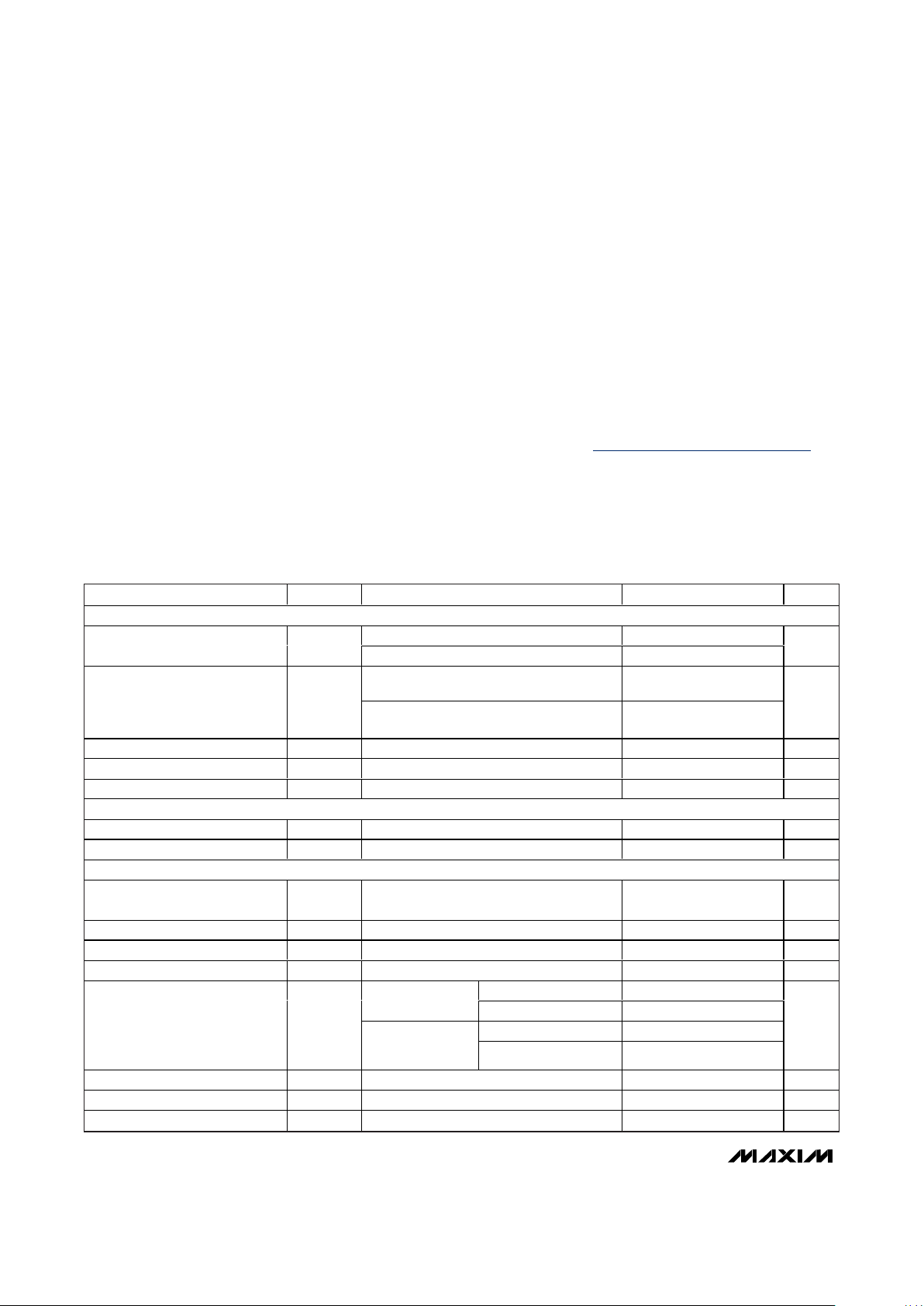
PARAMETER SYMBOL CONDITIONS MIN TYP MAX UNITS
SUPPLY VOLTAGE
CCP = 10nF 2.7 5.5
Supply Voltage Range V
IN
CP connected to IN 5.5 11
V
VFB = 1.4V (no switching), CCP = 10nF,
V
IN
= 3.3V
12
Supply Current I
IN
VFB = 1.4V (no switching), CP = IN,
V
IN
= 11V
1.5 3
mA
Undervoltage Lockout V
UVLO
VIN rising 2.375 2.5 2.675 V
Undervoltage Lockout Hysteresis V
UVLO-HYS
100 mV
Shutdown Current I
SHDN
V
SHDN
= 0V 0.5 µA
LOGIC INPUT (SHDN)
SHDN Input Low Level V
IL
0.8 V
SHDN Input High Level V
IH
2.0 V
BOOST CONVERTER
Output Voltage Adjustment
Range
V
IN
+ 1 36 V
Switching Frequency f
SW
450 500 550 kHz
FB Set Point V
FB
1.214 1.245 1.276 V
FB Input Bias Current I
FB
300 nA
VIN = 2.9V, VCP = 5.5V 0.42 1
CCP = 10nF,
I
LX
= 100mA
V
IN
= 5.5V, VCP = 10V 0.33 1
VIN = VCP = 5.5V 0.42 1
LX Switch On-Resistance R
DS_ON
CP connected to
IN, I
LX
= 100mA
V
IN
= VCP = 11V 0.33 1
Ω
Peak Switch Current Limit I
LIM_LX
1 1.33 1.7 A
LX Leakage Current VLX = 36V 2 µA
Line Regulation I
LOAD
= 2mA 0.25 %

MAX15032
500kHz, 36V Output, 600mW PWM
Step-Up DC-DC Converter
_______________________________________________________________________________________ 3
Note 2: All devices are 100% production tested at room temperature (TA= +25°C). All parameter limits through the temperature
range are guaranteed by design.
PARAMETER SYMBOL CONDITIONS MIN TYP MAX UNITS
Load Regulation I
LOAD
= 0 to 20mA, V
OUT
= 30V 1 %
Soft-Start Duration 8ms
Soft-Start Steps (0.25 x I
LIM_LX
) to I
LIM_LX
32 Steps
THERMAL PROTECTION
Thermal Shutdown Rising +160 °C
Thermal-Shutdown Hysteresis 8°C
ELECTRICAL CHARACTERISTICS (continued)
(VIN= +3.3V, V
SHDN
= +3.3V, CIN= 10µF, PGND = GND = 0V, TA= TJ= -40°C to +125°C, unless otherwise noted. Typical values
are at T
A
= +25°C. See the
Typical Operating Circuit
.) (Note 2)
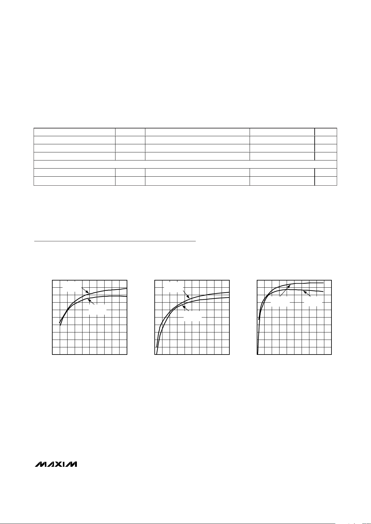
EFFICIENCY
vs. LOAD CURRENT
MAX15032 toc01
LOAD CURRENT (mA)
EFFICIENCY (%)
181612 144 6 8 102
40
45
50
55
60
65
70
75
80
85
35
020
V
OUT
= 36V
V
IN
= 5V
V
OUT
= 36V
V
IN
= 3.3V
EFFICIENCY
vs. LOAD CURRENT
MAX15032 toc02
LOAD CURRENT (mA)
EFFICIENCY (%)
181612 144 6 8 102
40
45
50
55
60
65
70
75
80
85
35
020
V
OUT
= 30V
V
IN
= 5V
V
OUT
= 30V
V
IN
= 3.3V
EFFICIENCY
vs. LOAD CURRENT
MAX15032 toc03
LOAD CURRENT (mA)
EFFICIENCY (%)
454030 3510 15 20 255
40
45
50
55
60
65
70
75
80
85
35
050
V
OUT
= 24V
V
IN
= 5V
V
OUT
= 24V
V
IN
= 3.3V
Typical Operating Characteristics
(VIN= 3.3V, L1 = 4.7µH, R1 = 143kΩ, R2 = 6.2kΩ, CIN= 10µF, C
OUT
= 2.2µF, CCP= 10nF, see the
Typical Operating Circuit
.
TA= +25°C, unless otherwise noted.)
 Loading...