

Page 1
19-5965; Rev 0; 6/11
MAX14950A
Single-Lane PCIe Equalizer/Redriver
General Description
The MAX14950A dual equalizer/redriver improves PCI
Express® (PCIe) signal integrity by providing programmable input equalization. This feature reduces deterministic jitter and redrives circuitry to reestablish deemphasis, which compensates for circuit-board loss at high
frequencies. The device permits optimal placement of
key PCIe components and allows for longer runs of stripline, microstrip, or cable.
The device contains two identical channels capable
of equalizing PCIe Gen III (8GT/s), Gen II (5GT/s), and
Gen I (2.5GT/s) signals and features electrical idle and
receiver detection.
The MAX14950A is available in a small, 40-pin, 5.0mm
x 5.0mm TQFN package with flow-through traces for
optimal layout and minimal space requirements. It is
specified over the 0NC to +70NC commercial operating
temperature range.
Applications
Servers
Industrial PCs
Test Equipment
Computers
External Graphics Applications
Communications Switchers
Storage Area Networks
Benefits and Features
S Innovative Design Eliminates Need for Costly
External Components
Single +3.3V Supply Operation
S Increased Design Flexibility for Backward-
Compatible Applications
Optimized for PCIe Gen III (8GT/s) and
Gen II (5GT/s) Signals and Compatible with
Gen I (2.5GT/s) Signals
S High Level of Integration for Performance
Very Low Latency With 160ps (typ) Propagation
Delay
PCIe Gen III (8GT/s)-Compliant Input/Output
Return Loss
Four-Level-Programmable Input Equalization
Eight-Level-Programmable Output Emphasis
Electrical Idle Detection
Receiver Detection Permits Completely
Transparent Operation
S Ideal for Space-Sensitive Applications
On-Chip 50I Input/Output Terminations
40-Pin, 5.0mm x 5.0mm TQFN Packaging
Ordering Information appears at end of data sheet.
For related parts and recommended products to use with this part,
refer to www.maxim-ic.com/MAX14950A.related.
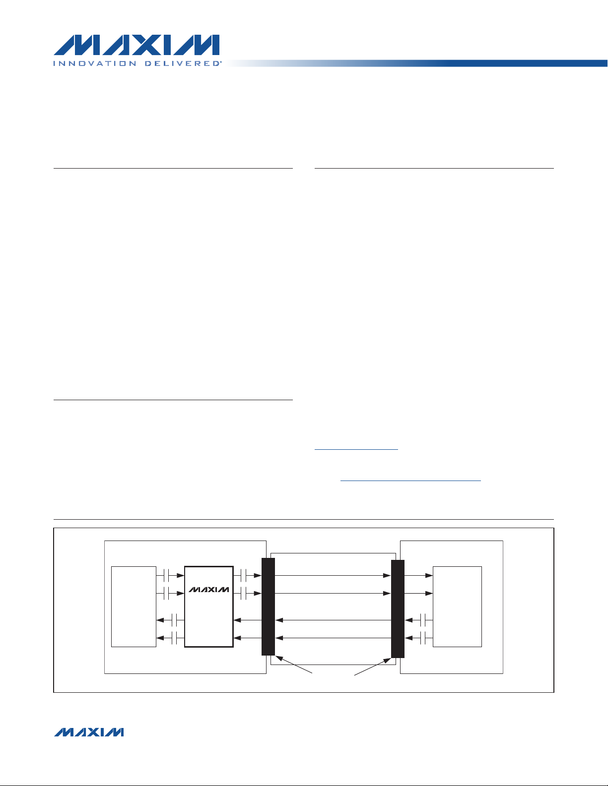
Typical Operating Circuit
MAIN BOARD
Tx
PCIe
Rx
PCI Express is a registered service mark of PCI-SIG Corporation.
����������������������������������������������������������������� Maxim Integrated Products 1
MAX14950A
MIDPLANE
SINGLE DIFFERENTIAL PAIR
SINGLE DIFFERENTIAL PAIR
CONNECTORS
REMOTE BOARD
Rx
PCIe
Tx
For pricing, delivery, and ordering information, please contact Maxim Direct at 1-888-629-4642,
or visit Maxim’s website at www.maxim-ic.com.
Page 2
MAX14950A
Single-Lane PCIe Equalizer/Redriver
ABSOLUTE MAXIMUM RATINGS
(Voltages referenced to GND.)
VCC ....................................................................... -0.3V to +4.0V
All Other Pins (Note 1) ............................. -0.3V to (VCC + 0.3V)
Continuous Current IN_P, IN_M,
OUT_P, OUT_M ........................................................... Q30mA
Peak Current IN_P, IN_M, OUT_P, OUT_M
(pulsed for 1Fs, 1% duty cycle) ................................ Q100mA
Note 1: All I/O pins are clamped by internal diodes.
Stresses beyond those listed under “Absolute Maximum Ratings” may cause permanent damage to the device. These are stress ratings only, and functional operation of the device at these or any other conditions beyond those indicated in the operational sections of the specifications is not implied. Exposure to absolute
maximum rating conditions for extended periods may affect device reliability.
PACKAGE THERMAL CHARACTERISTICS (Note 2)
TQFN
Junction-to-Ambient Thermal Resistance (BJA) ......... 28NC/W
Junction-to-Case Thermal Resistance (BJC) .................2NC/W
Note 2: Package thermal resistances were obtained using the method described in JEDEC specification JESD51-7, using a four-
layer board. For detailed information on package thermal considerations, refer to www.maxim-ic.com/thermal-tutorial.
Continuous Power Dissipation (TA = +70NC)
TQFN (derate 35.7mW/NC above +70NC)..................2857mW
Operating Temperature Range ............................. 0NC to +70NC
Junction Temperature Range ........................... -40NC to +150NC
Storage Temperature Range ............................ -65NC to +150NC
Lead Temperature (soldering, 10s) ................................+300NC
Soldering Temperature (reflow) ......................................+260NC
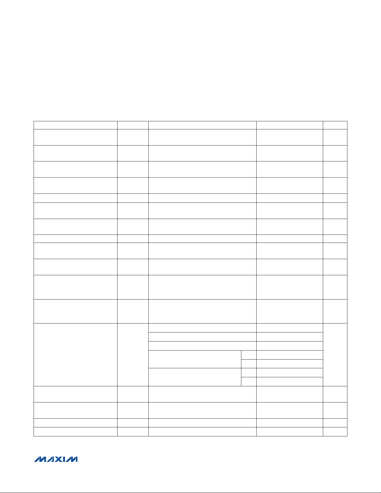
ELECTRICAL CHARACTERISTICS
(VCC = +3.0V to +3.6V, C
erwise noted. Typical values are at VCC = +3.3V and TA = +25NC.) (Note 3)
PARAMETER SYMBOL CONDITIONS MIN TYP MAX UNITS
DC PERFORMANCE
Power-Supply Range V
Supply Current I
= 200nF coupling capacitor on each output, RL = 50I on each output, TA = 0NC to +70NC, unless oth-
CL
CC
OEQ_2 = OEQ_1 = OEQ_0
= GND
OEQ_2 = OEQ_1 = GND,
OEQ_0 = V
OEQ_2 = OEQ_0 = GND,
OEQ_1 = V
OEQ_2 = GND, OEQ_1 =
CC
EN = V
OEQ_0 = V
CC
OEQ_2 = VCC, OEQ_1 =
OEQ_0 = GND
OEQ_2 = OEQ_0 = VCC,
OEQ_1 = GND
OEQ_2 = OEQ_1 = VCC,
OEQ_0 = GND
OEQ_2 = OEQ_1 = OEQ_0
= V
CC
CC
CC
CC
3.0 3.3 3.6 V
102 135
106 140
107 140
125 160
mA
106 140
132 170
140 180
165 210
����������������������������������������������������������������� Maxim Integrated Products 2
Page 3
Single-Lane PCIe Equalizer/Redriver
ELECTRICAL CHARACTERISTICS (continued)
(VCC = +3.0V to +3.6V, C
erwise noted. Typical values are at VCC = +3.3V and TA = +25NC.) (Note 3)
PARAMETER SYMBOL CONDITIONS MIN TYP MAX UNITS
Standby Current I
Differential Input Impedance
Differential Output Impedance
Common-Mode Resistance to
GND, Input Termination Not
Powered
= 200nF coupling capacitor on each output, RL = 50I on each output, TA = 0NC to +70NC, unless oth-
CL
OEQ_2 = OEQ_1 = OEQ_0
= GND
OEQ_2 = OEQ_1 = GND,
OEQ_0 = V
OEQ_2 = OEQ_0 = GND,
OEQ_1 = VCC
OEQ_2 = GND, OEQ_1 =
STBY
EN = GND
OEQ_0 = V
OEQ_2 = VCC, OEQ_1 =
OEQ_0 = GND
OEQ_2 = OEQ_0 = VCC,
OEQ_1 = GND
OEQ_2 = OEQ_1 = VCC,
OEQ_0 = GND
OEQ_2 = OEQ_1 = OEQ_0
= V
CC
Z
RX-DIFF-
DC
Z
TX-DIFF-
DC
Z
RX-HIGH-
IMP-DC
DC 80 100 120
DC 80 100 120
-150mV P V
IN_CM
P +200mV
CC
CC
MAX14950A
57 80
61 85
62 85
75 100
62 80
85 110
92 120
120 150
50
mA
I
I
kI
Common-Mode Resistance to
GND, Input Termination Powered
Output Short-Circuit Current I
Common-Mode Delta, Between
Active and Idle States
DC Output Offset, During Active
State
DC Output Offset, During
Electrical Idle
����������������������������������������������������������������� Maxim Integrated Products 3
Z
RX-DC
TX-SHORT
V
TX-CMDC-ACTIVEIDLE-DELTA
V
TXACTIVEDIFF-DC
V
TX-IDLE-
DIFF-DC
20 25 30
I
Single-ended (Note 4) 90 mA
100 mV
|(V
|(V
OUT_P
OUT_P
- V
- V
)| 50 mV
OUT_M
)| 50 mV
OUT_M
Page 4
Single-Lane PCIe Equalizer/Redriver
ELECTRICAL CHARACTERISTICS (continued)
(VCC = +3.0V to +3.6V, C
erwise noted. Typical values are at VCC = +3.3V and TA = +25NC.) (Note 3)
PARAMETER SYMBOL CONDITIONS MIN TYP MAX UNITS
AC PERFORMANCE (Note 4)
Input Return Loss, Differential RL
Input Return Loss, Common
Mode
Output Return Loss, Differential RL
Output Return Loss, Common
Mode
Redriver-Operation Differential
Input-Signal Range
Full-Swing Differential Output
Voltage (No Deemphasis)
Output Deemphasis Ratio, 0dB
Output Deemphasis Ratio, 3.5dB
Output Deemphasis Ratio, 6dB
Output Deemphasis Ratio, 6dB
with Higher Amplitude
Output Deemphasis Ratio, 3.5dB
with Preshoot
Output Deemphasis Ratio, 6dB
with Preshoot
Output Deemphasis Ratio, 9dB
with Preshoot
Output Deemphasis Ratio,
9dB with Preshoot and Higher
Amplitude
Input Equalization, 3dB
= 200nF coupling capacitor on each output, RL = 50I on each output, TA = 0NC to +70NC, unless oth-
CL
f = 0.05GHz to 1.25GHz 10 dB
RX-DIFF
f = 1.25GHz to 2.5GHz 8 dB
f = 2.5GHz to 4GHz 5 dB
RL
RX-CM
f = 0.05GHz to 2.5GHz 6 dB
f = 2.5GHz to 4GHz 4 dB
f = 0.05GHz to 1.25GHz 10 dB
TX-DIFF
f = 1.25GHz to 2.5GHz 8 dB
f = 2.5GHz to 4GHz 4 dB
RL
TX-CM
V
RX-DIFF-
PP
V
TX-DIFF-
PP
V
TX-DE-
RATIO-0dB
V
TX-DE-
RATIO-
3.5dB
V
TX-DE-
RATIO-6dB
V
TX-DE-HA-
RATIO-6dB
V
TX-DE-
PS-RATIO-
3.5dB
V
TX-DE-PS-
RATIO-6dB
V
TX-DE-PS-
RATIO-9dB
V
TX-DE-PS-
HA-RATIO-
9dB
V
RX-EQ-
3dB
f = 0.05GHz to 2.5GHz 6 dB
f = 2.5GHz to 4GHz 4 dB
2 x |(V
OUT_P
- V
OUT_M
)|,
OEQ_2 = OEQ_1 = OEQ_0 = GND
OEQ_2 = OEQ_1 = OEQ_0 = GND,
Figure 1
OEQ_2 = OEQ_1 = GND, OEQ_0 = VCC,
Figure 1
OEQ_2 = OEQ_0 = GND, OEQ_1 = VCC,
Figure 1
OEQ_2 = GND, OEQ_1 = OEQ_0 = VCC,
Figure 1
OEQ_2 = VCC, OEQ_1 = OEQ_0 = GND,
Figure 1
OEQ_2 = OEQ_0 = VCC, OEQ_1 = GND,
Figure 1
OEQ_2 = OEQ_1 = VCC, OEQ_0 = GND,
Figure 1
OEQ_2 = OEQ_1 = OEQ_0 = VCC,
Figure 1
INEQ_1 = INEQ_0 = GND (Note 5) 3 dB
MAX14950A
100 1200 mV
800 1000 1300 mV
0 dB
3.5 dB
6 dB
6 dB
3.5 dB
6 dB
9 dB
9 dB
P-P
P-P
����������������������������������������������������������������� Maxim Integrated Products 4
Page 5
MAX14950A
Single-Lane PCIe Equalizer/Redriver
ELECTRICAL CHARACTERISTICS (continued)
(VCC = +3.0V to +3.6V, C
erwise noted. Typical values are at VCC = +3.3V and TA = +25NC.) (Note 3)
PARAMETER SYMBOL CONDITIONS MIN TYP MAX UNITS
Input Equalization, 5dB
Input Equalization, 7dB
Input Equalization, 9dB
Output Common-Mode Voltage
Propagation Delay t
Rise/Fall Time
Rise/Fall Time Mismatch
Output Skew Same Pair t
Deterministic Jitter t
Random Jitter t
Electrical Idle Entry Delay
Electrical Idle Exit Delay
Electrical Idle Detect Threshold
(Note 7)
Output Voltage During Electrical
Idle (AC)
Receiver-Detect Pulse Amplitude
Receiver-Detect Pulse Width 100 ns
Receiver-Detect Retry Period 200 ns
= 200nF coupling capacitor on each output, RL = 50I on each output, TA = 0NC to +70NC, unless oth-
CL
V
RX-EQ-
5dB
V
RX-EQ-
7dB
V
RX-EQ-
9dB
V
TX-CM-
AC-PP
PD
t
TX-RISE-
FALL
t
TX-RF-
MISMATCH
SK
TX-DJ-DD
TX-RJ-DD
t
TX-IDLESET-TO-
IDLE
t
TX-IDLE-
TO-DIFF-
DATA
INEQ_1 = GND, INEQ_0 = V
(Note 5) 5 dB
CC
INEQ_1 = VCC, INEQ_0 = GND (Note 5) 7 dB
INEQ_1 = INEQ_0 = V
MAX(V
V
OUT_M
OUT_P
)/2
+ V
OUT_M
(Note 5) 9 dB
CC
)/2 - MIN(V
OUT_P
+
100 mV
120 160 240 ps
(Note 6) 20 ps
(Note 6) 3 ps
5 ps
K28.5 pattern, AC-coupled, RL = 50I, no
deemphasis, no preshoot, data rate = 8GT/s
D10.2 pattern, no deemphasis, no
preshoot, data rate = 8GT/s
From input to output, D10.2 pattern, data
rate = 1GT/s
From input to output, D10.2 pattern, data
rate = 1GT/s
10.5 23.5 ps
1.5 ps
5 ns
5 ns
EIL_L = EIH_H = EIH_L = GND 65 175
V
TX-IDLE-
THRESH
V
TX-IDLE-
DIFF-AC-P
V
TX-RCV-
DETECT
EIL_L = EIH_L = GND, EIH_H = V
EIL_L = EIH_H = GND, EIH_L = V
CC
CC
EIL_L = VCC, EIH_H = EIH_L = GND
EIL_L = EIH_H = VCC, EIH_L = GND
|(V
OUT_P
- V
)| 20 mV
OUT_M
Voltage change in positive direction 600 mV
85 215
25 155
V
V
V
V
50 175
IH
20 165
IL
80 205
IH
50 195
IL
mV
P-P
P-P
RMS
P-P
P-P
����������������������������������������������������������������� Maxim Integrated Products 5
Page 6
MAX14950A
Single-Lane PCIe Equalizer/Redriver
ELECTRICAL CHARACTERISTICS (continued)
(VCC = +3.0V to +3.6V, C
erwise noted. Typical values are at VCC = +3.3V and TA = +25NC.) (Note 3)
PARAMETER SYMBOL CONDITIONS MIN TYP MAX UNITS
CONTROL LOGIC
Input-Logic Level Low V
Input-Logic Level High V
Input-Logic Hysteresis V
Input Pulldown Resistance R
ESD PROTECTION
ESD Voltage Human Body Model (HBM) ±4 kV
Note 3: All devices are 100% production tested at TA = +70NC. Specifications over operating temperature range are guaranteed
by design.
Note 4: Guaranteed by design, unless otherwise noted.
Note 5: Equivalent to same amount of deemphasis driving the input.
Note 6: Rise and fall times are measured using 20% and 80% levels.
Note 7: Electrical idle detect threshold is measured using D10.2 pattern and data rate = 1GT/s.
= 200nF coupling capacitor on each output, RL = 50I on each output, TA = 0NC to +70NC, unless oth-
CL
IL
IH
HYST
PD
1.4 V
0.1 V
200 375 kI
0.6 V
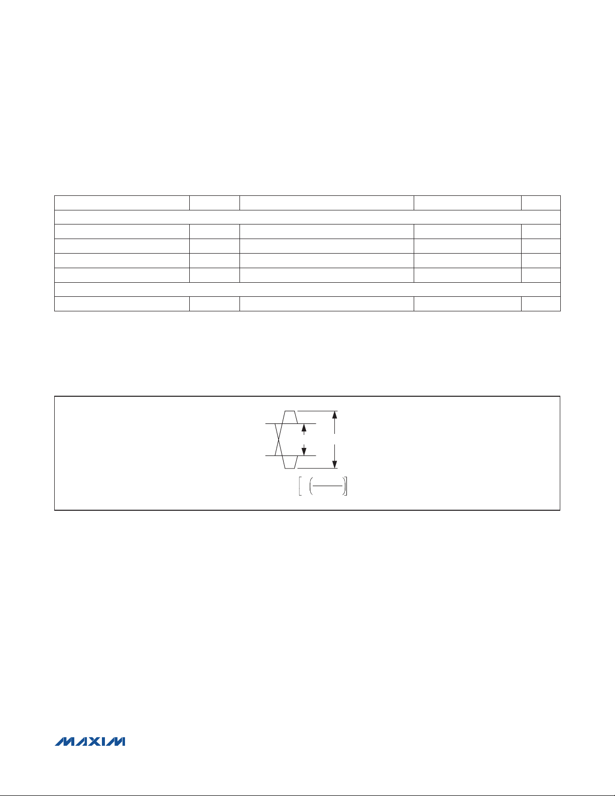
Figure 1. Illustration of Output Deemphasis
V
LOW_P-P
DE(dB) = 20 log
V
V
HIGH_P- P
V
LOW_P-P
HIGH_P-P
����������������������������������������������������������������� Maxim Integrated Products 6
Page 7

Single-Lane PCIe Equalizer/Redriver
(VCC = +3.3V, TA = +25NC, unless otherwise noted.)
MAX14950A
Typical Operating Characteristics
DATA RATE = 5Gbps,
INEQ_0 = INEQ_1 = 0, V
0EQ_0 = 0, OEQ_1 = 0, OEQ_2 = 0
600
400
200
0
VOLTAGE (mV)
-200
-400
-600
-200 150100500-50-100-150
TIME (ps)
DATA RATE = 5Gbps,
INEQ_0 = INEQ_1 = 0, V
0EQ_0 = 0, OEQ_1 = 0, OEQ_2 = 0
600
400
200
0
VOLTAGE (mV)
-200
-400
-600
-200 150100500-50-100-150
TIME (ps)
= 200mV
IN
= 200mV
IN
P-P
P-P
,
,
MAX14950A toc01
MAX14950A toc04
DATA RATE = 5Gbps,
INEQ_0 = INEQ_1 = 0, V
0EQ_0 = 0, OEQ_1 = 0, OEQ_2 = 0
600
400
200
0
VOLTAGE (mV)
-200
-400
-600
-200 150100500-50-100-150
TIME (ps)
DATA RATE = 5Gbps,
INEQ_0 = INEQ_1 = 0, V
0EQ_0 = 0, OEQ_1 = 0, OEQ_2 = 0
600
400
200
0
VOLTAGE (mV)
-200
-400
-600
-200 150100500-50-100-150
TIME (ps)
= 200mV
IN
= 200mV
IN
P-P
P-P
,
,
MAX14950A toc02
MAX14950A toc05
DATA RATE = 5Gbps,
INEQ_0 = INEQ_1 = 0, V
0EQ_0 = 0, OEQ_1 = 0, OEQ_2 = 0
600
400
200
0
VOLTAGE (mV)
-200
-400
-600
-200 150100500-50-100-150
TIME (ps)
DATA RATE = 5Gbps,
INEQ_0 = INEQ_1 = 0, V
0EQ_0 = 0, OEQ_1 = 0, OEQ_2 = 0
600
400
200
0
VOLTAGE (mV)
-200
-400
-600
-200 150100500-50-100-150
TIME (ps)
= 200mV
IN
= 200mV
IN
P-P
P-P
,
MAX14950A toc03
,
MAX14950A toc06
����������������������������������������������������������������� Maxim Integrated Products 7
Page 8

Single-Lane PCIe Equalizer/Redriver
Typical Operating Characteristics (continued)
(VCC = +3.3V, TA = +25NC, unless otherwise noted.)
DATA RATE = 5Gbps,
INEQ_0 = INEQ_1 = 0, V
0EQ_0 = 0, OEQ_1 = 0, OEQ_2 = 0
600
400
200
0
VOLTAGE (mV)
-200
-400
-600
-200 150100500-50-100-150
TIME (ps)
= 200mV
IN
P-P
,
MAX14950A toc07
600
400
200
VOLTAGE (mV)
-200
-400
-600
DATA RATE = 5Gbps,
INEQ_0 = INEQ_1 = 0, V
IN
0EQ_0 = 0, OEQ_1 = 0, OEQ_2 = 0
0
-200 150100500-50-100-150
TIME (ps)
= 200mV
P-P
,
MAX14950A toc08
MAX14950A
DATA RATE = 5Gbps,
= 500mV
V
IN
0EQ_0 = 0, OEQ_1 = 0, OEQ_2 = 0
600
400
200
0
VOLTAGE (mV)
-200
-400
-600
-200 150100500-50-100-150
P-P
INEQ_0 = 1, INEQ_1 = 0,
TIME (ps)
WITH 6in STRIP LINE,
MAX14950A toc09
DATA RATE = 5Gbps,
= 500mV
V
IN
P-P
INEQ_0 = 1, INEQ_1 = 0,
0EQ_0 = 0, OEQ_1 = 0, OEQ_2 = 0
600
400
200
0
VOLTAGE (mV)
-200
-400
-600
-200 150100500-50-100-150
TIME (ps)
WITH 6in STRIP LINE,
MAX14950A toc10
DATA RATE = 5Gbps,
= 500mV
V
IN
P-P
INEQ_0 = 1, INEQ_1 = 0,
0EQ_0 = 0, OEQ_1 = 0, OEQ_2 = 0
600
400
200
0
VOLTAGE (mV)
-200
-400
-600
-200 150100500-50-100-150
TIME (ps)
WITH 6in STRIP LINE,
MAX14950A toc11
V
IN
600
400
200
0
VOLTAGE (mV)
-200
-400
-600
-200 150100500-50-100-150
DATA RATE = 5Gbps,
= 500mV
WITH 6in STRIP LINE,
P-P
INEQ_0 = 1, INEQ_1 = 0,
0EQ_0 = OEQ_1 = 0, OEQ_2 = 0
TIME (ps)
MAX14950A toc12
����������������������������������������������������������������� Maxim Integrated Products 8
Page 9

Single-Lane PCIe Equalizer/Redriver
Typical Operating Characteristics (continued)
(VCC = +3.3V, TA = +25NC, unless otherwise noted.)
MAX14950A
DATA RATE = 5Gbps,
OUTPUT AFTER 19in
INEQ_1 = 0, V
0EQ_0 = 1, OEQ_1 = 0, OEQ_2 = 0
300
200
100
0
VOLTAGE (mV)
-100
-200
-300
-200 150100500-50-100-150
TIME (ps)
DATA RATE = 5Gbps,
OUTPUT AFTER 19in
INEQ_1 = 0, V
0EQ_0 = 1, OEQ_1 = 0, OEQ_2 = 0
300
200
100
= 200mV
IN
= 200mV
IN
STRIP LINE,
,
P-P
STRIP LINE,
,
P-P
MAX14950A toc13
MAX14950A toc16
DATA RATE = 5Gbps,
OUTPUT AFTER 19in
INEQ_1 = 0, V
0EQ_0 = 1, OEQ_1 = 0, OEQ_2 = 0
300
200
100
0
VOLTAGE (mV)
-100
-200
-300
-200 150100500-50-100-150
TIME (ps)
DATA RATE = 5Gbps,
OUTPUT AFTER 19in
INEQ_1 = 0, V
0EQ_0 = 1, OEQ_1 = 0, OEQ_2 = 0
300
200
100
STRIP LINE,
= 200mV
IN
STRIP LINE,
= 200mV
IN
P-P
P-P
DATA RATE = 5Gbps,
OUTPUT AFTER 19in
,
INEQ_1 = 0, V
STRIP LINE,
= 200mV
IN
P-P
,
0EQ_0 = 1, OEQ_1 = 0, OEQ_2 = 0
250
200
MAX14950A toc14
150
100
50
0
-50
VOLTAGE (mV)
-100
-150
-200
-250
-200 150100500-50-100-150
TIME (ps)
MAX14950A toc15
DATA RATE = 5Gbps,
OUTPUT AFTER 19in
,
INEQ_1 = 0, V
STRIP LINE,
= 200mV
IN
P-P
,
0EQ_0 = 1, OEQ_1 = 0, OEQ_2 = 0
300
MAX14950A toc17
200
100
MAX14950A toc18
0
VOLTAGE (mV)
-100
-200
-300
-200 150100500-50-100-150
0
VOLTAGE (mV)
-100
-200
-300
-200 150100500-50-100-150
TIME (ps)
TIME (ps)
0
VOLTAGE (mV)
-100
-200
-300
-200 150100500-50-100-150
TIME (ps)
����������������������������������������������������������������� Maxim Integrated Products 9
Page 10

Single-Lane PCIe Equalizer/Redriver
Typical Operating Characteristics (continued)
(VCC = +3.3V, TA = +25NC, unless otherwise noted.)
MAX14950A
DATA RATE = 5Gbps,
OUTPUT AFTER 19in
INEQ_1 = 0, V
0EQ_0 = 1, OEQ_1 = 0, OEQ_2 = 0
250
200
150
100
50
0
-50
VOLTAGE (mV)
-100
-150
-200
-250
-200 150100500-50-100-150
TIME (ps)
DATA RATE = 8Gbps,
INEQ_0 = INEQ_1 = 0, V
0EQ_0 = 0, OEQ_1 = 0, OEQ_2 = 0
600
400
200
0
VOLTAGE (mV)
-200
-400
-600
-100 -50 0 50 100
TIME (ps)
STRIP LINE,
= 200mV
IN
IN
P-P
= 200mV
DATA RATE = 5Gbps,
OUTPUT AFTER 19in
,
INEQ_1 = 0, V
0EQ_0 = 1, OEQ_1 = 0, OEQ_2 = 0
500
400
MAX14950A toc19
300
200
100
0
-100
VOLTAGE (mV)
-200
-300
-400
-500
-200 150100500-50-100-150
DATA RATE = 8Gbps,
P-P
,
INEQ_0 = INEQ_1 = 0, V
0EQ_0 = 0, OEQ_1 = 0, OEQ_2 = 0
600
400
MAX14950A toc22
200
0
VOLTAGE (mV)
-200
-400
-600
-100 -50 0 50 100
= 200mV
IN
TIME (ps)
TIME (ps)
STRIP LINE,
P-P
= 200mV
IN
,
INEQ_0 = INEQ_1 = 0, V
= 200mV
IN
P-P
,
0EQ_0 = 0, OEQ_1 = 0, OEQ_2 = 0
DATA RATE = 8Gbps,
600
MAX14950A toc20
400
200
0
VOLTAGE (mV)
-200
-400
-600
-100 -50 0 50 100
TIME (ps)
MAX14950A toc21
DATA RATE = 8Gbps,
P-P
,
INEQ_0 = INEQ_1 = 0, V
= 200mV
IN
P-P
,
0EQ_0 = 0, OEQ_1 = 0, OEQ_2 = 0
600
MAX14950A toc23
400
200
0
VOLTAGE (mV)
-200
-400
-600
-100 -50 0 50 100
TIME (ps)
MAX14950A toc24
���������������������������������������������������������������� Maxim Integrated Products 10
Page 11

Single-Lane PCIe Equalizer/Redriver
Typical Operating Characteristics (continued)
(VCC = +3.3V, TA = +25NC, unless otherwise noted.)
MAX14950A
DATA RATE = 8Gbps,
INEQ_0 = INEQ_1 = 0, V
0EQ_0 = 0, OEQ_1 = 0, OEQ_2 = 0
600
400
200
0
VOLTAGE (mV)
-200
-400
-600
-100 -50 0 50 100
TIME (ps)
DATA RATE = 8Gbps,
INEQ_0 = INEQ_1 = 0, V
0EQ_0 = 0, OEQ_1 = 0, OEQ_2 = 0
800
600
400
200
0
-200
VOLTAGE (mV)
-400
-600
-800
-100 -50 0 50 100
TIME (ps)
= 200mV
IN
= 200mV
IN
P-P
P-P
,
,
DATA RATE = 8Gbps,
INEQ_0 = INEQ_1 = 0, V
0EQ_0 = 0, OEQ_1 = 0, OEQ_2 = 0
600
MAX14950A toc25
400
200
0
VOLTAGE (mV)
-200
-400
-600
-100 -50 0 50 100
TIME (ps)
DATA RATE = 8Gbps, INEQ_0 = 1, INEQ_1 = 0,
= 500mV
V
IN
WITH 6in STRIPLINE,
P-P
0EQ_0 = OEQ_1 = 0, OEQ_2 = 0
600
400
MAX14950A toc28
200
0
VOLTAGE (mV)
-200
-400
-600
-100 -50 0 50 100
TIME (ps)
= 200mV
IN
P-P
,
MAX14950A toc26
MAX14950A toc29
DATA RATE = 8Gbps,
INEQ_0 = INEQ_1 = 0, V
= 200mV
IN
0EQ_0 = 0, OEQ_1 = 0, OEQ_2 = 0
600
400
200
0
VOLTAGE (mV)
-200
-400
-600
-100 -50 0 50 100
TIME (ps)
DATA RATE = 8Gbps, INEQ_0 = 1, INEQ_1 = 0,
= 500mV
V
IN
WITH 6in STRIPLINE,
P-P
0EQ_0 = OEQ_1 = 0, OEQ_2 = 0
600
400
200
0
VOLTAGE (mV)
-200
-400
-600
-100 -50 0 50 100
TIME (ps)
P-P
,
MAX14950A toc27
MAX14950A toc30
���������������������������������������������������������������� Maxim Integrated Products 11
Page 12

Single-Lane PCIe Equalizer/Redriver
Typical Operating Characteristics (continued)
(VCC = +3.3V, TA = +25NC, unless otherwise noted.)
MAX14950A
DATA RATE = 8Gbps, INEQ_0 = 1, INEQ_1 = 0,
= 500mV
V
IN
WITH 6in STRIPLINE,
P-P
0EQ_0 = OEQ_1 = 0, OEQ_2 = 0
600
400
200
0
VOLTAGE (mV)
-200
-400
-600
-100 -50 0 50 100
TIME (ps)
DATA RATE = 8Gbps, OUTPUT AFTER
19in STRIPLINE, INEQ_0 = INEQ_1 = 0,
V
= 200mV
IN
P-P
,
0EQ_0 = 1, OEQ_1 = 0, OEQ_2 = 0
300
200
100
0
VOLTAGE (mV)
-100
-200
-300
-100 -50 0 50 100
TIME (ps)
DATA RATE = 8Gbps, INEQ_0 = 1, INEQ_1 = 0,
= 500mV
V
IN
WITH 6in STRIPLINE,
P-P
0EQ_0 = OEQ_1 = 0, OEQ_2 = 0
600
400
MAX14950A toc31
200
0
VOLTAGE (mV)
-200
-400
-600
-100 -50 0 50 100
TIME (ps)
DATA RATE = 8Gbps, OUTPUT AFTER
19in STRIPLINE, INEQ_0 = INEQ_1 = 0,
V
= 200mV
IN
0EQ_0 = 1, OEQ_1 = 0, OEQ_2 = 0
250
200
150
MAX14950A toc34
100
50
0
-100
VOLTAGE (mV)
-150
-100
-200
-250
-100 -50 0 50 100
TIME (ps)
P-P
DATA RATE = 8Gbps, OUTPUT AFTER
19in STRIPLINE, INEQ_0 = INEQ_1 = 0,
V
= 200mV
IN
P-P
,
0EQ_0 = 1, OEQ_1 = 0, OEQ_2 = 0
300
MAX14950A toc32
200
100
0
VOLTAGE (mV)
-100
-200
-300
-100 -50 0 50 100
TIME (ps)
MAX14950A toc33
DATA RATE = 8Gbps, OUTPUT AFTER
19in STRIPLINE, INEQ_0 = INEQ_1 = 0,
,
V
= 200mV
IN
P-P
,
0EQ_0 = 1, OEQ_1 = 0, OEQ_2 = 0
300
200
MAX14950A toc35
100
0
VOLTAGE (mV)
-100
-200
-300
-100 -50 0 50 100
TIME (ps)
MAX14590A toc36
���������������������������������������������������������������� Maxim Integrated Products 12
Page 13

Single-Lane PCIe Equalizer/Redriver
Typical Operating Characteristics (continued)
(VCC = +3.3V, TA = +25NC, unless otherwise noted.)
MAX14950A
DATA RATE = 8Gbps, OUTPUT AFTER
19in STRIPLINE, INEQ_0 = INEQ_1 = 0,
V
= 200mV
IN
0EQ_0 = 1, OEQ_1 = 0, OEQ_2 = 0
250
200
150
100
50
0
-100
VOLTAGE (mV)
-150
-100
-200
-250
-100 -50 0 50 100
TIME (ps)
DATA RATE = 8Gbps, OUTPUT AFTER
19in STRIPLINE, INEQ_0 = INEQ_1 = 0,
V
= 200mV
IN
0EQ_0 = 1, OEQ_1 = 0, OEQ_2 = 0
250
200
150
100
50
0
-100
VOLTAGE (mV)
-150
-100
-200
-250
-100 -50 0 50 100
TIME (ps)
P-P
P-P
DATA RATE = 8Gbps, OUTPUT AFTER
19in STRIPLINE, INEQ_0 = INEQ_1 = 0,
,
V
= 200mV
IN
P-P
,
0EQ_0 = 1, OEQ_1 = 0, OEQ_2 = 0
300
MAX14950A toc37
200
100
0
VOLTAGE (mV)
-100
-200
-300
-100 -50 0 50 100
TIME (ps)
MAX14950A toc38
DATA RATE = 8Gbps, OUTPUT AFTER
19in STRIPLINE, INEQ_0 = INEQ_1 = 0,
,
V
= 200mV
IN
P-P
,
0EQ_0 = 1, OEQ_1 = 0, OEQ_2 = 0
500
400
MAX14950A toc39
300
200
100
0
-100
VOLTAGE (mV)
-200
-300
-400
-500
-100 -50 0 50 100
TIME (ps)
MAX14950A toc40
���������������������������������������������������������������� Maxim Integrated Products 13
Page 14

MAX14950A
Single-Lane PCIe Equalizer/Redriver
Pin Configuration
TOP VIEW
OUTAM
RXDET
GND
GND
INBP
INBM
GND
25
*EP
8 9 10
21
20 EIHBL
19
EILBLEILAL
18
V
CC
17
EIHBH
16
INEQB0
15
INEQB1
14
OEQB1
13
12
OEQB2
11
V
CC
OUTAP
GND
EIHAL
27282930 26 24 23 22
31
GND
32
V
33
CC
EIHAH
34
OEQA0
35
OEQA1
36
37OEQA2 OEQB0
38
INEQA0
39
INEQA1
40
V
CC
1 2
+
3
MAX14950A
4 5 6 7
GND
GND
INAP
GNDENGND
INAM
TQFN
(5mm x 5mm)
*CONNECT EXPOSED PAD TO GND.
PIN NAME FUNCTION
1, 2, 5, 7, 10,
21, 24, 26,
GND Ground
29, 31
3 INAP Noninverting Input, Channel A
4 INAM Inverting Input, Channel A
6 EN
Enable Input. Drive EN low for standby mode. Drive EN high for normal mode. EN has a 375kI (typ)
internal pulldown resistor.
8 OUTBP Noninverting Output, Channel B
9 OUTBM Inverting Output, Channel B
11, 18, 33,
40
12 OEQB2
13 OEQB1
14 OEQB0
15 INEQB1
16 INEQB0
V
CC
Power-Supply Input. Bypass VCC to GND with 0.1FF and 0.01FF capacitors in parallel as close as
possible to the device.
Output Deemphasis Control MSB, Channel B. OEQB2 has a 375kI (typ) internal pulldown resistor.
Output Deemphasis Bit 1, Channel B. OEQB1 has a 375kI (typ) internal pulldown resistor.
Output Deemphasis Control LSB, Channel B. OEQB0 has a 375kI (typ) internal pulldown resistor.
Input Equalization Control MSB, Channel B. INEQB1 has a 375kI (typ) internal pulldown resistor.
Input Equalization Control LSB, Channel B. INEQB0 has a 375kI (typ) internal pulldown resistor.
OUTBP
OUTBM
GND
Pin Description
���������������������������������������������������������������� Maxim Integrated Products 14
Page 15

Single-Lane PCIe Equalizer/Redriver
Pin Description (continued)
PIN NAME FUNCTION
17 EIHBH
19 EILBL
20 EIHBL
22 INBM Inverting Input, Channel B
23 INBP Noninverting Input, Channel B
25 RXDET
27 OUTAM Inverting Output, Channel A
28 OUTAP Noninverting Output, Channel A
30 EIHAL
32 EILAL
34 EIHAH
35 OEQA0
36 OEQA1
37 OEQA2
38 INEQA0
39 INEQA1
— EP
Electrical Idle High Threshold Increase Control Bit, Channel B. EIHBH has a 375kI (typ) internal
pulldown resistor.
Electrical Idle Low Threshold Decrease Control Bit, Channel B. EILBL has a 375kI (typ) internal
pulldown resistor.
Electrical Idle High Threshold Decrease Control Bit, Channel B. EIHBL has a 375kI (typ) internal
pulldown resistor.
Receiver Detection Control Bit. Toggle RXDET to initiate receiver detection. RXDET has a 375kI (typ)
internal pulldown resistor.
Electrical Idle High Threshold Decrease Control Bit, Channel A. EIHAL has a 375kI (typ) internal
pulldown resistor.
Electrical Idle Low Threshold Decrease Control Bit, Channel A. EILAL has a 375kI (typ) internal
pulldown resistor.
Electrical Idle High Threshold Increase Control Bit, Channel A. EIHAH has a 375kI (typ) internal
pulldown resistor.
Output Deemphasis Control LSB, Channel A. OEQA0 has a 375kI (typ) internal pulldown resistor.
Output Deemphasis Control Bit 1, Channel A. OEQA1 has a 375kI (typ) internal pulldown resistor.
Output Deemphasis Control MSB, Channel A. OEQA2 has a 375kI (typ) internal pulldown resistor.
Input Equalization Control LSB, Channel A. INEQA0 has a 375kI (typ) internal pulldown resistor.
Input Equalization Control MSB, Channel A. INEQA1 has a 375kI (typ) internal pulldown resistor.
Exposed Pad. Internally connected to GND. Connect EP to a large ground plane to maximize thermal
performance and ground conductivity to the device. Do not use EP as the only GND connection.
MAX14950A
���������������������������������������������������������������� Maxim Integrated Products 15
Page 16

MAX14950A
Single-Lane PCIe Equalizer/Redriver
Functional Diagram
EN RXDET OEQ_2
INEQ_0
INEQ_1
IN_P
IN_M
RECEIVER DETECT
MANAGER
OUT_P
EQUALIZER
OUTPUT
ENABLE
R
HI
ELECTRICAL IDLE
DETECTOR
EIH_L EIH_HEIL_L
OEQ_0
EQUALIZER
OEQ_1
OUT_M
MAX14950A
Detailed Description
The MAX14950A dual equalizer/redriver supports Gen
III (8GT/s), Gen II (5GT/s), and Gen I (2.5GT/s) PCIe
data rates. The device contains two identical drivers
with idle/receive detect on each lane and equalization/
deemphasis/preshoot to compensate for circuit board
loss. Programmable input equalization circuitry reduces
deterministic jitter, improving signal integrity. The device
features programmable output deemphasis/preshoot,
permitting optimal placement of key PCIe components
and longer runs of stripline, microstrip, or cable.
���������������������������������������������������������������� Maxim Integrated Products 16
Programmable Input Equalization
Programmable input equalization for channel A is controlled by two bits: INEQA1 and INEQA0 and for channel
B is controlled by two bits: INEQB1 and INEQB0 (Table 1.)
Table 1. Input Equalization
INEQ�1 INEQ�0 INPUT EQUALIZATION (dB)
0 0 3
0 1 5
1 0 7
1 1 9
Page 17

MAX14950A
Single-Lane PCIe Equalizer/Redriver
Table 2. Output Deemphasis/Preshoot
OUTPUT
OEQ�2 OEQ�1 OEQ�0
0 0 0 0
0 0 1 3.5
0 1 0 6
0 1 1 6
1 0 0 3.5
1 0 1 6
1 1 0 9
1 1 1 91 Yes
1
Peak-to-peak swing is 1.0V.
2
Peak-to-peak swing is 1.2V.
3
Peak-to-peak swing is 0.9V.
DEEMPHASIS
RATIO (dB)
1
1
1
2
1
1
3
PRESHOOT
No
No
No
No
Yes
Yes
Yes
Table 3. Receiver Detection Input Function
RXDET EN DESCRIPTION
X 0 Receiver detection is inactive
Following a rising edge of EN
signal, indefinite retry until a
X 1
Rising/Falling
Edge
X = Don’t care.
receiver is detected for at least
one channel. Retries stop a
few times after any channel is
detected.
1 Initiate receiver detection
Programmable Output Deemphasis
Programmable output deemphasis/preshoot for channel
A is controlled by the three bits: OEQA2, OEQA1, OEQA0
and channel B is controlled by the three bits: OEQB2,
OEQB1, OEQB0 (Table 2.)
Receiver Detection
The device features receiver detection on each channel.
Upon initial power-up, if EN is high, receiver detection
initializes. Receiver detection can also be initiated on a
rising or falling edge of the RXDET input when EN is high.
During this time, the part remains in low-power standby
mode and the outputs are squelched, despite the logichigh state of EN. Until a channel has detected a receiver,
the receiver detection repeats indefinitely on each channel. If a channel detects a receiver, the other channel is
limited to a few retries. Upon receiver detection, input
common-mode termination and electrical idle detection
are enabled (Table 3.)
Electrical Idle Detection
The device features electrical idle detection to prevent
unwanted noise from being redriven at the output. When
the device detects the differential input has fallen below
the electrical idle low threshold, it squelches the output.
For differential input signals that are above the electrical
idle high threshold, the device turns on the output and
redrives the signal. Electrical idle threshold is set independently for each channel. Drive the EIHAL, EILAL, and
EIHAH for channel A and drive EIHBL, EILBL, and EIHBH
for channel B as shown in Table 4 to set the electrical
idle high and low threshold limits. There is little variation
in output common-mode voltage between electrical idle
and redrive modes.
Table 4. Electrical Idle Detection Limits Threshold Setting
EIL�L EIH�H EIH�L THRESHOLD LOW LIMIT (typ) (mV) THRESHOLD HIGH LIMIT (typ) (mV)
0 0 0 118 120
0 0 1 88 90
0 1 0 148 150
0 1 1 Not Valid Not Valid
1 0 0 92 107
1 0 1 Not Valid Not Valid
1 1 0 125 135
1 1 1 Not Valid Not Valid
���������������������������������������������������������������� Maxim Integrated Products 17
Page 18

MAX14950A
Single-Lane PCIe Equalizer/Redriver
Applications Information
Layout
Circuit board layout and design can significantly affect
the performance of the device. Use good high-frequency
design techniques, including minimizing ground inductance and using controlled-impedance transmission lines
on data signals. Power-supply decoupling capacitors
must be placed as close as possible to V
connect V
run receive and transmit on different layers to minimize
crosstalk.
to a power plane. It is recommended to
CC
Exposed-Pad Package
The exposed-pad, 40-pin TQFN package incorporates
features that provide a very low thermal resistance
path for heat removal from the IC. The exposed pad
on the device must be soldered to the circuit board
ground plane for proper thermal performance. For more
information on exposed-pad packages, refer to Maxim
Application Note HFAN-08.1: Thermal Considerations of
QFN and Other Exposed-Paddle Packages.
Power-Supply Sequencing
Caution: Do not exceed the absolute maximum ratings because stresses beyond the listed ratings
could cause permanent damage to the device.
Proper power-supply sequencing is recommended for all
devices. Always apply GND then V
signals, especially if the signal is not current limited.
before applying
CC
. Always
CC
Ordering Information
PART TEMP RANGE PIN-PACKAGE
MAX14950ACTL+
+Denotes a lead(Pb)-free/RoHS-compliant package.
*EP = Exposed pad.
0NC to +70NC
40 TQFN-EP*
Chip Information
PROCESS: BiCMOS
Package Information
For the latest package outline information and land patterns
(footprints), go to www.maxim-ic.com/packages. Note that a
“+”, “#”, or “-” in the package code indicates RoHS status only.
Package drawings may show a different suffix character, but
the drawing pertains to the package regardless of RoHS status.
PACKAGE
TYPE
40 TQFN-EP T4055+2
PACKAGE
CODE
OUTLINE
NO.
21-0140 90-0002
LAND
PATTERN NO.
���������������������������������������������������������������� Maxim Integrated Products 18
Page 19

MAX14950A
Single-Lane PCIe Equalizer/Redriver
Revision History
REVISION
NUMBER
0 6/11 Initial release —
REVISION
DATE
DESCRIPTION
PAGES
CHANGED
Maxim cannot assume responsibility for use of any circuitry other than circuitry entirely embodied in a Maxim product. No circuit patent licenses are implied.
Maxim reserves the right to change the circuitry and specifications without notice at any time.
Maxim Integrated Products, 120 San Gabriel Drive, Sunnyvale, CA 94086 408-737-7600 19
©
2011 Maxim Integrated Products Maxim is a registered trademark of Maxim Integrated Products, Inc.
 Loading...