

Page 1
General Description
The MAX1492/MAX1494 low-power, 3.5- and 4.5-digit,
analog-to-digital converters (ADCs) with integrated liquid
crystal display (LCD) drivers operate from a single 2.7V
to 5.25V power supply. They include an internal reference, a high-accuracy on-chip oscillator, and a triplexed
LCD driver. An internal charge pump generates the negative supply needed to power the integrated input buffer
for single-supply operation. The ADC is configurable for
either a ±2V or ±200mV input range and outputs its conversion results to an LCD and/or to a microcontroller
(µC). µC communication is facilitated through an
SPI™-/QSPI™-/MICROWIRE™-compatible serial interface. The MAX1492 is a 3.5-digit (±1999 count) device,
and the MAX1494 is a 4.5-digit (±19,999 count) device.
The MAX1492/MAX1494 do not require external-precision integrating capacitors, autozero capacitors, crystal
oscillators, charge pumps, or other circuitry required
with dual-slope ADCs (commonly used in panel meter
circuits).
These devices also feature on-chip buffers for the differential signal and reference inputs, allowing direct
interface with high-impedance signal sources. In addition, they use continuous internal-offset calibration and
offer >100dB simultaneous rejection of 50Hz and 60Hz
line noise. Other features include data hold and peak
hold, overrange and underrange detection, and a lowbattery monitor.
The MAX1494 comes in a 32-pin, 7mm x 7mm TQFP
package, and the MAX1492 comes in 28-pin SSOP and
28-pin PDIP packages. All devices in this family operate
over the 0°C to +70°C commercial temperature range.
Applications
Digital Panel Meters
Hand-Held Meters
Digital Voltmeters
Digital Multimeters
Features
♦ High Resolution
MAX1494: 4.5 Digits (±19,999 Count)
MAX1492: 3.5 Digits (±1999 Count)
♦ Sigma-Delta ADC Architecture
No Integrating Capacitors Required
No Autozeroing Capacitors Required
>100dB of Simultaneous 50Hz and 60Hz
Rejection
♦ Operate from a Single 2.7V or 5.25V Supply
♦ Selectable Input Range of ±200mV or ±2V
♦ Selectable Voltage Reference: Internal 2.048V
or External
♦ Internal High-Accuracy Oscillator Needs No
External Components
♦ Automatic Offset Calibration
♦ Low Power
Maximum 960µA Operating Current
Maximum 400µA Shutdown Current
♦ Small 32-Pin 7mm x 7mm TQFP Package
(4.5 Digits), 28-Pin SSOP Package (3.5 Digits)
♦ Triplexed LCD Driver
♦ SPI-/QSPI-/MICROWIRE-Compatible Serial
Interface
♦ Evaluation Kit Available (Order MAX1494EVKIT)
MAX1492/MAX1494
3.5- and 4.5-Digit, Single-Chip ADCs
with LCD Drivers
________________________________________________________________ Maxim Integrated Products 1
Ordering Information
19-2959; Rev 3; 5/04
For pricing, delivery, and ordering information, please contact Maxim/Dallas Direct! at
1-888-629-4642, or visit Maxim’s website at www.maxim-ic.com.
EVALUATION KIT
AVAILABLE
PART
TEMP
RANGE
PIN-
RESOLUTION
(DIGITS)
MAX1492CAI
28 SSOP 3.5
MAX1492CNI
28 PDIP 3.5
MAX1494CCJ
32 TQFP 4.5
SPI/QSPI are trademarks of Motorola, Inc.
MICROWIRE is a trademark of National Semiconductor Corp.
Pin Configurations appear at end of data sheet.
PACKAGE
0°C to +70°C
0°C to +70°C
0°C to +70°C
Page 2

MAX1492/MAX1494
3.5- and 4.5-Digit, Single-Chip ADCs
with LCD Drivers
2 _______________________________________________________________________________________
ABSOLUTE MAXIMUM RATINGS
Stresses beyond those listed under “Absolute Maximum Ratings” may cause permanent damage to the device. These are stress ratings only, and functional
operation of the device at these or any other conditions beyond those indicated in the operational sections of the specifications is not implied. Exposure to
absolute maximum rating conditions for extended periods may affect device reliability.
AVDDto GND............................................................-0.3V to +6V
DV
DD
to GND ...........................................................-0.3V to +6V
AIN+, AIN- to GND................................V
NEG
to +(AVDD+ 0.3V)
REF+, REF- to GND...............................V
NEG
to +(AVDD+ 0.3V)
LOWBATT to GND ...................................-0.3V to (AV
DD
+ 0.3V)
CLK,
EOC, CS, DIN, SCLK, DOUT to
GND.....................................................-0.3V to (DV
DD
+ 0.3V)
SEG_ and BP_ to GND ............................-0.3V to (DV
DD
+ 0.3V)
V
NEG
to GND ...........................................-2.6V to (AVDD+ 0.3V)
V
DISP
to GND...........................................-0.3V to (DVDD+ 0.3V)
Maximum Current into Any Pin ...........................................50mA
Continuous Power Dissipation (T
A
= +70°C)
28-Pin SSOP (derate 9.5mW/°C above +70°C) ...........762mW
28-Pin PDIP (derate 14.3mW/°C above +70°C)......1142.9mW
32-Pin TQFP (derate 20.7mW/°C above +70°C).....1652.9mW
Operating Temperature Range...............................0°C to +70°C
Junction Temperature......................................................+150°C
Storage Temperature Range .............................-60°C to +150°C
Lead Temperature (soldering, 10s) .................................+300°C
ELECTRICAL CHARACTERISTICS
(AVDD= DVDD= +2.7V to +5.25V, GND = 0, V
REF+
- V
REF-
= 2.048V (external reference). Internal clock mode, unless otherwise noted.
All specifications are at T
A
= T
MIN
to T
MAX
, unless otherwise noted. Typical values are at TA= +25°C, unless otherwise noted.)
PARAMETER
CONDITIONS
UNITS
DC ACCURACY
MAX1494
Noise-Free Resolution
MAX1492
Count
2.000V range ±1
Integral Nonlinearity (Note 1) INL
200mV range ±1
Count
Range Change Accuracy
(V
AIN+
- V
AIN-
= 0.100V) on 200mV range /
(V
AIN+
- V
AIN-
= 0.100V) on 2.0V range
Ratio
Rollover Error (See the Definitions
Section)
V
AIN+
- V
AIN-
= full scale,
V
AIN-
- V
AIN+
= full scale
±1
Count
Output Noise 10
µV
P-P
Offset Error (Zero Input Reading)
Offset VIN = 0 (Note 2) -0 0
Reading
Gain Error (Note 3)
%FSR
Offset Drift (Zero-Reading Drift) VIN = 0 (Note 4) 0.1
µV/°C
Gain Drift ±1
ppm/°C
INPUT CONVERSION RATE
External Clock Frequency
MHz
External-Clock Duty Cycle 40 60 %
Internal clock 5
Conversion Rate
External clock, f
CLK
= 4.915MHz 5
Hz
ANALOG INPUTS (AIN+, AIN-, bypass to GND with 0.1µF or greater capacitors)
RANGE bit = 0, ±2V
AIN Input-Voltage Range
(Note 5)
RANGE bit = 1, ±200mV
V
AIN Absolute Input Voltage to
GND
V
SYMBOL
MIN TYP MAX
-19,999 +19,999
-1999 +1999
10:1
-0.5 +0.5
4.915
-2.0 +2.0
-0.2 +0.2
-2.2 +2.2
Page 3
MAX1492/MAX1494
3.5- and 4.5-Digit, Single-Chip ADCs
with LCD Drivers
_______________________________________________________________________________________ 3
ELECTRICAL CHARACTERISTICS (continued)
(AVDD= DVDD= +2.7V to +5.25V, GND = 0, V
REF+
- V
REF-
= 2.048V (external reference). Internal clock mode, unless otherwise noted.
All specifications are at T
A
= T
MIN
to T
MAX
, unless otherwise noted. Typical values are at TA= +25°C, unless otherwise noted.)
PARAMETER
CONDITIONS
UNITS
Internal clock mode, 50Hz and 60Hz ±2%
Normal-Mode 50Hz and 60Hz
Rejection (Simultaneously)
External clock mode, 50Hz and 60Hz ±2%,
f
CLK
= 4.915MHz
dB
Common-Mode 50Hz and 60Hz
Rejection (Simultaneously)
CMR
dB
Common-Mode Rejection CMR At DC
dB
Input Leakage Current 10 nA
Input Capacitance 10 pF
Dynamic Input Current (Note 6) -20
nA
LOW-BATTERY VOLTAGE MONITOR (LOWBATT)
LOWBATT TripThreshold
V
LOWBATT Leakage Current 10 pA
Hysteresis 20 mV
INTERNAL REFERENCE (INTREF BIT = 1, REF- = GND, bypass REF+ to GND with a 4.7µF capacitor)
REF Output Voltage V
REF
AVDD = 5V, TA = +25°C
V
REF Output Short-Circuit Current
1mA
REF Output Temperature
Coefficient
AVDD = 5V 40
ppm/°C
Load Regulation I
SOURCE
= 0 to 300µA, I
SINK
= 0 to 30µA 6
mV/µA
Line Regulation 50
µV/V
0.1Hz to 10Hz 25
Noise Voltage
10Hz to 10kHz
µV
P-P
EXTERNAL REFERENCE (INTREF BIT = 0, bypass REF+ and REF- to GND with 0.1µF or larger capacitors)
REF Input Voltage Differential (V
REF+
- V
REF-
)
V
Absolute REF Input Voltage to
GND
V
Internal clock mode, 50Hz and 60Hz ±2%
Normal-Mode 50Hz and 60Hz
Rejection (Simultaneously)
External clock mode, 50Hz and 60Hz ±2%,
f
CLK
= 4.915MHz
dB
Common-Mode 50Hz and 60Hz
Rejection (Simultaneously)
CMR
dB
Common-Mode Rejection CMR At DC
dB
Input Leakage Current 10 nA
Input Capacitance 10 pF
Dynamic Input Current (Note 6) -20
nA
SYMBOL
TC
VREF
For 50Hz and 60Hz ±2%, R
For 50Hz and 60Hz ±2%, R
MIN TYP MAX
100
120
< 10kΩ 150
SOURCE
100
2.048
SOURCE
2.007 2.048 2.089
-2.2 +2.2
< 10kΩ 150
400
2.048
100
120
100
+20
+20
Page 4
MAX1492/MAX1494
3.5- and 4.5-Digit, Single-Chip ADCs
with LCD Drivers
4 _______________________________________________________________________________________
ELECTRICAL CHARACTERISTICS (continued)
(AVDD= DVDD= +2.7V to +5.25V, GND = 0, V
REF+
- V
REF-
= 2.048V (external reference). Internal clock mode, unless otherwise noted.
All specifications are at T
A
= T
MIN
to T
MAX
, unless otherwise noted. Typical values are at TA= +25°C, unless otherwise noted.)
PARAMETER
CONDITIONS
UNITS
CHARGE PUMP (C
NEG
= 0.1µF)
Output Voltage V
NEG
V
DIGITAL INPUTS (SCLK, DIN, CS, CLK)
Input Current I
IN
VIN = 0 or DV
DD
-10
µA
Input Low Voltage V
INL
0.3 x
V
Input High Voltage V
INH
V
Input Hysteresis V
HYST
DVDD = 3.0V
mV
DIGITAL OUTPUTS (DOUT, EOC)
Output Low Voltage V
OL
I
SINK
= 1mA 0.4 V
Output High Voltage V
OH
I
SOURCE
= 200µA
V
Tri-State Leakage Current I
L
D
OUT
only -10 +10 µA
Tri-State Output Capacitance C
OUT
D
OUT
only 15 pF
POWER SUPPLY
AVDD Voltage AV
DD
V
DVDD Voltage DV
DD
V
Power-Supply Rejection AV
DD
PSRR
A
(Note 7) 80 dB
Power-Supply Rejection DV
DD
PSRR
D
(Note 7)
dB
AVDD = 5V
660
AVDD Current (Notes 8, 9) I
AVDD
Standby
380
µA
DVDD = 5V
320
DVDD = 3.3V
180
DVDD Current (Notes 8, 9) I
DVDD
Standby 10 20
µA
LCD DRIVER
MAX1492
RMS Segment On Voltage
MAX1494
1.92 x
(DV
DD
- V
DISP
)
V
MAX1492
RMS Segment Off Voltage
MAX1494
1/3 x
(DV
DD
- V
DISP
)
V
Display Voltage Setup Resistor R
DISP
MAX1494 only
kΩ
Display Multiplex Rate
Hz
LCD Data-Update Rate 2.5 Hz
SYMBOL
MIN TYP MAX
-2.60 -2.42 -2.30
+10
DV
0.7 x DV
DD
200
DD
0.8 x DV
DD
2.70 5.25
2.70 5.25
100
580
240
260
130
1.92 x
DV
DD
1/3 x
DV
DD
157.5
107
Page 5
MAX1492/MAX1494
3.5- and 4.5-Digit, Single-Chip ADCs
with LCD Drivers
_______________________________________________________________________________________ 5
TIMING CHARACTERISTICS (Notes 10, 11 and Figure 13)
(AVDD= DVDD= 2.7V to +5.25V, GND = 0, TA= T
MIN
to T
MAX
, unless otherwise noted.)
PARAMETER
SYMBOL
CONDITIONS
MIN
TYP
MAX
UNITS
SCLK Operating Frequency f
SCLK
0 4.2
MHz
SCLK Pulse-Width High t
CH
ns
SCLK Pulse-Width Low t
CL
ns
DIN to SCLK Setup t
DS
50 ns
DIN to SCLK Hold t
DH
0ns
CS Fall to SCLK Rise Setup t
CSS
50 ns
SCLK Rise to CS Rise Hold t
CSH
0ns
SCLK Fall to DOUT Valid t
DO
C
LOAD
= 50pF (Figures 18, 19) 120 ns
CS Rise to DOUT Disable t
TR
C
LOAD
= 50pF (Figures 18, 19) 120 ns
CS Fall to DOUT Enable t
DV
C
LOAD
= 50pF (Figures 18, 19) 120 ns
Note 1: Integral nonlinearity is the deviation of the analog value at any code from its theoretical value after nulling the gain error
and offset error.
Note 2: Offset calibrated. See the
OFFSET_CAL1
and OFFSET_CAL2 sections in the On-Chip Registers section.
Note 3: Offset nulled.
Note 4: Drift error is eliminated by recalibration at the new temperature.
Note 5: The input voltage range for the analog inputs is given with respect to the voltage on the negative input of the differential pair.
Note 6: V
AIN+
or V
AIN-
= -2.2V to +2.2V. V
REF+
or V
REF-
= -2.2V to +2.2V. All input structures are identical. Production tested on
AIN+ and REF+ only.
Note 7: Measured at DC by changing the power-supply voltage from 2.7V to 5.25V and measuring the effect on the conversion
error with external reference. PSRR at 50Hz and 60Hz exceeds 120dB with filter notches at 50Hz and 60Hz (Figure 2).
Note 8: CLK and SCLK are idle.
Note 9: Power-supply currents are measured with all digital inputs at either GND or DV
DD
and with the device in internal clock mode.
Note 10: All input signals are specified with t
RISE
= t
FALL
= 5ns (10% to 90% of DVDD) and are timed from a voltage level of 50% of
DV
DD
, unless otherwise noted.
Note 11: See the serial-interface timing diagrams.
100
100
Page 6
MAX1492/MAX1494
3.5- and 4.5-Digit, Single-Chip ADCs
with LCD Drivers
6 _______________________________________________________________________________________
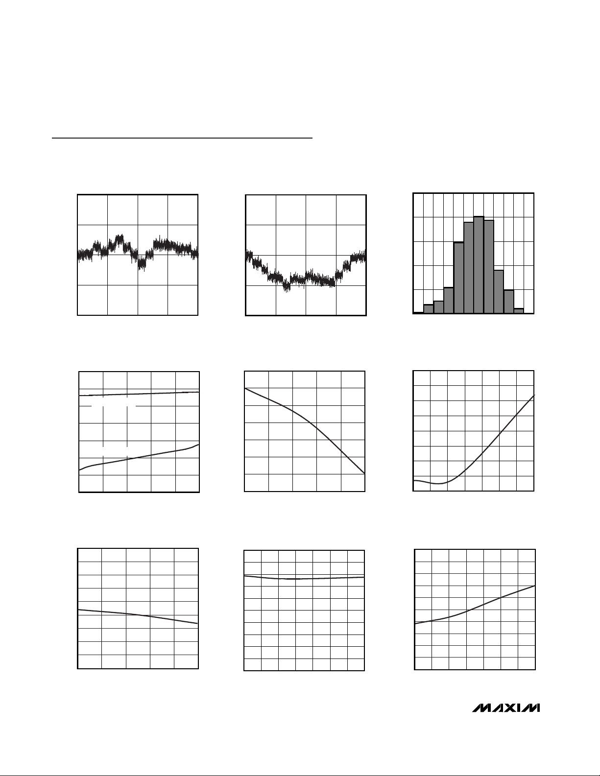
Typical Operating Characteristics
(AVDD= DVDD= 5V, GND = 0, external reference mode, REF+ = 2.048V, REF- = GND, RANGE bit = 1, internal clock mode, TA=
+25°C, unless otherwise noted.)
MAX1494
(±200mV INPUT RANGE) INL vs. OUTPUT CODE
MAX1492/94 toc01
OUTPUT CODE
INL (COUNTS)
10,0000-10,000
-0.5
0
0.5
1.0
-1.0
-20,000 20,000
MAX1494
(±2V INPUT RANGE) INL vs. OUTPUT CODE
MAX1492/94 toc02
OUTPUT CODE
INL (COUNTS)
10,0000-10,000
-0.5
0
0.5
1.0
-1.0
-20,000 20,000
NOISE DISTRIBUTION
MAX1492/94 toc03
NOISE (LSB)
PERCENTAGE OF UNITS (%)
0.80.70.60.50.40.30.20.10-0.1
5
10
15
20
25
0
-0.2
SUPPLY CURRENT
vs. SUPPLY VOLTAGE
MAX1492/94 toc04
SUPPLY VOLTAGE (V)
SUPPLY CURRENT (µA)
4.754.253.753.25
100
200
300
400
500
600
700
0
2.75 5.25
ANALOG SUPPLY
DIGITAL SUPPLY
MAX1494
OFFSET ERROR vs. SUPPLY VOLTAGE
MAX1492/94 toc05
SUPPLY VOLTAGE (V)
OFFSET ERROR (LSB)
4.754.253.753.25
-0.11
-0.06
-0.01
0.04
0.09
0.14
0.19
-0.16
2.75 5.25
MAX1494
OFFSET ERROR vs. TEMPERATURE
MAX1492/94 toc06
TEMPERATURE (°C)
OFFSET ERROR (LSB)
605010 20 30 40
-0.1
0
0.1
0.2
0.3
0.4
0.5
0.6
-0.2
070
MAX1494
GAIN ERROR vs. SUPPLY VOLTAGE
MAX1492/94 toc07
SUPPLY VOLTAGE (V)
GAIN ERROR (% FULL SCALE)
4.754.253.25 3.75
-0.08
-0.04
-0.06
-0.02
0
0.02
0.04
0.06
0.08
-0.10
2.75 5.25
MAX1494
GAIN ERROR vs. TEMPERATURE
MAX1492/94 toc08
TEMPERATURE (°C)
GAIN ERROR (% FULL SCALE)
605030 402010
-0.09
-0.08
-0.07
-0.06
-0.05
-0.04
-0.03
-0.02
-0.01
0
-0.10
070
INTERNAL REFERENCE VOLTAGE
vs. TEMPERATURE
MAX1492/94 toc09
TEMPERATURE (°C)
REFERENCE VOLTAGE (V)
605040302010
2.046
2.045
2.047
2.049
2.048
2.051
2.050
2.053
2.052
2.054
2.044
070
Page 7
MAX1492/MAX1494
3.5- and 4.5-Digit, Single-Chip ADCs
with LCD Drivers
_______________________________________________________________________________________ 7
INTERNAL REFERENCE VOLTAGE
vs. ANALOG SUPPLY VOLTAGE
MAX1492/94 toc10
SUPPLY VOLTAGE (V)
REFERENCE VOLTAGE (V)
4.754.253.753.25
2.045
2.046
2.047
2.048
2.049
2.050
2.044
2.75 5.25
SUPPLY CURRENT
vs. TEMPERATURE
MAX1492/94 toc11
TEMPERATURE (°C)
SUPPLY CURRENT (µA)
605040302010
100
200
300
400
500
600
700
0
070
ANALOG SUPPLY
DIGITAL SUPPLY
SHUTDOWN SUPPLY CURRENT
vs. TEMPERATURE
MAX1492/94 toc12
TEMPERATURE (°C)
SUPPLY CURRENT (µA)
605040302010
50
100
150
200
250
300
0
070
ANALOG SUPPLY
DIGITAL SUPPLY
SHUTDOWN SUPPLY CURRENT
vs. SUPPLY VOLTAGE
MAX1492/94 toc13
SUPPLY VOLTAGE (V)
SUPPLY CURRENT (µA)
4.754.253.753.25
50
100
150
200
250
300
0
2.75 5.25
ANALOG SUPPLY
DIGITAL SUPPLY
CHARGE-PUMP OUTPUT VOLTAGE
vs. ANALOG SUPPLY VOLTAGE
MAX1492/94 toc14
SUPPLY VOLTAGE (V)
V
NEG
VOLTAGE (V)
4.754.253.753.25
-2.48
-2.46
-2.44
-2.42
-2.40
-2.50
2.75 5.25
V
NEG
STARTUP SCOPE SHOT
MAX1492/94 toc15
20ms/div
2V/div
1V/div
V
DD
V
NEG
OFFSET ERROR
vs. COMMON-MODE VOLTAGE
MAX1492/94 toc16
COMMON-MODE VOLTAGE (V)
OFFSET ERROR (LSB)
1.51.0-1.5 -1.0 -0.5 0 0.5
-0.15
-0.10
-0.05
0
0.05
0.10
0.15
0.20
-0.20
-2.0 2.0
DATA OUTPUT RATE
vs. TEMPERATURE
MAX1492/94 toc17
TEMPERATURE (°C)
DATA OUTPUT RATE (Hz)
6035-15 10
4.92
4.98
4.96
4.94
5.00
5.02
5.04
5.06
5.08
5.10
4.90
-40 85
DATA OUTPUT RATE
vs. SUPPLY VOLTAGE
MAX1492/94 toc18
SUPPLY VOLTAGE (V)
DATA OUTPUT RATE (Hz)
4.744.233.21 3.72
4.995
4.990
4.985
5.000
5.005
5.010
5.015
5.020
4.980
2.70 5.25
Typical Operating Characteristics (continued)
(AVDD= DVDD= 5V, GND = 0, external reference mode, REF+ = 2.048V, REF- = GND, RANGE bit = 1, internal clock mode, TA=
+25°C, unless otherwise noted.)
Page 8
MAX1492/MAX1494
3.5- and 4.5-Digit, Single-Chip ADCs
with LCD Drivers
8 _______________________________________________________________________________________
Pin Description
PIN
MAX1492
NAME FUNCTION
130CLK
External Clock Input. When the EXTCLK bit in the control register is set, CLK is the
master clock input for the modulator and the filter (frequency = 4.9152MHz). When the
EXTCLK bit in the control register is reset, the internal clock is used. Connect CLK to
GND or DV
DD
when the internal oscillator is used.
231DV
DD
Digital Power Input. Connect DVDD to a 2.7V to 5.25V power supply. Bypass DVDD to
GND with 0.1µF and 4.7µF capacitors.
332GND Ground
41AV
DD
Analog Power Input. Connect AVDD to a 2.7V to 5.25V power supply. Bypass AVDD to
GND with 0.1µF and 4.7µF capacitors.
52AIN+
Positive Analog Input. Positive side of fully differential analog input. Bypass AIN+ to
GND with a 0.1µF or greater capacitor.
63AIN-
Negative Analog Input. Negative side of fully differential analog input. Bypass AIN- to
GND with a 0.1µF or greater capacitor.
74REF-
Negative Reference Input. During internal reference operation, connect REF- to GND.
For external reference operation, bypass REF- to GND with a 0.1µF capacitor and set
V
REF-
from -2.2V to +2.2V, provided V
REF+
> V
REF-
.
85REF+
Positive Reference Input. During internal reference operation, connect a 4.7µF capacitor
from REF+ to GND. For external reference operation, bypass REF+ to GND with a 0.1µF
capacitor and set V
REF+
from -2.2V to +2.2V, provided V
REF+
> V
REF-
.
96
Low-Battery Input. When V
LOWBATT
< 2.048V (typ), the LOWBATT symbol on LCD turns
on and the LOWBATT bit latches high in the status register.
10 7 EOC
Active-Low, End-of-Conversion Logic Output. A logic-low at EOC indicates that a new
ADC result is available in the ADC result register.
11 8 CS Active-Low Chip-Select Input. Forcing CS low activates the serial interface.
12 9 DIN
Serial Data Input. Data present at DIN is shifted into the internal registers in response to
a rising edge at SCLK when CS is low.
13 10 SCLK
Serial Clock Input. Apply an external clock to SCLK to facilitate communication through
the serial bus. SCLK can idle high or low.
14 11 DOUT
Serial Data Output. DOUT presents serial data in response to register queries. Data
shifts out on the falling edge of SCLK. DOUT goes high impedance when CS is high.
15 12 SEG1 LCD Segment 1 Driver
16 13 SEG2 LCD Segment 2 Driver
17 14 SEG3 LCD Segment 3 Driver
18 15 SEG4 LCD Segment 4 Driver
19 16 SEG5 LCD Segment 5 Driver
20 17 SEG6 LCD Segment 6 Driver
21 18 SEG7 LCD Segment 7 Driver
22 19 SEG8 LCD Segment 8 Driver
23 20 SEG9 LCD Segment 9 Driver
MAX1494
LOWBATT
Page 9
MAX1492/MAX1494
3.5- and 4.5-Digit, Single-Chip ADCs
with LCD Drivers
_______________________________________________________________________________________ 9
Pin Description (continued)
PIN
MAX1492
NAME
FUNCTION
24 21 SEG10 LCD Segment 10 Driver
25 25 BP3 LCD Backplane 3 Driver
26 26 BP2 LCD Backplane 2 Driver
27 27 BP1 LCD Backplane 1 Driver
28 29 V
NEG
-2.42V Charge-Pump Output. Bypass V
NEG
to GND with a 0.1µF capacitor.
—22SEG11 LCD Segment 11 Driver
—23SEG12 LCD Segment 12 Driver
—24SEG13 LCD Segment 13 Driver
—28V
DISP
Temperature-Compensation Voltage Input for LCD. If not using temperature
compensation, connect V
DISP
to GND. See the V
DISP
LCD Compensation section.
MAX1494
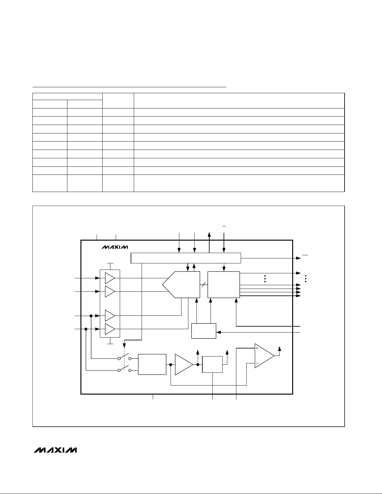
BINARY-TO-BCD
CONVERTERS
AND
LCD DRIVERS
ADC
INPUT
BUFFERS
-2.5V
AIN+
AIN-
REF+
REF-
+2.5V
AV
DD
DV
DD
V
DISP
2.048V
BANDGAP
REFERENCE
OSCILLATOR/
CLOCK
SCLK DIN DOUT
EOC
SEG1
SEG13
BP1
BP2
BP3
CLK
CS
SERIAL I/O AND CONTROL
+2.5V
GND
A = 1.22
TO
CONTROL
CHARGE
PUMP
-2.5V
LOWBATTV
NEG
Figure 1. MAX1494 Functional Diagram
MAX1494
Page 10
MAX1492/MAX1494
Detailed Description
The MAX1492/MAX1494 low-power, highly integrated
ADCs with LCD drivers convert a ±2V differential input
voltage (one count is equal to 100µV for the MAX1494
and 1mV for the MAX1492) with a sigma-delta ADC and
output the result to an LCD or µC. An additional
±200mV input range (one count is equal to 10µV for the
MAX1494 and 100µV for the MAX1492) is available to
measure small signals with increased resolution.
The devices operate from a single 2.7V to 5.25V power
supply and offer 3.5-digit (MAX1492) or 4.5-digit
(MAX1494) conversion results. An internal 2.048V reference, an internal charge pump, and a high-accuracy
on-chip oscillator eliminate external components.
The MAX1492 and MAX1494 interface with a µC using
an SPI/QSPI/MICROWIRE-compatible serial interface.
Data can either be sent directly to the display or to the
µC first for processing before being displayed.
The devices also feature on-chip buffers for the differential input signal and external reference inputs, allowing
direct interface with high-impedance signal sources. In
addition, they use continuous internal-offset calibration
and offer >100dB of 50Hz and 60Hz line noise rejection. Other features include data hold and peak hold,
overrange and underrange detection, and a low-battery
monitor.
Analog Input Protection
Internal protection diodes limit the analog input range
from V
NEG
to (AVDD+ 0.3V). If the analog input exceeds
this range, limit the input current to 10mA.
Internal Analog Input/Reference Buffers
The MAX1492/MAX1494 analog input/reference buffers
allow the use of high-impedance signal sources. The
input buffer’s common-mode input range allows the analog inputs and the reference to range from -2.2V to +2.2V.
Modulator
The MAX1492/MAX1494 perform analog-to-digital conversions using a single-bit, 3rd-order, sigma-delta modulator. The sigma-delta modulator converts the input
signal into a digital pulse train whose average duty
cycle represents the digitized signal information. The
modulator quantizes the input signal at a much higher
sample rate than the bandwidth of the input.
The MAX1492/MAX1494 modulator provides 3rd-order
frequency shaping of the quantization noise resulting
from the single-bit quantizer. The modulator is fully differential for maximum signal-to-noise ratio and minimum susceptibility to power-supply noise. A single-bit
data stream is then presented to the digital filter to
remove the frequency-shaped quantization noise.
Digital Filtering
The MAX1492/MAX1494 contain an on-chip digital lowpass filter that processes the data stream from the
modulator using a SINC4((sinx/x)4) response. The
SINC4filter has a settling time of four output data periods (4 x 200ms).
The MAX1492/MAX1494 have 25% overrange capability
built into the modulator and digital filter.
The digital filter is optimized for f
CLK
equal to 4.9152MHz.
Lower clock frequencies can be used; however,
50Hz/60Hz noise rejection decreases. The frequency
response of the SINC
4
filter is measured as follows:
where N is the oversampling ratio, and fm = N ✕ output
data rate = 5Hz.
Filter Characteristics
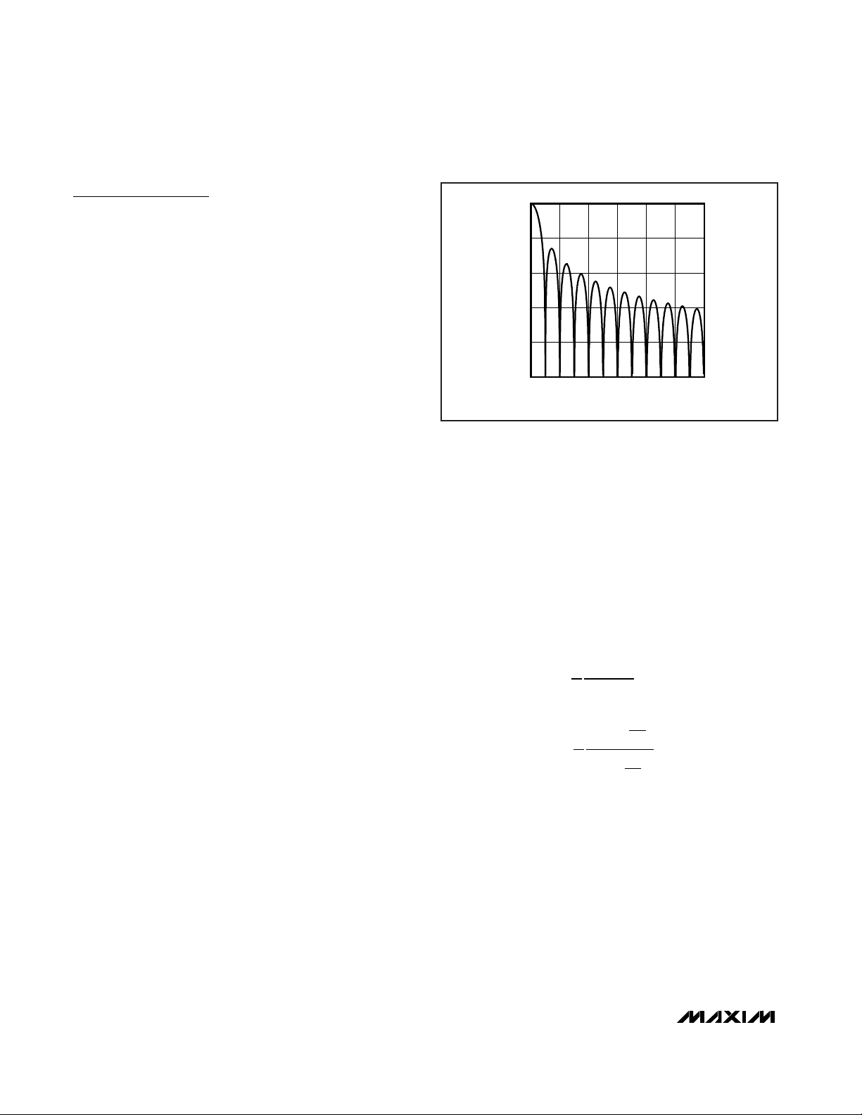
Figure 2 shows the filter frequency response. The
SINC4characteristic -3dB cutoff frequency is 0.228
times the first-notch frequency (5Hz).
The output data rate for the digital filter corresponds
with the positioning of the first notch of the filter’s frequency response. The notches of the SINC4filter are
repeated at multiples of the first-notch frequency. The
SINC4filter provides an attenuation of better than
100dB at these notches. For example, 50Hz is equal to
Hz
N
z
z
Hf
N
N
f
fm
f
fm
N
()
()
()
()
sin
sin
=
−
−
=
−
−
11
1
1
1
4
4
π
π
3.5- and 4.5-Digit, Single-Chip ADCs
with LCD Drivers
10 ___________________________________________________________________________________________________
FREQUENCY (Hz)
GAIN (dB)
5040302010
-160
-120
-80
-40
0
-200
060
Figure 2. Frequency Response of the SINC4Filter (Notch at 60Hz)
Page 11
ten times the first-notch frequency and 60Hz is equal to
12 times the first-notch frequency.
For large step changes at the input, allow a settling
time of 800ms before valid data is read.
Clock Modes
Configure the MAX1492/MAX1494 to use either the
internal oscillator or an externally applied clock to drive
the modulator and filter. Set the EXTCLK bit in the control register to 0 to put the device in internal clock mode.
Set the EXTCLK bit high to put the device in external
clock mode. Connect CLK to GND or DVDDwhen using
the internal oscillator. The MAX1492/MAX1494 ideally
operate with a 4.9152MHz clock to achieve maximum
rejection of 50Hz/60Hz common-mode, power-supply,
and normal-mode noise.
Internal Clock Mode
The MAX1492/MAX1494 contain an internal oscillator.
The power-up condition for the MAX1492/MAX1494 is
internal clock operation with the EXTCLK bit in the control register equal to 0. Using the internal oscillator
saves board space by removing the need for an external clock source.
External Clock Mode
For external clock operation, set the EXTCLK bit in the
control register high and drive CLK with a 4.9152MHz
clock source. Using an external clock allows for custom
conversion rates. A 2.4576MHz clock signal reduces
the conversion rate and the LCD update rate by a factor of two. The MAX1492/MAX1494 operate with an
external clock source of up to 5.05MHz.
Charge Pump
The MAX1492/MAX1494 contain an internal charge
pump to provide the negative supply voltage for the internal analog input/reference buffers. The bipolar input
range of the analog input/reference buffers allows this
device to accept negative inputs with high source impedances. Connect a 0.1µF capacitor from V
NEG
to GND.
LCD Driver
The MAX1492/MAX1494 contain the necessary backplane and segment-driver outputs to drive 3.5-digit
(MAX1492) and 4.5-digit (MAX1494) LCDs. The LCD
update rate is 2.5Hz. Figures 4–7 show the connection
schemes for a standard LCD. The MAX1492/MAX1494
automatically display the results of the ADC, if desired.
The MAX1492/MAX1494 also allow independent control
of the LCD driver through the serial interface, allowing
for data processing of the ADC result before showing
the result on the LCD. Additionally, each LCD segment
can be individually controlled (see the LCD Segment-
Display Register sections).
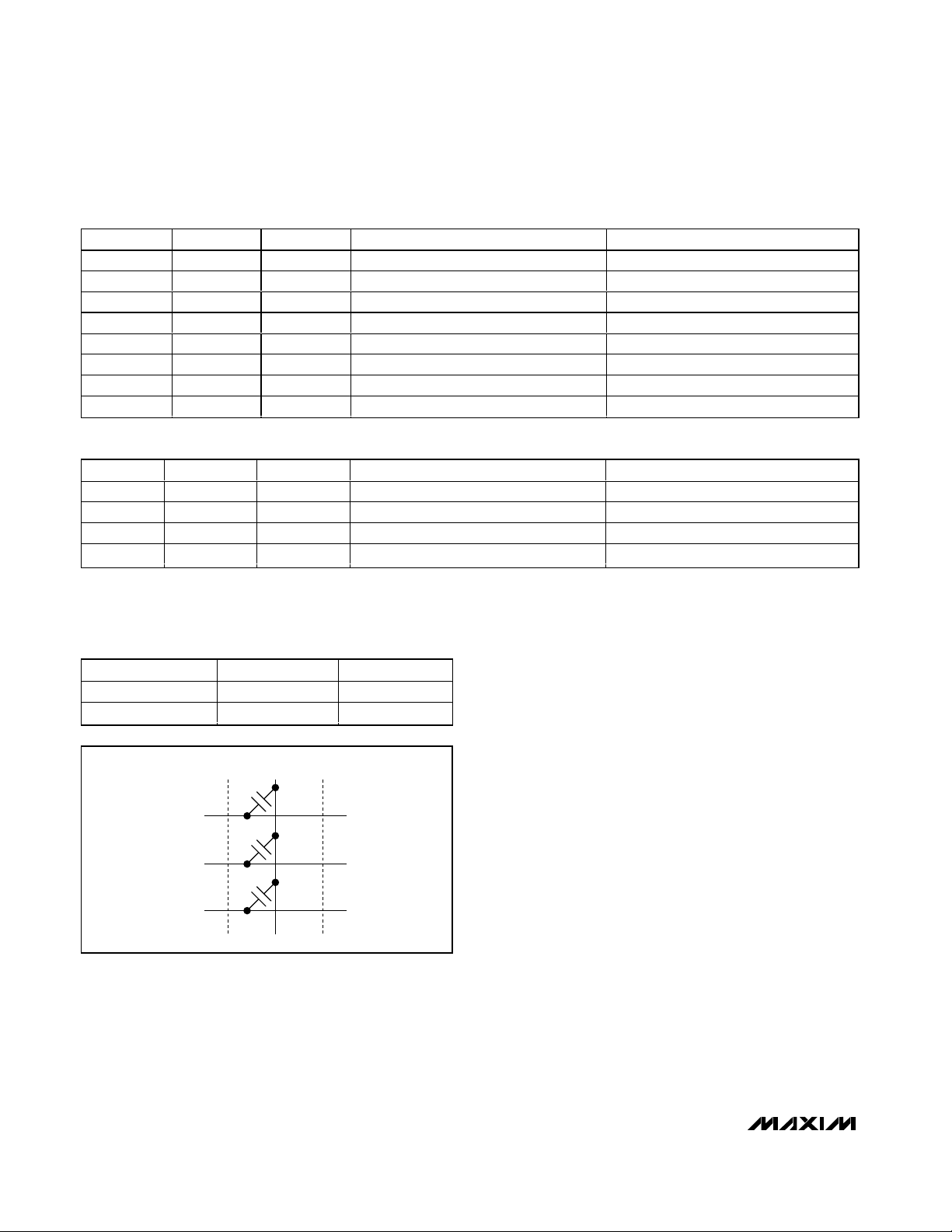
Triplexing
An internal resistor string comprised of three equalvalue resistors (52kΩ, 1% matching) is used to generate the display drive voltages. On the MAX1492, one
end of the string is connected to DVDDand the other
end is connected to GND. On the MAX1494, the other
end of the resistor string is connected to V
DISP
. Note
that V
LCD
should be three times the threshold voltage
for the liquid crystal material used (Figure 9).
The connection diagrams for a typical 7-segment display-font decimal point and annunciators are illustrated
in Figures 3 and 8. The MAX1494/MAX1492 numeric
display drivers (4.5 digits, 3.5 digits) use this configuration to drive a triplexed LCD with three backplanes and
13 segment-driver lines (10 for 3.5 digits). Figures 4
MAX1492/MAX1494
3.5- and 4.5-Digit, Single-Chip ADCs
with LCD Drivers
______________________________________________________________________________________ 11
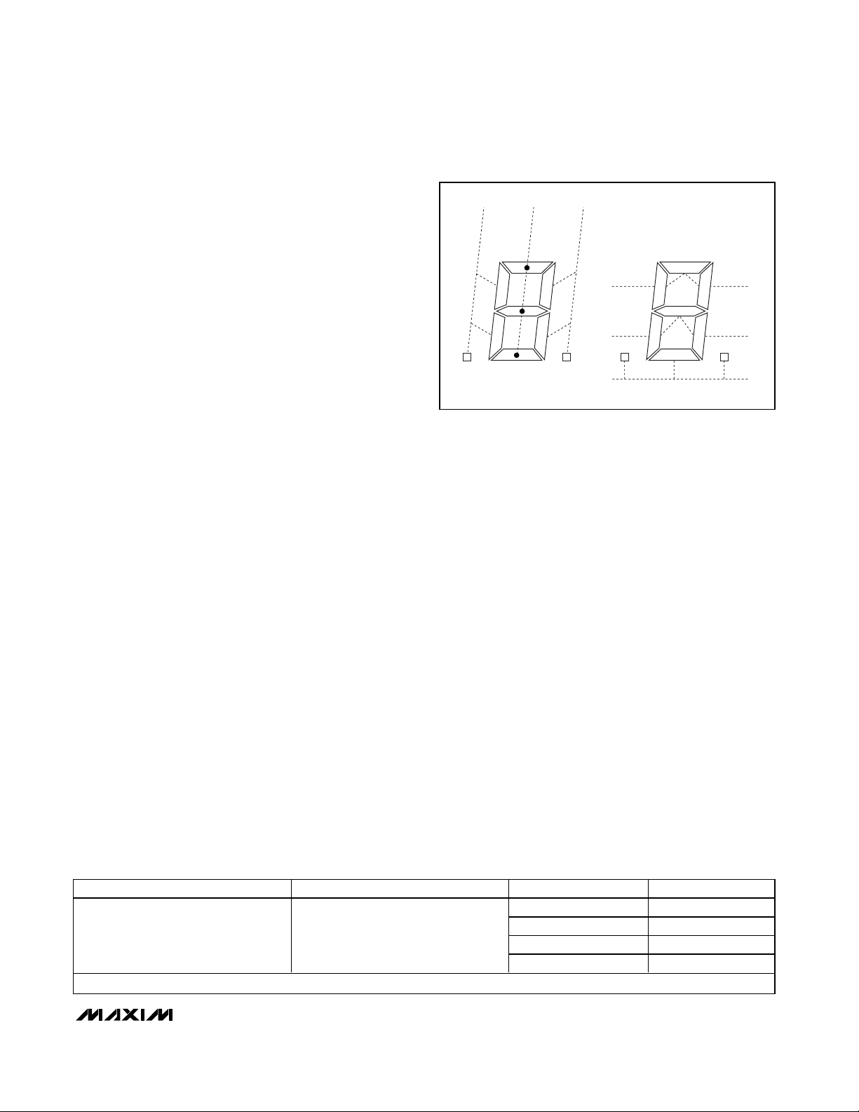
a
XYZ
g
d
e
f
c
b
DP
ANNUNCIATOR
a
g
d
e
f
c
b
DP ANNUNCIATOR
BP1
BP2
BP3
Figure 3. Connection Diagrams for Typical 7-Segment Displays
MANUFACTURER WEBSITE PART NUMBER DESCRIPTION
04-0924-00 3.5 digit, 5V
04-0924-01 3.5 digit, 3V
04-0925-00 4.5 digit, 5V
DCI, Inc. www.dciincorporated.com
04-0925-01 4.5 digit, 3V
The following site has links to other custom LCD manufacturers: www.earthlcd.com/mfr.htm
Table 1. List of Custom LCD Manufacturers
Page 12

MAX1492/MAX1494
and 5 show the assignment of the 4.5-digit display segments, and Figures 6 and 7 show the assignment of the
3.5-digit display segments.
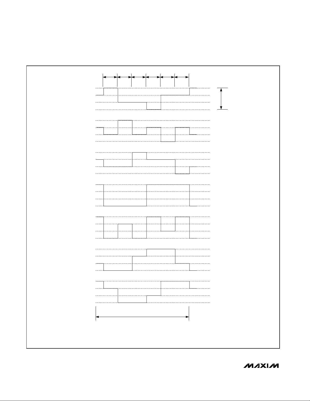
The voltage waveforms of the backplane lines and Y
segment line (Figure 3) have been chosen as an example. This line intersects with BP1 to form the a segment,
with BP2 to form the g segment, and with BP3 to form
the d segment. Eight different ON/OFF combinations of
the a, g, and d segments and their corresponding
waveforms of the Y segment line are illustrated in
Figures 9 and 10. The schematic diagram in Figure 8
shows each intersection as a capacitance from segment line to common line. Figure 11 illustrates the voltage across the g segment.
The RMS voltage across the segment determines the
degree of polarization for the liquid crystal material and
3.5- and 4.5-Digit, Single-Chip ADCs
with LCD Drivers
12 ______________________________________________________________________________________
HOLD LOW BATTPEAK
BP1
BP2
BP3
Figure 4. Backplane Connection for the MAX1494 (4.5 Digits)
HOLD
LOW BATT
PEAK
SEG13: PEAK, HOLD, N.C.
SEG2: A1, G1, D1
SEG12: F4, E4, DP4
SEG11: A4, G4, D4
SEG10: B4, C4, BC5
SEG9: F3, E3, DP3
SEG8: A3, G3, D3
SEG1: B1, C1, N.C.
SEG3: F1, E1, DP1
SEG4: B2, C2, LOWBATT
SEG5: A2, G2, D2
SEG6: F2, E2, DP2
SEG7: B3, C3, MINUS
ANNUNCIATOR
Figure 5. Segment Connection for the MAX1494 (4.5 Digits)
Page 13

thus the contrast of the segment. The RMS OFF voltage
is always V
LCD
/ 3, whereas the RMS ON voltage is
always 1.92V
LCD
/ 3. This is illustrated in Figure 11. The
ratio of RMS ON to RMS OFF voltage is fixed at 1.92 for
a triplexed LCD.
Figure 12 illustrates contrast vs. applied RMS voltage
with a V
LCD
of 3.1V. The RMS ON voltage is 2.1V, and
the RMS OFF voltage is 1.1V. The OFF segment has a
contrast of less than 5%, while the ON segments have
greater than 85% contrast.
If ghosting is present on the LCD, the RMS OFF voltage
is too high. Choose an LCD with a higher RMS OFF
voltage. Alternatively, lower the supply or apply a voltage on V
DISP
to lower the RMS OFF voltage.
Figures 9 and 10 show the voltage on the LCD’s BP_
inputs and the segment inputs during normal operation.
MAX1492/MAX1494
3.5- and 4.5-Digit, Single-Chip ADCs
with LCD Drivers
______________________________________________________________________________________ 13
HOLD
LOW BATT
PEAK
SEG10: PEAK, HOLD, BC4
SEG2: A1, G1, D1
SEG9: F3, E3, DP3
SEG8: A3, G3, D3
SEG1: B1, C1, N.C.
SEG3: F1, E1, DP1
SEG4: A2, G2, LOWBATT
SEG5: A2, G2, D2
SEG6: F2, E2, DP2
SEG7: B3, C3, MINUS
ANNUNCIATOR
Figure 7. Segment Connection for the MAX1492 (3.5 Digits)
HOLD LOW BATTPEAK
BP1
BP2
BP3
Figure 6. Backplane Connection for the MAX1492 (3.5 Digits)
Page 14
MAX1492/MAX1494
The MAX1492/MAX1494 allow for full decimal-point control and feature leading zero suppression. Use the
DP_EN, DPSET1, and DPSET2 bits in the control register
to set the value of the decimal point. Tables 2 and 3 show
the truth tables of the DP_EN, DPSET1, and DPSET2. The
truth tables determine decimal-point usage.
The MAX1492/MAX1494 overrange and underrange
display is shown in Table 4.
Reference
The MAX1492/MAX1494 reference sets the full-scale
range of the ADC transfer function. With a nominal
2.048V reference, the ADC full-scale range is ±2V with
the RANGE bit equal to 0. With the RANGE bit set to 1,
the full-scale range is ±200mV. A decreased reference
voltage decreases full-scale range (see the Transfer
Functions section).
The MAX1492/MAX1494 accept either an external reference or an internal reference. The INTREF bit selects
the reference mode (see the Control Register
(Read/Write) section).
For internal-reference operation, set INTREF to 1, connect REF- to GND and bypass REF+ to GND with a
4.7µF capacitor. The internal reference provides a nominal 2.048V source between REF+ and GND. The internal-reference temperature coefficient is typically
40ppm/°C.
The default power-on state sets the MAX1492/
MAX1494 to use the external reference with INTREF
cleared to 0. The external reference inputs, REF+ and
REF-, are fully differential. For a valid external-reference
input, V
REF+
must be greater than V
REF-
. Bypass REF+
and REF- with a 0.1µF or greater capacitor to GND in
external-reference mode.
3.5- and 4.5-Digit, Single-Chip ADCs
with LCD Drivers
14 ______________________________________________________________________________________
BP1
BP2
BP3
DP
DP
f
e
d
g
ab
c
XYZ
Figure 8. Schematic of Display Digit
DP_EN DPSET1 DPSET2 DISPLAY OUTPUT ZERO INPUT READING
000 1 8 8 8 8 0
001 1 8 8 8 8 0
010 1 8 8 8 8 0
011 1 8 8 8 8 0
100 1 8 8 8.8 0.0
1011 8 8.8 8 0.00
1101 8.8 8 8 0.000
111 1.8 8 8 8 0.0000
Table 2. Decimal-Point Control Table (MAX1494)
DP_EN DPSET1 DPSET2 DISPLAY OUTPUT ZERO INPUT READING
X0 0 1 8 8.8 0.0
X0 11 8.8 8 0.00
X1 0 1.8 8 8 0.000
X1 1 1 8 8 8 000
Table 3. Decimal-Point Control Table (MAX1492)
X = Don’t care.
CONDITION MAX1492 MAX1494
OVERRANGE 1– – – 1– – – –
UNDERRANGE -1– – – -1– – – –
Table 4. LCD During Overrange and
Underrange Conditions
Page 15

Figure 21 shows the MAX1492/MAX1494 operating with
an external single-ended reference. In this mode, REFis connected to GND and REF+ is driven with an external 2.048V reference. Bypass REF+ to GND with a
0.47µF capacitor.
Figure 20 shows the MAX1492/MAX1494 operating with
an external differential reference. In this mode, REFis connected to the top of the strain gauge and REF+
is connected to the midpoint of the resistor-divider of
the supply.
MAX1492/MAX1494
3.5- and 4.5-Digit, Single-Chip ADCs
with LCD Drivers
______________________________________________________________________________________ 15
φ1 φ2 φ3 φ1' φ2' φ3'
V+
V
H
V
L
V-
V+
V
H
V
L
V-
V+
V
H
V
L
V-
V+
V
H
V
L
V-
V+
V
H
V
L
V-
V+
V
H
V
L
V-
V+
V
H
V
L
V-
V
LCD
BP1
BP2
BP3
ALL
OFF
a ON
g, d OFF
g ON
a, d OFF
d ON
a, g OFF
FREQUENCY = 107Hz
φ1, φ2, φ3 - - BP HIGH WITH RESPECT TO SEGMENT (BP+ TIME)
φ1', φ2', φ3' - - BP LOW WITH RESPECT TO SEGMENT (BP- TIME)
BP1 ACTIVE DURING φ1 AND φ1'
BP2 ACTIVE DURING φ2 AND φ2'
BP3 ACTIVE DURING φ3 AND φ3'
V+ = DV
DD
, VH = 2/3 DV
DD
VL = 1/3 V
LCD
, V- = GND OR V
DISP
V
LCD
= D
VDD
- V
DISP
(MAX1494)
V
LCD
= D
VDD
- GND (MAX1492)
Figure 9. LCD Voltage Waveform—Combinations 1–4 (BP_, SEG2/5/8)
Page 16
MAX1492/MAX1494
3.5- and 4.5-Digit, Single-Chip ADCs
with LCD Drivers
16 ______________________________________________________________________________________
φ1 φ2 φ3 φ1' φ2' φ3'
V+
V
H
V
L
V-
V+
V
H
V
L
V-
V+
V
H
V
L
V-
V+
V
H
V
L
V-
V+
V
H
V
L
V-
V+
V
H
V
L
V-
V+
V
H
V
L
V-
V
LCD
BP1
BP2
BP3
ALL
OFF
a, d ON
g OFF
a, g ON
d OFF
g, d ON
a OFF
FREQUENCY = 107Hz
φ1, φ2, φ3 - - BP HIGH WITH RESPECT TO SEGMENT (BP+ TIME)
φ1', φ2', φ3' - - BP LOW WITH RESPECT TO SEGMENT (BP- TIME)
BP1 ACTIVE DURING φ1 AND φ1'
BP2 ACTIVE DURING φ2 AND φ2'
BP3 ACTIVE DURING φ3 AND φ3'
V+ = DV
DD
, VH = 2/3 DV
DD
VL = 1/3 V
LCD
, V- = GND OR V
DISP
V
LCD
= D
VDD
- V
DISP
(MAX1494)
V
LCD
= D
VDD
- GND (MAX1492)
Figure 10. LCD Voltage Waveform—Combinations 5–8 (BP_, SEG2/5/8)
Page 17

MAX1492/MAX1494
3.5- and 4.5-Digit, Single-Chip ADCs
with LCD Drivers
______________________________________________________________________________________ 17
φ1 φ2 φ3 φ1' φ2' φ3'
V
LCD
-V
P
0
V
RMS
= V
LCD
/ 3 OFF
V
P
-V
P
0
V
RMS
= V
LCD
/ 3 OFF
V
P
-V
P
0
V
RMS
= 1.92V
LCD
/ 3 ON
V
P
-V
P
0
V
RMS
= 1.92V
LCD
/ 3 ON
ALL
OFF
φ1, φ2, φ3 - - BP HIGH WITH RESPECT TO SEGMENT (BP+ TIME)
φ1', φ2', φ3' - - BP LOW WITH RESPECT TO SEGMENT (BP- TIME)
BP1 ACTIVE DURING φ1 AND φ1'
BP2 ACTIVE DURING φ2 AND φ2'
BP3 ACTIVE DURING φ3 AND φ3'
V
G
= VY - V
BP2
(DIFFERENCE BETWEEN SEGMENT LINE Y AND BP2 VOLTAGE)
VOLTAGE CONTRAST RATIO = V
RMS
ON / V
RMSOFF
= 1.922V
a ON
g, d OFF
a, g ON
d OFF
ALL
ON
Figure 11. Voltage Waveforms on the g Segment
Page 18

MAX1492/MAX1494
3.5- and 4.5-Digit, Single-Chip ADCs
with LCD Drivers
18 ______________________________________________________________________________________
012345
APPLIED VOLTAGE (V
RMS
)
0
10
20
30
40
50
60
70
80
90
100
CONTRAST (%)
TA = +25°C
V
ON
= 2.1V
RMS
Ø = -10°C
Ø = 0°C
Ø = +10°C
Ø = -30°C
V
OFF
=
1.1V
RMS
Ø+
Ø-
Figure 12. Contrast vs. Applied RMS Voltage
Page 19

MAX1492/MAX1494
3.5- and 4.5-Digit, Single-Chip ADCs
with LCD Drivers
______________________________________________________________________________________ 19
CS
SCLK
DIN
DOUT
t
CSH
t
CL
t
DS
t
DH
t
DV
t
CH
t
DO
t
TR
t
CSH
t
CSS
Figure 13. Detailed Timing Diagram
SCLK
CS
DIN
DOUT
10RS4 RS3 RS2 RS1 D7 D6 D5 D4 D3 D2 D1 D0D8D9RS0 x D15 D14 D13 D12 D11 D10
CONTROL BYTE DATA BYTE
Figure 14. Serial-Interface 16-Bit Write Timing Diagram
CS
SCLK
DIN
DOUT
10RS4 RS3 RS2 RS1 D7 D6 D5 D4 D3 D2 D1 D0RS0 x
CONTROL BYTE
DATA BYTE
Figure 15. Serial-Interface 8-Bit Write Timing Diagram
Page 20

MAX1492/MAX1494
3.5- and 4.5-Digit, Single-Chip ADCs
with LCD Drivers
20 ______________________________________________________________________________________
SCLK
CS
DIN
DOUT
11A4A3 A2 A1 A0 x
D7 D6 D5 D4 D3 D2 D1 D0
CONTROL BYTE
DATA BYTE
Figure 17. Serial-Interface 8-Bit Read Timing Diagram
6kΩ
6kΩ
DOUT
DOUT
GND
GND
DV
DD
C
LOAD
50pF
C
LOAD
50pF
A) VOH TO HIGH-Z B) VOL TO HIGH-Z
Figure 18. Load Circuits for Disable Time
6kΩ
6kΩ
DOUT
DOUT
GND
GND
DV
DD
C
LOAD
50pF
C
LOAD
50pF
B) HIGH-Z TO VOH AND VOL TO V
OH
B) HIGH-Z TO VOL AND VOH TO V
OL
Figure 19. Load Circuits for Enable Time
SCLK
CS
DIN
DOUT
11RS4 RS3 RS2 RS1 RS0 x
D7 D6 D5 D4 D3 D2 D1 D0D8D9D15 D14 D13 D12 D11 D10
CONTROL BYTE
DATA BYTE
Figure 16. Serial-Interface 16-Bit Read Timing Diagram
Page 21

MAX1492/MAX1494
3.5- and 4.5-Digit, Single-Chip ADCs
with LCD Drivers
______________________________________________________________________________________ 21
Applications Information
Serial Interface
The SPI/QSPI/MICROWIRE serial interface consists of a
chip select (CS), a serial clock (SCLK), a data in (DIN),
a data out (DOUT), and an asynchronous EOC output.
EOC provides an asynchronous end-of-conversion signal with a period of 200ms (f
CLK
= 4.9152MHz or inter-
nal clock mode). The MAX1492 updates the data
register when EOC goes high. Data is valid in the ADC
result registers when EOC returns low. The serial interface provides access to 12 on-chip registers, allowing
control to all the power modes and functional blocks.
Table 5 lists the address and read/write accessibility of
all the registers.
A logic-high on CS tri-states DOUT and causes the
MAX1492/MAX1494 to ignore any signals on SCLK and
DIN. To clock data into or out of the internal shift register, drive CS low. SCLK synchronizes the data transfer.
The rising edge of SCLK clocks DIN into the shift register, and the falling edge of SCLK clocks DOUT out of
the shift register. DIN and DOUT are transferred MSBfirst (data is left justified). Figures 13–17 show the
detailed serial-interface timing diagrams for the 8- and
16-bit read/write operations.
All communication with the MAX1492/MAX1494 begins
with a command byte on DIN, where the first logic 1 on
DIN is recognized as the START bit (MSB) for the command byte. The following seven clock cycles load the
command into a shift register. These 7 bits specify
which of the registers are accessed next, and whether a
read or write operation takes place. Transitions on the
serial clock after the command byte transfer cause a
write or read from the device until the correct number of
bits have been transferred (8 or 16). Once this has
occurred, the MAX1492/MAX1494 wait for the next command byte. CS must not go high between data transfers. If CS is toggled before the end of a write or read
operation, the device mode may be unknown. Clock in
32 zeros to clear the device state and reset the interface
so it is ready to receive a new command byte.
On-Chip Registers
The MAX1492/MAX1494 contain 12 on-chip registers.
These registers configure the various functions of the
device and allow independent reading of the ADC
results and writing to the LCD. Table 5 lists the address
and size of each register.
The first of these registers is the status register. The 8-bit
status register contains the status flags for the ADC. The
second register is the 16-bit control register. This register
sets the LCD controls, range modes, power-down
modes, offset calibration, and the reset-register function
(CLR). The third register is the 16-bit overrange register,
which sets the overrange limit of the analog input. The
fourth register is the 16-bit underrange register, which
sets the underrange limit of the analog input. Registers 5
through 7 contain the display data for the individual segments of the LCD. The eighth register contains the custom offset value. The ninth register contains the 16 MSBs
of the ADC conversion result. The tenth register contains
the LCD data. The eleventh register contains the peak
analog input value. The last register contains the lower 4
LSBs of the 20-bit ADC conversion result.
REGISTER
NUMBER
ADDRESS
RS [4:0]
NAME WIDTH ACCESS
1 00000 Status Register 8 Read only
2 00001 Control Register 16 R/W
3 00010 Overrange Register 16 R/W
4 00011 Underrange Register 16 R/W
5 00100 LCD Segment-Display Register 1 16 R/W
6 00101 LCD Segment-Display Register 2 16 R/W
7 00110 LCD Segment-Display Register 3 8 R/W
8 00111 ADC Custom-Offset Register 16 R/W
9 01000 ADC Result-Register 1 (16 MSBs) 16 Read only
10 01001 LCD Data Register 16 R/W
11 01010 Peak Register 16 Read only
12 10100 ADC Result-Register 2 (4 LSBs) 8 Read only
— All Other Addresses Reserved — —
Table 5. Register Address Table
Page 22

MAX1492/MAX1494
3.5- and 4.5-Digit, Single-Chip ADCs
with LCD Drivers
22 ______________________________________________________________________________________
START: Start Bit. The first 1 clocked into the
MAX1492/MAX1494 is the first bit of the
command byte.
(R/W): Read/Write. Set this bit to 1 to read from
the specified register. Set this bit to 0 to
write to the selected register. Note that
certain registers are read-only. Write commands to a read-only register are
ignored.
(RS4–RS0): Register Address Bits. RS4 to RS0 specify
which register is accessed.
X: Don’t care.
MSB
LSB
Bit 7 Bit 6 Bit 5 Bit 4 Bit 3 Bit 2 Bit 1 Bit 0
START (1) R/W RS4 RS3 RS2 RS1 RS0 X
This register contains the status of the conversion
results.
SIGN: Latched Negative-Polarity Indicator.
Latches high when the result is negative.
Clears by reading the status register,
unless the condition remains true.
OVER: Overrange Bit. Latches high if an over-
range condition occurs (the ADC result is
larger than the value in the overrange register). Clears by reading the status register, unless the condition remains true.
UNDER: Underrange Bit. Latches high if an under-
range condition occurs (the ADC result is
less than the value in the underrange register). Clears by reading the status register,
unless the condition remains true.
LOW_BATT: Low-Battery Bit. Latches high if the voltage
at the LOWBATT is lower than 2.048V (typ).
Clears by reading the status register,
unless the condition remains true.
DRDY: Data-Ready Bit. Latches high to indicate
a completed conversion result with valid
data. Read the ADC Result-Register 1 to
clear this bit.
MSB
LSB
SIGN OVER UNDER LOW_BATT DRDY 0 0 0
This register is the primary control register for the
MAX1492/MAX1494. It is a 16-bit read/write register. It
is used to indicate the desired clock and reference
source. It sets the LCD controls, range modes, powerdown modes, offset calibration, and the reset register
function (CLR).
MSB
Bit 15 Bit 14 Bit 13 Bit 12 Bit 11 Bit 10 Bit 9 Bit 8
SPI/ADC EXTCLK INTREF DP_EN DPSET2 DPSET1 PD_DIG PD_ANA
LSB
Bit 7 Bit 6 Bit 5 Bit 4 Bit 3 Bit 2 Bit 1 Bit 0
HOLD PEAK RANGE CLR SEG_SEL
0
Status Register (Read Only):
Control Register (Read/Write):
Command Byte (Write Only):
Default values: 0000h
Default values: 00h
OFFSET_CAL1 OFFSET_CAL2
Page 23

MAX1492/MAX1494
3.5- and 4.5-Digit, Single-Chip ADCs
with LCD Drivers
______________________________________________________________________________________ 23
SPI/ADC: (Default = 0) Display Select Bit. The
SPI/ADC bit controls selection of the
data fed into the LCD data register. A
1 in this location selects SPI/QSPI/
MICROWIRE data (the user writes this
data to the LCD data register). A 0 in
this location selects the ADC result
register data, unless hold or peak
functions are active (see Table 6).
EXTCLK: (Default = 0) External Clock Select
Bit. The EXTCLK bit controls selection of the internal clock or an external clock source. A 1 in this location
selects the signal at the CLK input as
the clock source. A 0 in this location
selects the internal clock oscillator.
Toggle the PD_DIG and PD_ANA
after changing the EXTCLK bit.
INTREF: (Default = 0) Reference Select Bit. For
internal reference operation, set
INTREF to 1. For external reference
operation, set INTREF to 0.
DP_EN: (Default = 0) Decimal-Point Enable
Bit. See Tables 2 and 3.
DPSET[2:1]: (Default = 00) Decimal-Point
Selection Bits. See Tables 2 and 3.
HOLD: (Default = 0) Hold Bit. When set to 1,
the LCD register does not update
from the ADC conversion results and
holds the last result on the LCD. The
MAX1492/MAX1494 continue to perform conversions during HOLD (see
Table 6).
PEAK: (Default = 0) Peak Bit. When set to 1
(and the HOLD bit is set to 0), the
LCD shows the result stored in the
peak register (see Table 6).
PD_ANA: (Default = 0) Power-Down Analog
Select Bit. When set to 1, the analog
circuits (analog modulator and ADC
input buffers) go into the power-down
mode. When set to 0, the device is in
full power-up mode.
PD_DIG: (Default = 0) Power-Down Digital
Select Bit. When set to 1, the digital
circuits (digital filter and LCD drivers)
go into power-down mode. This also
resets the values of the internal
SRAM (in the digital filter) to zeros.
When set to 0, the device returns to
full power-up mode.
RANGE: (Default = 0) Input-Range Select Bit.
When set to 0, the input voltage
range is ±2V. When set to 1, the input
voltage range is ±200mV. Toggle the
PD_DIG and PD_ANA after changing
the RANGE bit.
CLR: (Default = 0) Clear-All-Registers Bit.
When set to 1, all the registers reset
to their power-on reset states when
CS makes a low-to-high transition.
SEG_SEL: (Default = 0) LCD Segment-Selection
Bit. When set to 1, the LCD segment
drivers use the LCD segment registers to display individual segments
that can form letters or numbers or
other information on the display. The
LCD data register is NOT displayed.
Send the data first to the LCD segment-display registers and then set
this bit high (see Table 6).
OFFSET_CAL1: (Default = 0) Automatic-Offset Enable
Bit. When set to 1, the MAX1492/
MAX1494 disable automatic offset calibration. When this bit is set to 0, automatic offset calibration is enabled.
OFFSET_CAL2: (Default = 0) Enhanced Offset-
Calibration Start Bit (MAX1494 Only
and RANGE = 1). To achieve the lowest possible offset in the ±200mV
input range, perform an enhanced
offset calibration by setting this bit to
1. The calibration takes about 9
cycles (1800ms). After the calibration
completes, set this bit to 0 to resume
ADC conversions.
Note: When changing any one of the following control
bits: OFFSET_CAL1, RANGE, PD_ANA, PD_DIG,
INTREF, and EXTCLK, wait 800ms before reading the
ADC results.
Page 24

MAX1492/MAX1494
3.5- and 4.5-Digit, Single-Chip ADCs
with LCD Drivers
24 ______________________________________________________________________________________
Default values: 7CF0h (for MAX1492, +1999)
4E1Fh (for MAX1494, +19,999)
The overrange register is a 16-bit read/write register
(D15 is the MSB). When the conversion result exceeds
the value in the overrange register, the OVER bit in the
status register latches to 1. The LCD shows a 1 fol-
lowed by 4 dashes for the MAX1494 or a 1 followed by
3 dashes for the MAX1492 (see Table 4).
The data is represented in two’s complement format.
SEG_SEL SPI/ADC HOLD PEAK DISPLAYS VALUES FROM
1XXXLCD Segment Registers
01XXLCD Display Register (User Written)
001XLCD Display Register
0001Peak Register
0000ADC Result Register
Table 6. LCD Priority Table
X = Don’t care.
Underrange Register (Read/Write):
Overrange Register (Read/Write):
MSB
LSB
D15
D0
Default values: 8300h (for MAX1492, -2000)
B1E0h (for MAX1494, -20,000)
The underrange data register is 16-bit read/write register (D15 is the MSB). When the conversion result falls
below the value in the underrange register, the UNDR
bit in the status register sets to 1. The LCD shows a -1
followed by 4 dashes for the MAX1494 or a -1 followed
by 3 dashes for the MAX1492 (see Table 4).
The data is represented in two’s complement format.
MSB
LSB
D15
D0
Default values: 0000h
The LCD segment-display register 1 is a 16-bit
read/write register. When the SEG_SEL bit (in the control register) is set to 1, the MAX1492/MAX1494 provide
direct access to individual LCD segments. The bits in
the LCD segment-display register determine if a segment is on or off. Write a 0 to this register to turn on a
segment and a 1 to turn off a segment.
MSB
LSB
A2
F2 E2
F1 E1
0
LCD Segment-Display Register 1 (Read/Write):
D14 D13 D12 D11 D10 D9 D8 D7 D6 D5 D4 D3 D2 D1
D14 D13 D12 D11 D10 D9 D8 D7 D6 D5 D4 D3 D2 D1
G2 D2
DP2 ANN B1 C1 A1 G1 D1
DP1
Page 25

MAX1492/MAX1494
3.5- and 4.5-Digit, Single-Chip ADCs
with LCD Drivers
______________________________________________________________________________________ 25
Default values: 0000h
The LCD segment-display register 2 is a 16-bit
read/write register. When the SEG_SEL bit (in the control register) is set to 1, the MAX1492/MAX1494 provide
direct access to individual LCD segments. The bits in
the LCD segment-display register determine if a segment is on or off. Write a 0 to this register to turn on a
segment and a 1 to turn off a segment.
DP1: Segment DP Driver Bit of Digit 1. The
default value turns on the LCD segment.
E1: Segment e Driver Bit of Digit 1. The
default value turns on the LCD segment.
F1: Segment f Driver Bit of Digit 1. The
default value turns on the LCD segment.
D1: Segment d Driver Bit of Digit 1. The
default value turns on the LCD segment.
G1: Segment g Driver Bit of Digit 1. The
default value turns on the LCD segment.
A1: Segment a Driver Bit of Digit 1. The
default value turns on the LCD segment.
C1: Segment c Driver Bit of Digit 1. The
default value turns on the LCD segment.
B1: Segment b Driver Bit of Digit 1. The
default value turns on the LCD segment.
ANN: Custom Annunciator. The default value
turns on the LCD segment.
DP2: Segment DP Driver Bit of Digit 2. The
default value turns on the LCD segment.
E2: Segment e Driver Bit of Digit 2. The
default value turns on the LCD segment.
F2: Segment f Driver Bit of Digit 2. The
default value turns on the LCD segment.
D2: Segment d Driver Bit of Digit 2. The
default value turns on the LCD segment.
G2: Segment g Driver Bit of Digit 2. The
default value turns on the LCD segment.
A2: Segment a Driver Bit of Digit 2. The
default value turns on the LCD segment.
MSB
LSB
F4 E4
LOW
0
C2: Segment c Driver Bit of Digit 2. The
default value turns on the LCD segment.
B2: Segment b Driver Bit of Digit 2. The
default value turns on the LCD segment.
LOWBATT: LOWBATT Driver Bit. The default value
turns on the LOWBATT annunciator.
DP3: Segment DP Driver Bit of Digit 3. The
default value turns on the LCD segment.
E3: Segment e Driver Bit of Digit 3. The
default value turns on the LCD segment.
F3: Segment f Driver Bit of Digit 3. The
default value turns on the LCD segment.
D3: Segment d Driver Bit of Digit 3. The
default value turns on the LCD segment.
G3: Segment g Driver Bit of Digit 3. The
default value turns on the LCD segment.
A3: Segment a Driver Bit of Digit 3. The
default value turns on the LCD segment.
C3: Segment c Driver Bit of Digit 3. The
default value turns on the LCD segment.
B3: Segment b Driver Bit of Digit 3. The
default value turns on the LCD segment.
MINUS: Minus-Sign Driver Bit. The default value
turns on the LCD segment.
DP4: Segment DP Driver Bit of Digit 4. The
default value turns on the LCD segment
(MAX1494 only).
E4: Segment e Driver Bit of Digit 4. The
default value turns on the LCD segment
(MAX1494 only).
F4: Segment f Driver Bit of Digit 4. The
default value turns on the LCD segment
(MAX1494 only).
LCD Segment-Display Register 2 (Read/Write):
DP4 MINUS B3 C3 A3 G3 D3 F3 E3 DP3
BATT
B2 C2
Page 26

MAX1492/MAX1494
3.5- and 4.5-Digit, Single-Chip ADCs
with LCD Drivers
26 ______________________________________________________________________________________
Default values: 00h
The LCD segment-display register 3 is an 8-bit
read/write register. When the SEG_SEL bit (in the control register) is set to 1, the MAX1492/MAX1494 provide
direct access to individual LCD segments. The bits in
the LCD segment-display register determine if a segment is on or off. Write a 0 to turn on a segment and a 1
to turn off a segment.
MSB
LSB
PEAK HOLD BC_ B4 C4 A4 G4 D4
D4: Segment d Driver Bit of Digit 4. The
default value turns on the LCD segment
(MAX1494 only).
G4: Segment g Driver Bit of Digit 4. The
default value turns on the LCD segment
(MAX1494 only).
A4: Segment a Driver Bit of Digit 4. The
default value turns on the LCD segment
(MAX1494 only).
C4: Segment c Driver Bit of Digit 4. The
default value turns on the LCD segment
(MAX1494 only).
B4: Segment b Driver Bit of Digit 4. The
default value turns on the LCD segment
(MAX1494 only).
BC_: Segment bc_ Driver Bit. For the
MAX1494, this bit enables BC5. For the
MAX1492, this bit enables BC4. The
default value turns on the LCD segment.
HOLD: HOLD-Sign Driver Bit. The default value
turns on the HOLD annunciator.
PEAK: PEAK-Sign Driver Bit. The default value
turns on the PEAK annunciator.
Default values: 0000h
In addition to automatic offset calibration, the
MAX1492/MAX1494 offer a user-defined custom-offset
16-bit read/write register. The final result of the ADC
conversion is the input after autocalibration minus the
value in the custom offset. The custom offset value is
stored in this register. D15 is the MSB. The data is represented in two’s complement format.
MSB
LSB
D15
D0
Default values: 0000h
The ADC result-register 1 is a 16-bit read-only register.
This register stores the 16 MSBs of the ADC result. The
data is represented in two’s complement format.
For the MAX1494, the data is 16-bit and D15 is the
MSB. For the MAX1492, the data is 12-bit, D15 is the
MSB, and D4 is the LSB.
MSB
LSB
(MAX1492)
LSB
(MAX1494)
D15
D0
LCD Segment-Display Register 3 (Read/Write):
ADC Custom Offset-Calibration Register (Read/Write):
ADC Result-Register 1 (Read Only):
D14 D13 D12 D11 D10 D9 D8 D7 D6 D5 D4 D3 D2 D1
D14 D13 D12 D11 D10 D9 D8 D7 D6 D5 D4 D3 D2 D1
Page 27

MAX1492/MAX1494
3.5- and 4.5-Digit, Single-Chip ADCs
with LCD Drivers
______________________________________________________________________________________ 27
Default values: 0000h
The peak data register is a 16-bit read-only register.
Set the PEAK bit to 1 to enable the PEAK function. This
register stores the peak value of the ADC conversion
result. First, the current ADC result is saved to the
PEAK register. Then, the new ADC conversion result is
compared to this value. If the new value is larger than
the value in the peak register, the MAX1492/MAX1494
save the new value to the peak register. If the new
value is less than the value in the peak register,
the value in the peak register remains unchanged. Set
the PEAK bit to 0 to clear the value in the PEAK register. The peak function is only valid for the range of
-19,487 to +19,999 for the MAX1494 and -1217 to
+1999 for the MAX1492.
The data is represented in two’s complement format.
For the MAX1494, the data is 16-bit and D15 is the MSB.
For the MAX1492, the data is 12-bit, D15 is the MSB, and
D4 is the LSB followed by four trailing sub-bits.
Default values: 0000h
The LCD data register is a 16-bit read/write register.
This register updates from the ADC result register 1, the
PEAK register, or from the serial interface by selecting
SPI/ADC bit, PEAK bit, and HOLD bit in the control register (see Table 6). The data is represented in two’s
complement format.
For the MAX1494, the data is 16-bit and D15 is the MSB.
For the MAX1492, the data is 12-bit, D15 is the MSB,
and D4 is the LSB, followed by four trailing sub-bits.
MSB
LSB
(MAX1492)
LSB
(MAX1494)
D15
D0
Default values: 00h
The ADC result-register 2 is an 8-bit read-only register.
This register stores the 4 LSBs of the ADC result. Use
this result with the result in ADC result-register 1 to form
a 20-bit two’s complement conversion result.
LCD Data Register (Read/Write):
PEAK Register (Read Only):
ADC Result-Register 2 (Read Only):
D14 D13 D12 D11 D10 D9 D8 D7 D6 D5 D4 D3 D2 D1
MSB
D15 D14 D13 D12 D11 D10 D9 D8 D7 D6 D5 D4 D3 D2 D1 D0
LSB
(MAX1492)
LSB
(MAX1494)
MSB LSB
D3 D2 D1 D0 0000
Page 28

MAX1492/MAX1494
3.5- and 4.5-Digit, Single-Chip ADCs
with LCD Drivers
28 ______________________________________________________________________________________
Power-On Reset
At power-up, the serial interface, LCD driver, digital filter, and modulator circuits reset. The registers return to
their default values. Allow time for the reference to settle before starting calibration.
Offset Calibration
The MAX1492/MAX1494 offer on-chip offset calibration.
The device offset-calibrates during every conversion
when the OFFSET_CAL1 bit is 0. Enhanced offset calibration is only needed in the MAX1494 when RANGE = 1.
It is performed on demand by setting the OFFSET_CAL2
bit to 1.
Power-Down Modes
The MAX1492/MAX1494 feature independent powerdown control of the analog and digital circuitry. Writing a
1 to the PD_DIG and PD_ANA bits in the control register
powers down the analog and digital circuitry, reducing
the supply current to 400µA. PD_DIG powers down the
digital filter and LCD drivers, while PD_ANA powers
down the analog modulator and ADC input buffers.
V
DISP
LCD Compensation (MAX1494 Only)
Adequate display contrast can be obtained in most
applications by connecting V
DISP
to GND. In applications where a wide temperature range is expected, the
voltage levels for some triplexed LCDs may need to vary
with temperature to maintain good display contrast and
viewing angle. The amount of temperature compensation depends upon the type of liquid crystal used.
Display manufacturers usually specify the temperature
variation of the LCD thresholds voltage (RMSONRMS
OFF
), which is approximately 1/3 of the peak dis-
play voltage. The peak display voltage is equal to DV
DD
- V
DISP
(MAX1494 only). Therefore, a typical -4mV/°C
temperature coefficient of an LCD threshold corresponds to a +12mV/°C temperature coefficient at V
DISP
.
Peak
The MAX1492/MAX1494 feature peak-detection circuitry. When activated (PEAK bit = 1), the devices display
only the highest voltage measured to the LCD.
Hold
The MAX1492/MAX1494 feature data-hold circuitry.
When activated (HOLD bit = 1), the devices display the
current reading on the LCD.
Low Battery
The MAX1492/MAX1494 feature a low-battery detection
input. When the voltage at LOWBATT drops below
2.048V (typ), the LOWBATT bit of the status register goes
high and the LOWBATT segment of the LCD turns on.
Strain Gauge Measurement
Connect the differential inputs of the MAX1492/
MAX1494 to the bridge network of the strain gauge. In
Figure 20, the analog supply voltage powers the bridge
network and the MAX1492/MAX1494 along with the reference voltage. The MAX1492/MAX1494 handle an
analog input-voltage range of ±200mV and ±2V full
scale. The analog/reference inputs of the parts allow
the analog input range to have an absolute value of
anywhere between -2.2V and +2.2V.
Thermocouple Measurement
Figure 21 shows a connection from a thermocouple to
the MAX1492/MAX1494. In this application, the
MAX1492/MAX1494 take advantage of the on-chip input
buffers that allow large source impedances on the front
end. The decoupling capacitors reduce noise pickup
from the thermocouple leads. To place the differential
voltage from the thermocouple at a suitable commonmode voltage, the AIN- input of the MAX1492/MAX1494
is biased to GND. Use an external temperature sensor,
such as the DS75, and a µC to perform cold junctiontemperature compensation.
4–20mA Transmitter
Low-power, single-supply operations make the
MAX1492/MAX1494 ideal for loop-powered 4–20mA
transmitters. Loop-powered transmitters draw their
power from the 4–20mA loop, limiting the transmitter
circuitry to a current budget of 4mA. Tolerances in the
loop further limit this current budget to 3.5mA. Since
the MAX1492/MAX1494 only consume 950µA, a total of
2.55mA remains to power the remaining transmitter circuitry. Figure 22 shows a block diagram for a looppowered 4–20mA transmitter.
4–20mA Measurement
To measure 4–20mA signals, connect a shunt resistor
across AIN+ and AIN- to create the ±2V or ±200mV
input voltage (Figure 23).
Transfer Functions
Figures 24–27 show the transfer functions of the
MAX1492/MAX1494. The output data is stored in the
ADC data register in two’s complement.
A -1 in the ADC result register displays -0 on the LCD as
shown in Figures 24–27. Negative values on the LCD
are offset by 1. For example, -100 in the ADC result register appears as -99 on the LCD.
Supplies, Layout, and Bypassing
When using analog and digital supplies from the same
source, isolate the digital supply from the analog supply with a low-value resistor (10Ω) or ferrite bead. For
Page 29

MAX1492/MAX1494
3.5- and 4.5-Digit, Single-Chip ADCs
with LCD Drivers
______________________________________________________________________________________ 29
best performance, ground the MAX1492/MAX1494 to
the analog ground plane of the circuit board.
Avoid running digital lines under the device because
they can couple noise onto the device. Run the analog
ground plane under the MAX1492/MAX1494 to minimize coupling of digital noise. Make the power-supply
lines to the MAX1492/MAX1494 as wide as possible to
provide low-impedance paths and reduce the effects of
glitches on the power-supply line.
Shield fast-switching signals, such as clocks, with digital
ground to avoid radiating noise to other sections of the
board. Avoid running clock signals near the analog
inputs. Avoid crossover of digital and analog signals.
Running traces that are on opposite sides of the board at
right angles to each other reduces feedthrough effects.
Good decoupling is important when using high-resolution ADCs. Decouple the supplies with 0.1µF and 4.7µF
ceramic capacitors to GND. Place these components as
close to the device as possible to achieve the best
decoupling.
See the MAX1494 evaluation kit manual for the recommended layout. The evaluation kit includes a fully
assembled and tested evaluation board.
Definitions
INL
Integral nonlinearity (INL) is the deviation of the values
on an actual transfer function from a straight line. This
straight line is either a best-straight-line fit or a line
drawn between the endpoints of the transfer function,
once offset and gain errors have been nullified. INL for
the MAX1492/MAX1494 is measured using the endpoint method.
DNL
Differential nonlinearity (DNL) is the difference between
an actual step width and the ideal value of 1 LSB. A
DNL error specification of less than 1 LSB guarantees
no missing codes and a monotonic transfer function.
Rollover Error
Rollover error is defined as the absolute-value difference between a near positive full-scale reading and
near negative full-scale reading. Rollover error is tested
by applying a near full-scale positive voltage, swapping
AIN+ and AIN-, and then adding the results.
Zero Input Reading
Ideally, with AIN+ connected to AIN- the MAX1492/
MAX1494 LCD is 0 or -0. Zero input reading is the measured deviation from the ideal 0 and the actual measured point.
Gain Error
Gain error is the amount of deviation between the measured full-scale transition point and the ideal full-scale
transition point.
Common-Mode Rejection
Common-mode rejection (CMR) is the ability of a
device to reject a signal that is common to both input
terminals. The common-mode signal can be either an
AC or a DC signal or a combination of the two. CMR is
often expressed in decibels.
Normal-Mode 50Hz and 60Hz Rejection
(Simultaneously)
Normal-mode rejection is a measure of how much output changes when a 50Hz and 60Hz signal is injected
into only one of the differential inputs. The MAX1492/
MAX1494 sigma-delta converter uses its internal digital
filter to provide normal-mode rejection to both 50Hz
and 60Hz power-line frequencies simultaneously.
Power-Supply Rejection Ratio
Power-supply rejection ratio (PSRR) is the ratio of the
input-supply change (in volts) to the change in the converter output (in volts). It is typically measured in decibels.
Page 30

MAX1492/MAX1494
3.5- and 4.5-Digit, Single-Chip ADCs
with LCD Drivers
30 ______________________________________________________________________________________
SENSOR
MAX1492
MAX1494
ISOLATION
BARRIER
GND GND
4
SPI
4
SPI
3
SPI
µP/µC DAC
V+V+
R
GAIN
R
OFST
R
FDBK
C
C
VOLTAGE
REGULATOR
±1.8.8.8.8
R
Y
R
X
R
SENSE
V
IN+
V
IN-
4–20mA LOOP
INTERFACE
Figure 22. 4–20mA Transmitter
MAX1492
MAX1494
MAX6062
+5V
+2.048V
TEMP
SENSOR
THERMOCOUPLE
JUNCTION
0.1µF
0.47µF
SPI
µC
AIN+
AIN-
REF+
REF-
GND
Figure 21. Thermocouple Application with MAX1492/MAX1494
MAX1492
MAX1494
AV
DD
DV
DD
DOUT
DIN
SCLK
4.7µF
0.1µF
0.1µF
0.1µF
0.1µF
0.1µF
ANALOG SUPPLY
FERRITE
BEAD
R
REF
R
R
ACTIVE
GAUGE
DUMMY
GAUGE
REF+
REF-
AIN+
AIN-
GND
EOC
CS
4.7µF
0.1µF
Figure 20. Strain-Gauge Application with MAX1492/MAX1494
Page 31

MAX1492/MAX1494
3.5- and 4.5-Digit, Single-Chip ADCs
with LCD Drivers
______________________________________________________________________________________ 31
0.1µF
R
AIN-
AIN+
4–20mA
R = 100
Ω for ±2V RANGE
10
Ω for ±200mV RANGE
0.1µF
MAX1492
MAX1494
±1.8.8.8.8
Figure 23. 4–20mA Measurement
>4E1Fh
4E1Fh
0002h
0001h
0000h
FFFFh
FFFEh
FFFDh
B1E0h
<B1E0h
-2V
0
ANALOG INPUT VOLTAGE
+2V
ADC RESULT
LCD
1 - - - -
19,999
2
1
0
- 0
- 1
- 2
-19,999
- 1 - - - -
-100µV
100µV
Figure 24. MAX1494 Transfer Function, ±2V Range
4E1Fh
4E1Fh
0002h
00001h
0000h
FFFFh
FFFEh
FFFDh
B1E0h
<B1E0h
-200mV
0
ANALOG INPUT VOLTAGE
+200mV
ADC RESULT
LCD
1 - - - -
19,999
2
1
0
- 0
- 1
- 2
-19,999
- 1 - - - -
-10µV
10µV
Figure 25. MAX1494 Transfer Function ±200mV Range
7CFh
7CFh
002h
001h
000h
FFFh
FFEh
FFDh
830h
<830h
-200mV
0
ANALOG INPUT VOLTAGE
+200mV
ADC RESULT
LCD
1 - - -
1999
2
1
0
- 0
- 1
- 2
-1999
- 1 - - -
-100µV
100µV
Figure 26. MAX1492 Transfer Function ±200mV Range
Page 32

MAX1494
(MAX1492)
0.1µF 4.7µF
0.1µF
0.1µF
0.1µF
0.1µF
4.7µF
10µF
L
ISO
R
HI
R
LOW
2.7V TO
5.25V
AIN+
AIN-
DV
DD
AV
DD
LOWBATT V
NEG
GND REF- REF+
V
DISP
(MAX1494 ONLY)
CLK
SCLK
DIN
DOUT
CS
EOC
BACKPLANE
CONNECTIONS
SEG1–SEG13
(SEG–SEG10)
HOLD PEAK LOW BATTERY
V
IN
Typical Operating Circuit
MAX1492/MAX1494
3.5- and 4.5-Digit, Single-Chip ADCs
with LCD Drivers
32 ______________________________________________________________________________________
>7CFh
7CFh
002h
001h
000h
FFFh
FFEh
FFDh
830h
<830h
-2V
0
ANALOG INPUT VOLTAGE
+2V
ADC RESULT
LCD
1 - - -
1999
2
1
0
- 0
- 1
- 2
-1999
- 1 - - -
-1mV
1mV
Figure 27. MAX1492 Transfer Function ±2V Range
Page 33

MAX1492/MAX1494
3.5- and 4.5-Digit, Single-Chip ADCs
with LCD Drivers
______________________________________________________________________________________ 33
28
27
26
25
24
23
22
21
20
19
18
17
16
15
1
2
3
4
5
6
7
8
9
10
11
12
13
14
V
NEG
BP1
BP2
BP3
SEG10
SEG9
SEG1
SEG8
SEG7
SEG6
SEG5
SEG4
SEG3
SEG2
DOUT
SCLK
DIN
CS
EOC
LOWBATT
REF+
REF-
AIN-
AIN+
AV
DD
GND
DV
DD
CLK
PDIP/SSOP
TOP VIEW
MAX1492
MAX1494
TQFP
32 28
293031
25
26
27
DVDDCLK
V
NEGVDISP
GND
BP1
BP2
BP3
10
13
15
14
1611 12
9
DIN
DOUT
SCLK
SEG2
SEG1
SEG4
SEG3
SEG5
17
18
19
20
21
22
23
SEG12
24 SEG13
SEG11
SEG10
SEG9
SEG8
SEG7
SEG6
2
3
4
5
6
7
8CS
EOC
LOWBATT
REF+
REF-
AIN-
AIN+
1AV
DD
Pin Configurations
Chip Information
TRANSISTOR COUNT: 79,435
PROCESS: BiCMOS
Page 34

MAX1492/MAX1494
3.5- and 4.5-Digit, Single-Chip ADCs
with LCD Drivers
34 ______________________________________________________________________________________
Package Information
(The package drawing(s) in this data sheet may not reflect the most current specifications. For the latest package outline information,
go to www.maxim-ic.com/packages
.)
32L/48L,TQFP.EPS
E
1
2
21-0054
PACKAGE OUTLINE, 32/48L TQFP, 7x7x1.4mm
SSOP.EPS
PACKAGE OUTLINE, SSOP, 5.3 MM
1
1
21-0056
C
REV.DOCUMENT CONTROL NO.APPROVAL
PROPRIETARY INFORMATION
TITLE:
NOTES:
1. D&E DO NOT INCLUDE MOLD FLASH.
2. MOLD FLASH OR PROTRUSIONS NOT TO EXCEED .15 MM (.006").
3. CONTROLLING DIMENSION: MILLIMETERS.
4. MEETS JEDEC MO150.
5. LEADS TO BE COPLANAR WITHIN 0.10 MM.
7.90
H
L
0∞
0.301
0.025
8∞
0.311
0.037
0∞
7.65
0.63
8∞
0.95
MAX
5.38
MILLIMETERS
B
C
D
E
e
A1
DIM
A
SEE VARIATIONS
0.0256 BSC
0.010
0.004
0.205
0.002
0.015
0.008
0.212
0.008
INCHES
MIN
MAX
0.078
0.65 BSC
0.25
0.09
5.20
0.05
0.38
0.20
0.21
MIN
1.73 1.99
MILLIMETERS
6.07
6.07
10.07
8.07
7.07
INCHES
D
D
D
D
D
0.239
0.239
0.397
0.317
0.278
MIN
0.249
0.249
0.407
0.328
0.289
MAX
MIN
6.33
6.33
10.33
8.33
7.33
14L
16L
28L
24L
20L
MAX
N
A
D
e
A1
L
C
HE
N
12
B
0.068
Page 35

MAX1492/MAX1494
3.5- and 4.5-Digit, Single-Chip ADCs
with LCD Drivers
Maxim cannot assume responsibility for use of any circuitry other than circuitry entirely embodied in a Maxim product. No circuit patent licenses are
implied. Maxim reserves the right to change the circuitry and specifications without notice at any time.
Maxim Integrated Products, 120 San Gabriel Drive, Sunnyvale, CA 94086 408-737-7600 ____________________ 35
© 2004 Maxim Integrated Products Printed USA is a registered trademark of Maxim Integrated Products.
PDIPN.EPS
Package Information (continued)
(The package drawing(s) in this data sheet may not reflect the most current specifications. For the latest package outline information,
go to www.maxim-ic.com/packages
.)
 Loading...