Page 1

19-5707; Rev 0; 12/10
EVALUATION KIT
AVAILABLE
Dual DisplayPort Graphics Multiplexer
General Description
The MAX14886 high-speed, low-skew, active redriver
multiplexer is ideal for switching between outputs of
dual-graphics systems and signal conditioning to meet
HDMIK v.1.4 compliance up to 2.25Gbps at an external
HDMI connector. It is used for switching between integrated (e.g., Intel or AMD) and discrete graphics (e.g.,
NVIDIA or ATI GPU). The device is VESA DisplayPortK
Interoperability Guideline v.1.1a-compliant (requires
external DDC logic) and integrates seamlessly with an
external HDMI connector on the motherboard.
The device accommodates differential inputs as low
as 200mV and drives transition minimized differential
signaling (TMDS®) outputs to 1000mV (typ). A precision
resistor on the output level adjust pin (ADJ) allows differentiated output back-termination resistors of 400I (typ)
to better meet HDMI mask jitter compliance, while maintaining full TMDS swing requirements. The device supports AC-(DisplayPort) or DC-(HDMI) coupling directly
to the graphics IC and must be DC-coupled to the HDMI
connector. In addition, the device features current backflow protection at the HDMI connector and a low-power,
active-high or active-low shutdown mode.
The device operates with a single +3.3V supply, is
specified over the 0NC to +70NC commercial temperature
range, and is available in a 5mm x 5mm, 40-pin TQFN
package.
with HDMI Level Shifter
Features
S Single +3.3V Supply
S Meets HDMI v.1.4 Eye Mask Up to 2.25Gbps
S Meets VESA DisplayPort Interoperability Guideline
v.1.1a (Requires External DDC Logic)
S Low-Power Shutdown Mode
Active High or Active Low
S Output Level Adjust (ADJ) for Output Back-
Termination Without Amplitude Loss
S Seamless Integration into Dual-Graphics Systems
with External HDMI Connector
DC-Coupled HDMI Outputs Mate Directly to
HDMI Connector
AC- or DC-Coupled TMDS-Formatted Inputs
Ordering Information
PART TEMP RANGE PIN-PACKAGE
MAX14886CTL+
+Denotes a lead(Pb)-free/RoHS-compliant package.
*EP = Exposed pad.
0NC to +70NC
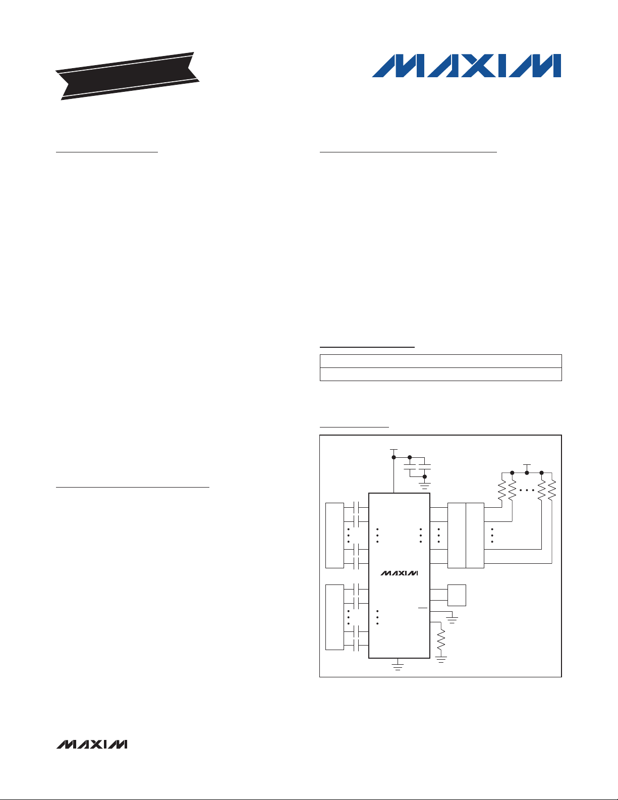
Typical Operating Circuit
3.3V
40 TQFN-EP*
V
= 3.3V
AVCC
MAX14886
Applications
Dual Graphics Notebook Computers
Dual Mode DisplayPort to HDMI External
Switches or Adapters
HDMI is a trademark of HDMI Licensing, LLC.
DisplayPort is a trademark of Video Electronics Standards
Association (VESA).
TMDS is a registered trademark of Silicon Image, Inc.
_______________________________________________________________ Maxim Integrated Products 1
100nF
A
DisplayPort
100nF
B
DisplayPort
D0AP
D0AN
CKAP
CKAN
D0BP
D0BN
CKBP
CKBN
V
CC
MAX14886
GND
D0CP
D0CN
CKCP
CKCN
SEL
EN1
EN2
ADJ
3.3kΩ
50Ω
HDMI SINK
HDMI CONNECTORMCU
For pricing, delivery, and ordering information, please contact Maxim Direct at 1-888-629-4642,
or visit Maxim’s website at www.maxim-ic.com.
Page 2

Dual DisplayPort Graphics Multiplexer
with HDMI Level Shifter
ABSOLUTE MAXIMUM RATINGS
(Voltages referenced to GND.)
VCC .......................................................................-0.3V to +4.0V
EN1, EN2, SEL, ADJ ................................ -0.3V to (VCC + 0.3V)
D_CP, D_CN, CKCP, CKCN Short-Circuit
Output Current ............................................................. Q30mA
All Other Pins Short-Circuit Current .................................. Q5mA
Continuous Power Dissipation (TA = +70NC)
TQFN (derate 35.7mW/NC above +70NC) ..................2857mW
Operating Temperature Range ............................. 0NC to +70NC
Storage Temperature Range ............................ -65NC to +150NC
Maximum Junction Temperature .....................................+150NC
Lead Temperature (soldering, 10s) ................................+300NC
Soldering Temperature (reflow) ......................................+260NC
MAX14886
PACKAGE THERMAL CHARACTERISTICS (Note 1)
TQFN
Junction-to-Ambient Thermal Resistance (qJA) ..........45°C/W
Junction-to-Case Thermal Resistance (qJC) .................2°C/W
Note 1: Package thermal resistances were obtained using method described in JEDEC specification JESD51-7, using a four-layer
board. For detailed information on package thermal considerations, refer to www.maxim-ic.com/thermal-tutorial.
Stresses beyond those listed under “Absolute Maximum Ratings” may cause permanent damage to the device. These are stress ratings only, and functional
operation of the device at these or any other conditions beyond those indicated in the operational sections of the specifications is not implied. Exposure to absolute
maximum rating conditions for extended periods may affect device reliability.
ELECTRICAL CHARACTERISTICS
(VCC = +3.3V, TA = 0NC to +70NC, R
PARAMETER SYMBOL CONDITIONS MIN TYP MAX UNITS
DC PERFORMANCE
Supply Voltage V
Supply Current I
Total Supply Current I
Shutdown Supply Current I
Single-Ended Input Termination
Resistance
Single-Ended Output Voltage
High
Single-Ended Output Voltage
Low
= 3.3kI, CCL = 100nF, typical values are at TA = +25NC.) (Note 2)
ADJ
CC
CC
GND
SHUT
R
IN
V
OH
V
OL
EN1 = high, EN2 = low
50I termination to AVCC, V
(Note 3)
EN1 = low or EN2 = high
DC 40 60
DC, V
DC, V
= +3.3V (Notes 3, 4)
AVCC
= +3.3V (Notes 3, 4)
AVCC
AVCC
= +3.3V
3 3.6 V
V
AVCC
- 0.01
V
AVCC
- 0.6
52.5 mA
105 mA
100
V
AVCC
+ 0.01
V
AVCC
- 0.45
FA
I
V
V
2
Page 3

Dual DisplayPort Graphics Multiplexer
with HDMI Level Shifter
ELECTRICAL CHARACTERISTICS (continued)
(VCC = +3.3V, TA = 0NC to +70NC, R
PARAMETER SYMBOL CONDITIONS MIN TYP MAX UNITS
AC PERFORMANCE
Differential Input Return Loss SDD11
Input Frequency Range f
Differential Input Range V
Differential Output Voltage V
Output Rise/Fall Time t
Deterministic Jitter t
Random Jitter t
Lane-to-Lane Skew t
Propagation Delay t
CONTROL LOGIC (EN1, EN2, SEL)
Input Logic-Low Voltage V
Input Logic-High Voltage V
Input Logic Hysteresis V
Input Pulldown/Pullup Resistor R
Shutdown Recovery Time t
TMDS Mux Switching Time t
ESD PROTECTION
All Pins Human Body Model ±8 kV
Note 2: All units are production tested at TA = +70NC. Specifications over temperature are guaranteed by design.
Note 3: AVCC is an external supply.
Note 4: Guaranteed by design; not production tested.
= 3.3kI, CCL = 100nF, typical values are at TA = +25NC.) (Note 2)
ADJ
150MHz P f P 1.25GHz
IN
IDIFF
ODIFF
R/F
DJ
RJ
SK
PD
HYST
IPULL
SHUT
MUX
Clock 25 225
Data 225 1125
200 1600 mV
50I single termination
20% to 80%, 2.25Gbps 80 ps
K28.5 pattern, up to 2.25Gbps (Note 4) 0.04 UI
D10.2 pattern, 2.25Gbps (Note 4) 1.1 ps
IL
IH
900 1250 mV
1.4 V
-8 dB
50 ps
250 ps
0.6 V
50 mV
400
20
50 ns
MAX14886
MHz
RMS
kI
Fs
3
Page 4

Dual DisplayPort Graphics Multiplexer
EYE DIAGRAM, VIN = 200mV
, 2.25Gbps,
with HDMI Level Shifter
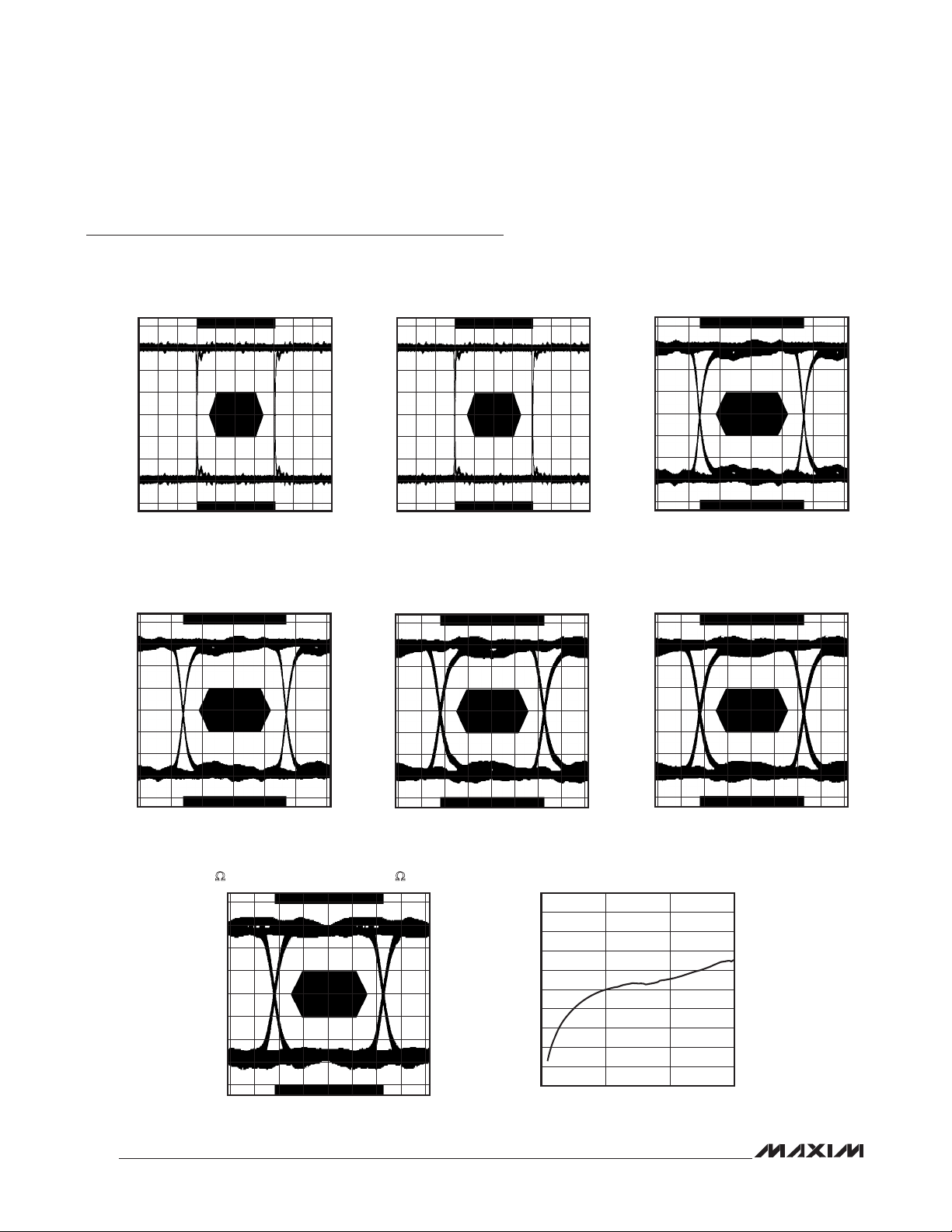
Typical Operating Characteristics
(VCC = +3.3V, TA = +25NC, R
EYE DIAGRAM, VIN = 1600mV
250Mbps, NO BACK TERMINATION,
25MHz CLOCK, 640 x 480, 8-BIT COLOR, 60Hz
800
600
MAX14886
400
200
0
-200
VOLTAGE (mV)
-400
-600
-800
-5
(ns)
= 3.3kI, unless otherwise noted.)
ADJ
P-P
,
EYE DIAGRAM, VIN = 200mV
250Mbps, NO BACK TERMINATION,
25MHz CLOCK, 640 x 480, 8-BIT COLOR, 60Hz
800
600
MAX14886 toc01
400
200
0
-200
VOLTAGE (mV)
-400
-600
-800
431 2-3 -2 -1 0-4
-5
(ns)
P-P
,
EYE DIAGRAM, VIN = 1600mV
1.5Gbps, NO BACK TERMINATION, 150MHz CLOCK
800
600
MAX14886 toc02
400
200
0
-200
VOLTAGE (mV)
-400
-600
-800
431 2-3 -2 -1 0-4
(ps)
400 6002000-200-400-600
P-P
,
MAX14886 toc03
EYE DIAGRAM, VIN = 200mV
1.5Gbps, NO BACK TERMINATION,
1080p, 8-BIT COLOR, 60Hz
800
600
400
200
0
-200
VOLTAGE (mV)
-400
-600
-800
,
P-P
EYE DIAGRAM, VIN = 1600mV
2.25Gbps, NO BACK TERMINATION
800
600
MAX14886 toc04
400
200
0
-200
VOLTAGE (mV)
-400
-600
-800
400 6002000-200-400-600
(ps)
P-P
400Ω BACK TERMINATION, RSET = 3kΩ, FIGURE 1
800
600
400
200
0
-200
VOLTAGE (mV)
-400
-600
-800
(ps)
MAX14886 toc07
300 4002000 100-200 -100-300-400
(ps)
MAGNITUDE (dB)
EYE DIAGRAM, VIN = 200mV
P-P
,
2.25Gbps, NO BACK TERMINATION,
225MHz CLOCK, 1080p, 12-BIT COLOR, 60Hz
800
600
MAX14886 toc05
400
200
0
-200
VOLTAGE (mV)
-400
-600
-800
300 4002000 100-200 -100-300-400
DIFFERENTIAL INPUT RETURN LOSS
vs. FREQUENCY
5
0
-5
-10
-15
-20
-25
-30
-35
-40
-45
0 3
FREQUENCY (GHz)
21
(ps)
MAX14886 toc08
P-P
300 4002000 100-200 -100-300-400
,
MAX14886 toc06
4
Page 5

Dual DisplayPort Graphics Multiplexer
with HDMI Level Shifter
Pin Configuration
MAX14886
TOP VIEW
V
GND
ADJ
SEL
GND
V
EN2
EN1
GND
V
D1AN
31
CC
32
33
34
35
36
CC
37
38
39
40
CC
1 2
D0AP
D1BP
D1BN
D1AP
GND
27282930 26 24 23 22
MAX14886
+
4 5 6 7
3
GND
D0BP
D0AN
D0BN
25
D2AN
CKAP
D2AP
D2BN
*EP
8 9 10
CKBP
CKAN
D2BP
CKBN
GND
21
20
D2CP
19
D2CN
D1CP
18
D1CN
17
16
V
CC
D0CP
15
14
D0CN
CKCP
13
12
CKCN
11
GND
GND
TQFN
(5mm × 5mm × 0.75mm)
*CONNECT EP TO GND.
Pin Description
PIN NAME FUNCTION
1 D0AP Noninverting Input D0 for Channel A
2 D0AN Inverting Input D0 for Channel A
3 D0BP Noninverting Input D0 for Channel B
4 D0BN Inverting Input D0 for Channel B
5, 10,
11, 21,
26, 32,
GND Ground
35, 39
6 CKAP Noninverting Input Clock for Channel A
7 CKAN Inverting Input Clock for Channel A
8 CKBP Noninverting Input Clock for Channel B
9 CKBN Inverting Input Clock for Channel B
12 CKCN Inverting Output Clock
13 CKCP Noninverting Output Clock
14 D0CN Inverting Output D0
15 D0CP Noninverting Output D0
Power-Supply Voltage. Bypass VCC
16, 31,
36, 40
V
to GND with low-ESR 10nF and
4.7FF ceramic capacitors in parallel
CC
as close as possible to the device.
Recommended on each VCC pin.
17 D1CN Inverting Output D1
PIN NAME FUNCTION
18 D1CP Noninverting Output D1
19 D2CN Inverting Output D2
20 D2CP Noninverting Output D2
22 D2BP Noninverting Input D2 for Channel B
23 D2BN Inverting Input D2 for Channel B
24 D2AP Noninverting Input D2 for Channel A
25 D2AN Inverting Input D2 for Channel A
27 D1BP Noninverting Input D1 for Channel B
28 D1BN Inverting Input D1 for Channel B
29 D1AP Noninverting Input D1 for Channel A
30 D1AN Inverting Input D1 for Channel A
33 ADJ Output Level Adjust
34 SEL
Mux Select Input. SEL is internally
pulled down by a 400kI (typ) resistor.
Active-Low Enable Input. EN2 is inter-
37
EN2
nally pulled up by a 400kI (typ)
resistor.
Active-High Enable Input. EN1 is
38 EN1
internally pulled down by a 400kI (typ)
resistor.
— EP Exposed Pad. Connect EP to GND.
5
Page 6

Dual DisplayPort Graphics Multiplexer
with HDMI Level Shifter
Functional Diagram/Truth Tables
V
CC
V
CC
50Ω
D2AP
D2AN
MAX14886
50Ω
D2BP
D2BN
50Ω
D1AP
D1AN
50Ω
D1BP
D1BN
50Ω
D0AP
D0AN
50Ω
V
CC
50Ω
V
CC
50Ω
V
CC
50Ω
V
CC
50Ω
V
CC
MULTIPLEXER/
LIMITING
AMPLIFIER
MAX14886
D2CP
D2CN
D1CP
D1CN
D0CP
D0CN
EN1
EN2
FUNCTION
0/Unconnected X Shutdown
X 1/Unconnected Shutdown
1 0 Active
X = Don’t care.
SEL D_A_, CKA_ D_B_, CKB_
0/Unconnected On Off
1 Off On
X = Don’t care.
50Ω
D0BP
D0BN
50Ω
CKAP
CKAN
50Ω
CKBP
CKBN
50Ω
CKCP
V
CC
50Ω
V
CC
50Ω
CONTROL
EN1 EN2 SEL ADJGND
CKCN
6
Page 7

Dual DisplayPort Graphics Multiplexer
Detailed Description
The MAX14886 is a high-speed, low-skew, active
redriver multiplexer designed to switch and amplify
TMDS-formatted signals. Input buffers have 50I HDMIcompliant terminations to VCC (see the Functional
Diagram/Truth Tables), allowing either DC-coupling to
an HDMI source or AC-coupling to a DisplayPort source.
Signals from the input buffers are multiplexed and
redriven by the limiting amplifier and an open-collector
output buffer. The HDMI monitor sink is DC-coupled to
the outputs and provides DC bias.
Both TMDS clock and data are multiplexed and redriven
to full HDMI v.1.4 levels with low skew and jitter to
guarantee mask compliance at an external HDMI connector. The device is VESA DisplayPort Interoperability
Guideline v.1.1a-compliant and integrates seamlessly
with an external HDMI connector on the motherboard.
The low-frequency signals (DDC, CEC, and HPD) can be
handled by external low-cost logic.
The device accommodates differential inputs as low as
200mV and drives differential TMDS outputs to 1000mV
(typ). A precision resistor on the output level adjust pin
(ADJ) allows differential output back-termination resistors of 400I (typ) to better meet HDMI mask jitter compliance, while maintaining full TMDS swing requirements.
This device also features both active-high and activelow enable inputs. One of the enable inputs can be
connected to either VCC or GND, while the other can be
used to control the device (see the Functional Diagram/
Truth Tables and Enable Inputs (EN1, EN2) section). This
eliminates any issues with logic sense and the need for
an inverter.
Level Translation
The device accepts two sets of four differential
DisplayPort-level TMDS-formatted inputs, each with
magnitudes as low as 200mV. The selected channel is
translated to full HDMI TMDS levels that are HDMI v.1.4
port mask-compliant up to 2.25Gbps.
Enable Inputs (EN1, EN2)
The device features both an active-high enable input
(EN1) and an active-low enable input (EN2) that can be
controlled by LVCMOS or LVTTL. EN1 has an internal
400kI (typ) pulldown resistor, and EN2 has an internal
400kI (typ) pullup resistor. When EN1 is driven low or
left unconnected, or EN2 is driven high or left unconnected, the device enters low-power shutdown mode.
For normal operation drive both EN1 high and EN2 low.
See the Functional Diagram/Truth Tables.
with HDMI Level Shifter
MAX14886
Only one input is necessary to control the device. If
active-high enable is desired, connect EN2 to GND and
use EN1 to control the device. Similarly, for active-low
enable, connect EN1 to VCC and use EN2 to control the
device.
Note: The monitor sink termination must be present and
powered before enabling the device (see the Control
Sequence section and Figure 2).
Digital Control Input (SEL)
The device provides two sets of 4 channels for all the differential signals required by HDMI connections. The SEL
input controls which channel is translated to the output
channel (see the Functional Diagram/Truth Tables). An
internal 400kI pulldown resistor guarantees that channel
A is translated to the output if the SEL pin is not externally
driven.
Output Level Adjust (ADJ)
The level-shifter’s output current and output signal swing
are set with an external ±1% precision 3.3kI (typ) resistor. If a double output termination (400I typ) is desired
for signal integrity reasons, the ADJ resistor value can be
decreased to maintain a desired output swing (Figure 1).
Applications Information
HDMI Driver
The device’s high-speed, low-skew, active redriver
multiplexer is ideal for switching between outputs of
dual-graphics systems and signal conditioning to meet
HDMI v.1.4 compliance at an external HDMI connector
(Figure 1). It is well suited for switching between integrated (e.g., Intel or AMD) and discrete graphics (e.g.,
NVIDIA or ATI GPU). The device is VESA DisplayPort
Interoperability Guideline v.1.1a-compliant (requires
external DDC logic) and integrates seamlessly with an
external HDMI connector on the motherboard.
Output Termination
Outputs are terminated in normal use by the HDMI monitor. For 50I test equipment purposes, terminate each
output with a high-frequency bias-T that has an inductor
in series with a 50I resistor to VCC.
Control Sequence
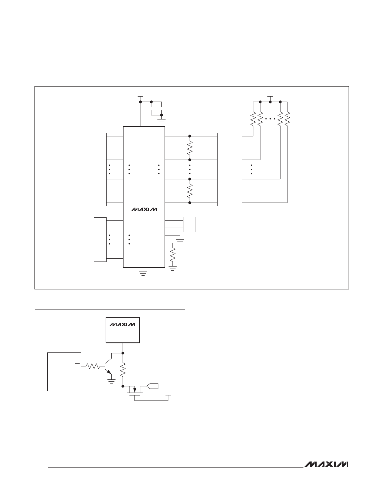
The monitor sink termination must be present and powered before enabling the device. A simple circuit can
be added to protect the device by forcing hot-plug
detection (HPD) to be present before the part is enabled
(Figure 2).
7
Page 8

Dual DisplayPort Graphics Multiplexer
with HDMI Level Shifter
50Ω
V
AVCC
D0AP
3.3V
V
CC
D0CP
400Ω
MAX14886
D0AN
D0CN
= 3.3V
SOURCE A
SOURCE B
FOR DisplayPort SOURCE, ADD AC-COUPLING CAPACITORS.
CKAP
CKAN
D0BP
D0BN
CKBP
CKBN
CKCP
CKCN
MAX14886
SEL
EN1
EN2
ADJ
3kΩ
GND
Figure 1. HDMI Driver Application with Output Back Termination
MAX14886
EN1
CONTROL CPU
GPIO
HPD
10k
Ω
EN
10kΩ
N
HPD
+3.3V
Figure 2. Control Sequence Protection Circuit
HDMI SINK
HDMI CONNECTOR
400Ω
MCU
Power-Supply Bypassing
Adequate power-supply bypassing is necessary to maximize performance and noise immunity. Bypass each
VCC pin to GND with high-frequency, low-ESR, X7R/X5R
10nF and 4.7FF surface-mount ceramic capacitors as
close as possible to the device.
Printed Circuit Board (PCB) Traces
Input and output trace characteristics affect the performance of the device. Connect each of the inputs and
outputs to a 50I characteristic impedance trace in to
minimize reflections. Avoid discontinuities in differential
impedance and maximize common-mode noise immunity by maintaining the distance between differential traces
and avoiding sharp corners. Minimize the number of vias
to prevent impedance discontinuities. Reduce reflections by maintaining the 50I characteristic impedance
through connectors and across cables. Minimize skew
by matching the electrical length of the traces.
8
Page 9

Dual DisplayPort Graphics Multiplexer
Exposed-Pad Package
The exposed-pad, 40-pin TQFN package incorporates
features that provide a very low thermal resistance
path for heat removal from the IC. The exposed pad
on the device must be soldered to the circuit board
ground plane for proper electrical and thermal performance. For more informa tion on exposed-pad packages, refer to Application Note 862: HFAN-08.1: Thermal
Considerations of QFN and Other Exposed-Paddle
Packages.
with HDMI Level Shifter
Chip Information
PROCESS: BiCMOS
Package Information
For the latest package outline information and land patterns
(footprints), go to www.maxim-ic.com/packages. Note that a
“+”, “#”, or “-” in the package code indicates RoHS status only.
Package drawings may show a different suffix character, but
the drawing pertains to the package regardless of RoHS status.
PACKAGE
TYPE
40 TQFN-EP T4055+2
PACKAGE
CODE
OUTLINE
NO.
21-0140 90-0002
LAND
PATTERN NO.
MAX14886
9
Page 10

Dual DisplayPort Graphics Multiplexer
with HDMI Level Shifter
Revision History
REVISION
NUMBER
0 12/10 Initial release —
REVISION
DATE
MAX14886
DESCRIPTION
PAGES
CHANGED
Maxim cannot assume responsibility for use of any circuitry other than circuitry entirely embodied in a Maxim product. No circuit patent licenses are implied.
Maxim reserves the right to change the circuitry and specifications without notice at any time.
10 Maxim Integrated Products, 120 San Gabriel Drive, Sunnyvale, CA 94086 408-737-7600
©
2010 Maxim Integrated Products Maxim is a registered trademark of Maxim Integrated Products, Inc.
 Loading...