

19-0122; Rev 5; 2/96
Low-Power, Slew-Rate-Limited
RS-485/RS-422 Transceivers
_______________General Description
The MAX481, MAX483, MAX485, MAX487–MAX491, and
MAX1487 are low-power transceivers for RS-485 and RS422 communication. Each part contains one driver and one
receiver. The MAX483, MAX487, MAX488, and MAX489
feature reduced slew-rate drivers that minimize EMI and
reduce reflections caused by improperly terminated cables,
thus allowing error-free data transmission up to 250kbps.
The driver slew rates of the MAX481, MAX485, MAX490,
MAX491, and MAX1487 are not limited, allowing them to
transmit up to 2.5Mbps.
These transceivers draw between 120µA and 500µA of
supply current when unloaded or fully loaded with disabled
drivers. Additionally, the MAX481, MAX483, and MAX487
have a low-current shutdown mode in which they consume
only 0.1µA. All parts operate from a single 5V supply.
Drivers are short-circuit current limited and are protected
against excessive power dissipation by thermal shutdown
circuitry that places the driver outputs into a high-impedance state. The receiver input has a fail-safe feature that
guarantees a logic-high output if the input is open circuit.
The MAX487 and MAX1487 feature quarter-unit-load
receiver input impedance, allowing up to 128 MAX487/
MAX1487 transceivers on the bus. Full-duplex communications are obtained using the MAX488–MAX491, while
the MAX481, MAX483, MAX485, MAX487, and MAX1487
are designed for half-duplex applications.
____________________________Features
♦ In µMAX Package: Smallest 8-Pin SO
♦ Slew-Rate Limited for Error-Free Data
Transmission (MAX483/487/488/489)
♦ 0.1µA Low-Current Shutdown Mode
(MAX481/483/487)
♦ Low Quiescent Current:
120µA (MAX483/487/488/489)
230µA (MAX1487)
300µA (MAX481/485/490/491)
♦ -7V to +12V Common-Mode Input Voltage Range
♦ Three-State Outputs
♦ 30ns Propagation Delays, 5ns Skew
(MAX481/485/490/491/1487)
♦ Full-Duplex and Half-Duplex Versions Available
♦ Operate from a Single 5V Supply
♦ Allows up to 128 Transceivers on the Bus
(MAX487/MAX1487)
♦ Current-Limiting and Thermal Shutdown for
Driver Overload Protection
MAX481/MAX483/MAX485/MAX487–MAX491/MAX1487
________________________Applications
Low-Power RS-485 Transceivers
Low-Power RS-422 Transceivers
Level Translators
Transceivers for EMI-Sensitive Applications
Industrial-Control Local Area Networks
______________Ordering Information
PART TEMP. RANGE PIN-PACKAGE
MAX481CPA
MAX481CSA 0°C to +70°C 8 SO
MAX481CUA 0°C to +70°C 8 µMAX
MAX481C/D 0°C to +70°C Dice*
Ordering Information continued at end of data sheet.
0°C to +70°C 8 Plastic DIP
* Contact factory for dice specifications.
______________________________________________________________Selection Table
PART
NUMBER
MAX481
MAX483
MAX485
MAX487
MAX488
MAX489
MAX490
MAX491
MAX1487
HALF/FULL
DUPLEX
Half
Half
Half
Half
Full
Full
Full
Full
Half
DATA RATE
(Mbps)
2.5
0.25
2.5
0.25
0.25
0.25
2.5
2.5
2.5
________________________________________________________________
SLEW-RATE
LIMITED
No
Yes
No
Yes
Yes
Yes
No
No
No
LOW-POWER
SHUTDOWN
Yes
Yes
No
Yes
No
No
No
No
No
RECEIVER/
DRIVER
ENABLE
Yes
Yes
Yes
Yes
No
Yes
No
Yes
Yes
QUIESCENT
CURRENT
(µA)
300
120
300
120
120
120
300
300
230
NUMBER OF
TRANSMITTERS
ON BUS
32
32
32
128
32
32
32
32
128
PIN
COUNT
8
8
8
8
8
14
8
14
8
Maxim Integrated Products
1
For free samples & the latest literature: http://www.maxim-ic.com, or phone 1-800-998-8800
Low-Power, Slew-Rate-Limited
RS-485/RS-422 Transceivers
ABSOLUTE MAXIMUM RATINGS
Supply Voltage (VCC).............................................................12V
Control Input Voltage (–R—E–, DE)...................-0.5V to (V
Driver Input Voltage (DI).............................-0.5V to (V
Driver Output Voltage (A, B)...................................-8V to +12.5V
Receiver Input Voltage (A, B).................................-8V to +12.5V
Receiver Output Voltage (RO).....................-0.5V to (V
Continuous Power Dissipation (T
8-Pin Plastic DIP (derate 9.09mW/°C above +70°C) ....727mW
14-Pin Plastic DIP (derate 10.00mW/°C above +70°C)..800mW
8-Pin SO (derate 5.88mW/°C above +70°C).................471mW
Stresses beyond those listed under “Absolute Maximum Ratings” may cause permanent damage to the device. These are stress ratings only, and functional
operation of the device at these or any other conditions beyond those indicated in the operational sections of the specifications is not implied. Exposure to
absolute maximum rating conditions for extended periods may affect device reliability.
= +70°C)
A
CC
CC
CC
+ 0.5V)
+ 0.5V)
+0.5V)
DC ELECTRICAL CHARACTERISTICS
(VCC= 5V ±5%, TA= T
Differential Driver Output (no load)
Differential Driver Output
(with load)
Change in Magnitude of Driver
Differential Output Voltage for
Complementary Output States
Driver Common-Mode Output
Voltage
Change in Magnitude of Driver
Common-Mode Output Voltage
for Complementary Output States
Input High Voltage
Input Low Voltage
Input Current
Input Current
(A, B)
Receiver Differential Threshold
Voltage
Receiver Input Hysteresis
Receiver Output High Voltage
Receiver Output Low Voltage
Three-State (high impedance)
Output Current at Receiver
Receiver Input Resistance
MAX481/MAX483/MAX485/MAX487–MAX491/MAX1487
MIN
to T
, unless otherwise noted.) (Notes 1, 2)
MAX
OD1
V
I
V
OZR
R
OD2
OC
IN1
IN2
OH
R = 50Ω (RS-422)
R = 27Ω (RS-485), Figure 4
R = 27Ω or 50Ω, Figure 4
OD
R = 27Ω or 50Ω, Figure 4
R = 27Ω or 50Ω, Figure 4
OD
DE, DI, –R—E
IH
DE, DI, –R—E
IL
DE, DI, –R—E
DE = 0V;
VCC= 0V or 5.25V,
all devices except
MAX487/MAX1487
MAX487/MAX1487,
DE = 0V, VCC= 0V or 5.25V
-7V ≤ VCM≤ 12V
TH
VCM= 0V
TH
IO= -4mA, VID= 200mV
IO = 4mA, VID= -200mV
OL
0.4V ≤ VO≤ 2.4V
-7V ≤ VCM≤ 12V, all devices except
MAX487/MAX1487
IN
CM
–
–
–
≤ 12V, MAX487/MAX1487
14-Pin SO (derate 8.33mW/°C above +70°C)...............667mW
8-Pin µMAX (derate 4.1mW/°C above +70°C)..............830mW
8-Pin CERDIP (derate 8.00mW/°C above +70°C).........640mW
14-Pin CERDIP (derate 9.09mW/°C above +70°C).......727mW
Operating Temperature Ranges
MAX4_ _C_ _/MAX1487C_ A ...............................0°C to +70°C
MAX4_ _E_ _/MAX1487E_ A.............................-40°C to +85°C
MAX4_ _MJ_/MAX1487MJA ...........................-55°C to +125°C
Storage Temperature Range.............................-65°C to +160°C
Lead Temperature (soldering, 10sec).............................+300°C
CONDITIONS
2
1.5 5
VIN= 12V
VIN= -7V
VIN= 12V
VIN= -7V
3.5V
1.0
-0.8
0.25
-0.2
0.4V
UNITSMIN TYP MAXSYMBOLPARAMETER
V5V
V
V0.2∆V
V3V
V0.2∆V
V2.0V
V0.8V
µA±2I
mA
mA
V-0.2 0.2
mV70∆V
V
V
µA±1I
kΩ12
kΩ48-7V ≤ V
2 _______________________________________________________________________________________
Low-Power, Slew-Rate-Limited
RS-485/RS-422 Transceivers
DC ELECTRICAL CHARACTERISTICS (continued)
(VCC= 5V ±5%, TA= T
No-Load Supply Current
(Note 3)
Supply Current in Shutdown
Driver Short-Circuit Current,
VO= High
Driver Short-Circuit Current,
VO= Low
Receiver Short-Circuit Current
MIN
to T
, unless otherwise noted.) (Notes 1, 2)
MAX
MAX488/MAX489,
DE, DI, –R—E–= 0V or V
MAX490/MAX491,
DE, DI, –R—E–= 0V or V
MAX481/MAX485,
–R—E–
I
CC
SHDN
OSD1
OSD2
I
OSR
= 0V or V
MAX1487,
–R—E–
= 0V or V
MAX483/MAX487,
–R—E–
= 0V or V
CC
CC
CC
CC
CONDITIONS UNITSMIN TYP MAXSYMBOLPARAMETER
CC
CC
DE = V
CC
120 250
300 500
500 900
300 500DE = 0V
DE = V
DE = 0V
DE = 5V
DE = 0V
CC
MAX483
MAX487
CC
300 500
230 400
350 650
250 400
120 250
0.1 10I
7950V ≤ VO≤ V
SWITCHING CHARACTERISTICS—MAX481/MAX485, MAX490/MAX491, MAX1487
(VCC= 5V ±5%, TA= T
Driver Input to Output
Driver Output Skew to Output
Driver Rise or Fall Time
Driver Enable to Output High
Driver Enable to Output Low
Driver Disable Time from Low
Driver Disable Time from High
Receiver Input to Output
| t
- t
PLH
| Differential
PHL
Receiver Skew
Receiver Enable to Output Low
Receiver Enable to Output High
Receiver Disable Time from Low
Receiver Disable Time from High
Maximum Data Rate
Time to Shutdown
MIN
to T
, unless otherwise noted.) (Notes 1, 2)
MAX
PLH
PHL
SKEW
Figures 6 and 8, R
CL1= CL2= 100pF
Figures 6 and 8, R
Figures 6 and 8,
R
t
, t
R
F
DIFF
= 54Ω,
CL1= CL2= 100pF
Figures 7 and 9, CL= 100pF, S2 closed
ZH
Figures 7 and 9, CL= 100pF, S1 closed
ZL
Figures 7 and 9, CL= 15pF, S1 closed
LZ
Figures 7 and 9, CL= 15pF, S2 closed
HZ
Figures 6 and 10,
R
t
PLH
, t
PHL
DIFF
= 54Ω,
CL1= CL2= 100pF
t
SKD
MAX
SHDN
Figures 6 and 10, R
CL1= CL2= 100pF
Figures 5 and 11, CRL= 15pF, S1 closed
ZL
Figures 5 and 11, CRL= 15pF, S2 closed
ZH
Figures 5 and 11, CRL= 15pF, S1 closed
LZ
Figures 5 and 11, CRL= 15pF, S2 closed
HZ
MAX481 (Note 5)
CONDITIONS
DIFF
= 54Ω,
10 30 60t
10 30 60t
= 54Ω, CL1= CL2= 100pF
DIFF
MAX481, MAX485, MAX1487
MAX490C/E, MAX491C/E
MAX490M, MAX491M
31540
51525
31540
510t
40 70t
40 70t
40 70t
MAX481, MAX485, MAX1487
20 90 200
MAX490C/E, MAX491C/E 20 90 150
MAX490M, MAX491M
= 54Ω,
DIFF
20 90 200
13
20 50t
MAX481/MAX483/MAX485/MAX487–MAX491/MAX1487
µA
µAMAX481/483/487, DE = 0V, –R—E–= V
mA35 250-7V ≤ VO≤12V (Note 4)I
mA35 250-7V ≤ VO≤12V (Note 4)I
mA
UNITSMIN TYP MAXSYMBOLPARAMETER
ns
ns
ns
ns
ns
ns40 70t
ns
ns
ns
ns20 50t
ns20 50t
ns
ns20 50t
Mbps2.5f
ns50 200 600t
_______________________________________________________________________________________ 3
Low-Power, Slew-Rate-Limited
RS-485/RS-422 Transceivers
SWITCHING CHARACTERISTICS—MAX481/MAX485, MAX490/MAX491, MAX1487 (continued)
(VCC= 5V ±5%, TA= T
Driver Enable from Shutdown to
Output High (MAX481)
Driver Enable from Shutdown to
Output Low (MAX481)
Receiver Enable from Shutdown
to Output High (MAX481)
Receiver Enable from Shutdown
to Output Low (MAX481)
MIN
to T
, unless otherwise noted.) (Notes 1, 2)
MAX
ZH(SHDN)
ZL(SHDN)
ZH(SHDN)
t
ZL(SHDN)
Figures 7 and 9, CL= 100pF, S2 closed
Figures 7 and 9, CL= 100pF, S1 closed
Figures 5 and 11, CL= 15pF, S2 closed,
A - B = 2V
Figures 5 and 11, CL= 15pF, S1 closed,
B - A = 2V
CONDITIONS
300 1000
UNITSMIN TYP MAXSYMBOLPARAMETER
ns40 100t
ns40 100t
ns300 1000t
ns
SWITCHING CHARACTERISTICS—MAX483, MAX487/MAX488/MAX489
(VCC= 5V ±5%, TA= T
Driver Input to Output
Driver Output Skew to Output ns100 800
Driver Rise or Fall Time
Driver Enable to Output High
Driver Enable to Output Low
Driver Disable Time from Low
Driver Disable Time from High
Receiver Input to Output
I t
- t
PLH
I Differential
PHL
Receiver Skew
Receiver Enable to Output Low
Receiver Enable to Output High
Receiver Disable Time from Low
Receiver Disable Time from High
Maximum Data Rate
Time to Shutdown
Driver Enable from Shutdown to
Output High
Driver Enable from Shutdown to
Output Low
Receiver Enable from Shutdown
to Output High
Receiver Enable from Shutdown
to Output Low
MIN
to T
, unless otherwise noted.) (Notes 1, 2)
MAX
t
PLH
t
PHL
t
SKEW
ZH
ZL
LZ
HZ
t
PLH
t
PHL
t
SKD
ZL
ZH
LZ
HZ
MAX
SHDN
t
ZH(SHDN)
t
ZL(SHDN)
t
ZH(SHDN)
t
ZL(SHDN)
Figures 6 and 8, R
CL1= CL2= 100pF
Figures 6 and 8, R
CL1= CL2= 100pF
Figures 6 and 8, R
F
CL1= CL2= 100pF
Figures 7 and 9, CL= 100pF, S2 closed
Figures 7 and 9, CL= 100pF, S1 closed
Figures 7 and 9, CL= 15pF, S1 closed
Figures 7 and 9, CL= 15pF, S2 closed
Figures 6 and 10, R
CL1= CL2= 100pF
Figures 6 and 10, R
CL1= CL2= 100pF
Figures 5 and 11, CRL= 15pF, S1 closed
Figures 5 and 11, CRL= 15pF, S2 closed
Figures 5 and 11, CRL= 15pF, S1 closed
Figures 5 and 11, CRL= 15pF, S2 closed
t
, t
PLH
PHL
MAX483/MAX487, Figures 7 and 9,
CL= 100pF, S2 closed
MAX483/MAX487, Figures 7 and 9,
CL= 100pF, S1 closed
MAX483/MAX487, Figures 5 and 11,
CL= 15pF, S2 closed
MAX483/MAX487, Figures 5 and 11,
CL= 15pF, S1 closed
CONDITIONS
= 54Ω,
DIFF
= 54Ω,
DIFF
= 54Ω,
DIFF
= 54Ω,
DIFF
= 54Ω,
DIFF
< 50% of data period
250 800 2000
250 800 2000
250 2000t
300 3000t
250 2000
250 2000
100
20 50t
UNITSMIN TYP MAXSYMBOLPARAMETER
ns
ns250 2000tR, t
ns
ns250 2000t
ns300 3000t
ns
ns
ns
ns20 50t
ns20 50t
ns
ns20 50t
kbps250f
ns50 200 600MAX483/MAX487 (Note 5) t
ns2000
ns2000
ns2500
ns2500
MAX481/MAX483/MAX485/MAX487–MAX491/MAX1487
4 _______________________________________________________________________________________
Low-Power, Slew-Rate-Limited
RS-485/RS-422 Transceivers
NOTES FOR ELECTRICAL/SWITCHING CHARACTERISTICS
Note 1: All currents into device pins are positive; all currents out of device pins are negative. All voltages are referenced to device
ground unless otherwise specified.
Note 2: All typical specifications are given for V
= 5V and TA= +25°C.
CC
Note 3: Supply current specification is valid for loaded transmitters when DE = 0V.
Note 4: Applies to peak current. See
Typical Operating Characteristics.
Note 5: The MAX481/MAX483/MAX487 are put into shutdown by bringing–R—E–high and DE low. If the inputs are in this state for less
than 50ns, the parts are guaranteed not to enter shutdown. If the inputs are in this state for at least 600ns, the parts are
guaranteed to have entered shutdown. See
Low-Power Shutdown Mode
section.
__________________________________________Typical Operating Characteristics
(VCC= 5V, TA = +25°C, unless otherwise noted.)
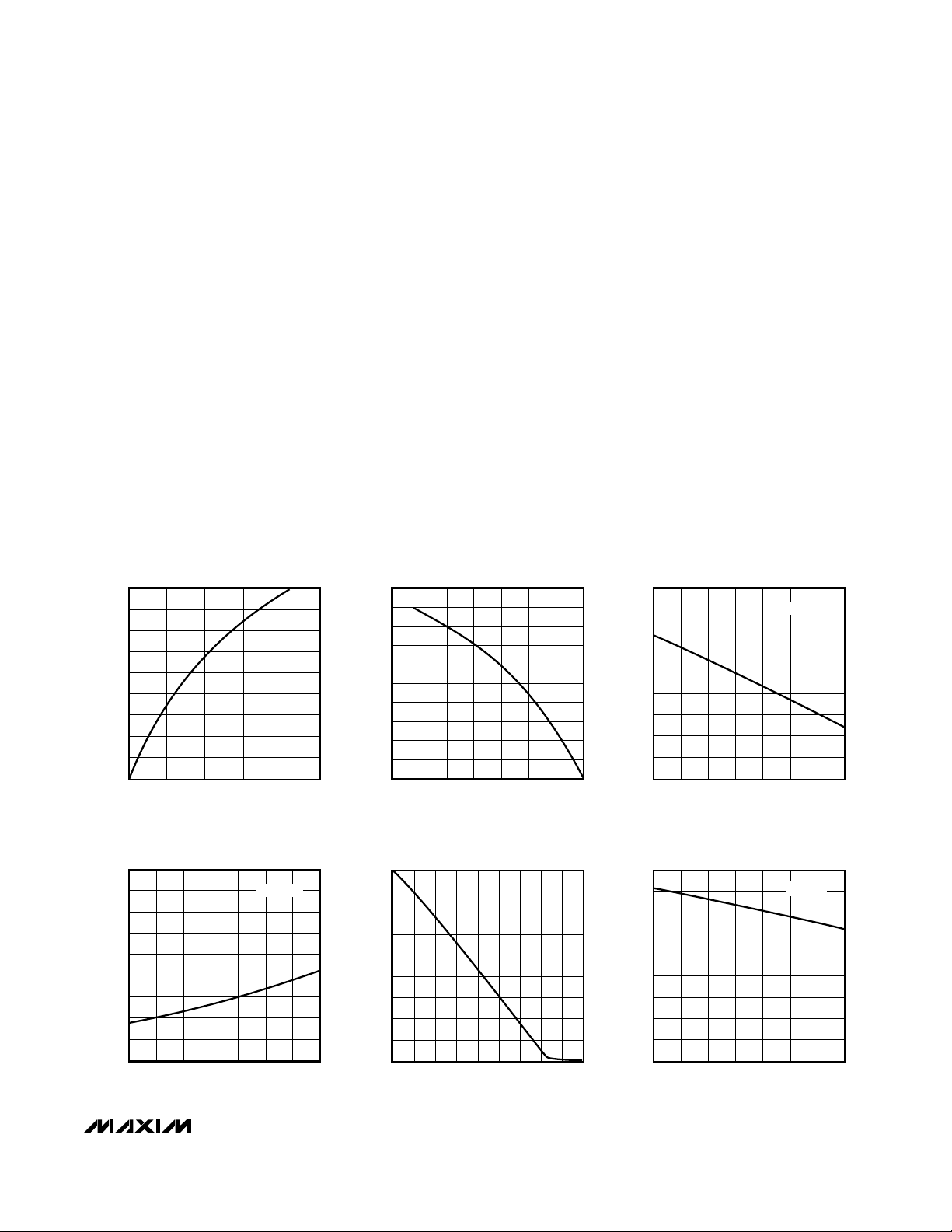
OUTPUT CURRENT vs.
RECEIVER OUTPUT LOW VOLTAGE
45
40
35
30
25
20
15
OUTPUT CURRENT (mA)
10
5
0
0.5 1.0 2.0
0 2.5
OUTPUT LOW VOLTAGE (V)
1.5
-20
-18
MAX481-01
-16
-14
-12
-10
-8
-6
OUTPUT CURRENT (mA)
-4
-2
0
1.5 2.0 3.0 5.0
OUTPUT CURRENT vs.
RECEIVER OUTPUT HIGH VOLTAGE
2.5 4.0
OUTPUT HIGH VOLTAGE (V)
3.5 4.5
RECEIVER OUTPUT HIGH VOLTAGE vs.
4.8
4.6
MAX481-02
4.4
4.2
4.0
3.8
3.6
3.4
OUTPUT HIGH VOLTAGE (V)
3.2
3.0
-50 -25 25 75
TEMPERATURE
IRO = 8mA
050
TEMPERATURE (°C)
100
125
MAX481/MAX483/MAX485/MAX487–MAX491/MAX1487
MAX481-03
RECEIVER OUTPUT LOW VOLTAGE vs.
TEMPERATURE
0.9
0.8
0.7
0.6
0.5
0.4
0.3
0.2
OUTPUT LOW VOLTAGE (V)
0.1
0
-50 -25 25 75
050
TEMPERATURE (°C)
_______________________________________________________________________________________
IRO = 8mA
100
125
90
MAX481-04
80
70
60
50
40
30
OUTPUT CURRENT (mA)
20
10
0
DRIVER OUTPUT CURRENT vs.
DIFFERENTIAL OUTPUT VOLTAGE
0 1.0 3.0 4.5
0.5 1.5 2.5 3.5
DIFFERENTIAL OUTPUT VOLTAGE (V)
2.0 4.0
DRIVER DIFFERENTIAL OUTPUT VOLTAGE
vs. TEMPERATURE
2.4
2.3
MAX481-05
2.2
2.1
2.0
1.9
1.8
1.7
DIFFERENTIAL OUTPUT VOLTAGE (V)
1.6
1.5
-50 -25 25 125
075
TEMPERATURE (°C)
R = 54Ω
10050
MAX481-06
5

Low-Power, Slew-Rate-Limited
RS-485/RS-422 Transceivers
____________________________Typical Operating Characteristics (continued)
(VCC= 5V, TA = +25°C, unless otherwise noted.)
OUTPUT CURRENT vs.
DRIVER OUTPUT LOW VOLTAGE
140
120
100
80
60
40
OUTPUT CURRENT (mA)
20
0
24
08
OUTPUT LOW VOLTAGE (V)
6
10
MAX483/MAX487–MAX489
SUPPLY CURRENT vs. TEMPERATURE
600
500
400
300
MAX487; DE = VCC, RE = X
200
MAX483/MAX487; DE = RE = 0,
MAX488/MAX489; DE = RE = X
SUPPLY CURRENT (µA)
100
MAX483/MAX487; DE = 0, RE = V
0
-50 -25 50 100
-120
MAX481-07
-100
-80
-60
-40
OUTPUT CURRENT (mA)
-20
0
12
MAX483; DE = VCC, RE = X
0
TEMPERATURE (°C)
-7 -5 -1 5
25 75
OUTPUT CURRENT vs.
DRIVER OUTPUT HIGH VOLTAGE
-6 -4 -2 0 2 4
-3 1
OUTPUT HIGH VOLTAGE (V)
SUPPLY CURRENT vs. TEMPERATURE
600
MAX481-12
500
400
MAX1487; DE = VCC, RE = X
300
200
MAX1487; DE = 0V, RE = X
SUPPLY CURRENT (µA)
100
CC
125
0
-40-60 -20 40 100 120
3
SUPPLY CURRENT vs. TEMPERATURE
600
MAX481-08
500
400
300
200
SUPPLY CURRENT (µA)
100
0
-50 -25 50 100
MAX1487
20 60 80
0
TEMPERATURE (°C)
MAX481/MAX485/MAX490/MAX491
MAX481/MAX485; DE = VCC, RE = X
MAX485; DE = 0, RE = X,
MAX481; DE = RE = 0
MAX490/MAX491; DE = RE = X
MAX481; DE = 0, RE = V
0
TEMPERATURE (°C)
140
CC
25 75
MAX481-13
MAX481-11
125
MAX481/MAX483/MAX485/MAX487–MAX491/MAX1487
6 _______________________________________________________________________________________
Low-Power, Slew-Rate-Limited
RS-485/RS-422 Transceivers
______________________________________________________________Pin Description
PIN
MAX481/MAX483/
MAX485/MAX487/
MAX1487
DIP/SO DIP/SO
2 3
3 4
4 5
5 6, 7 Ground
— 9 Noninverting Driver Output
— 10 Inverting Driver Output
6 — Noninverting Receiver Input and Noninverting Driver Output
µMAX
4
5
6
7
—
—
8
MAX488/
MAX490
DIP/SO
µMAX
2 RO
—
—
—
—
3
4
5
6
—
—
MAX489/
MAX491
431 2
5
6
7
8
NAME
–R—E–
DE
DI
GND
Y
Z
A
FUNCTION
FUNCTIONNAME
Receiver Output: If A > B by 200mV, RO will be high;
If A < B by 200mV, RO will be low.
Receiver Output Enable. RO is enabled when–R—E–is low; RO is
high impedance when–R—E–is high.
Driver Output Enable. The driver outputs, Y and Z, are enabled
by bringing DE high. They are high impedance when DE is low. If
the driver outputs are enabled, the parts function as line drivers.
While they are high impedance, they function as line receivers if
–R—E–
is low.
Driver Input. A low on DI forces output Y low and output Z high.
Similarly, a high on DI forces output Y high and output Z low.
MAX481/MAX483/MAX485/MAX487–MAX491/MAX1487
—
—
2
A
1
3
CC
Positive Supply: 4.75V ≤ VCC≤ 5.25V
— 12 Noninverting Receiver Input
7 — — B Inverting Receiver Input and Inverting Driver Output
— 7 11 B Inverting Receiver Input
8 1 14 V
— — 1, 8, 13 N.C. No Connect—not internally connected
—
—
—
8
1
2
TOP VIEW
RO
2
RE
3
DE
4
DI
D
DIP/SO
1
B
V
CC
2
MAX481
3
4
MAX483
MAX485
MAX487
MAX1487
RO
RE
µMAX
8
V
CC
7
B
6
A
R
1
5
GND
A
8
7
GND
DI
6
DE
5
RO
2
RE
3
DE
4
DI
NOTE: PIN LABELS Y AND Z ON TIMING, TEST, AND WAVEFORM DIAGRAMS REFER TO PINS A AND B WHEN DE IS HIGH.
TYPICAL OPERATING CIRCUIT SHOWN WITH DIP/SO PACKAGE.
D
8
V
CC
B
7
Rt
6
A
5
GND
MAX481
MAX483
MAX485
MAX487
MAX1487
B
Rt
A
R
1
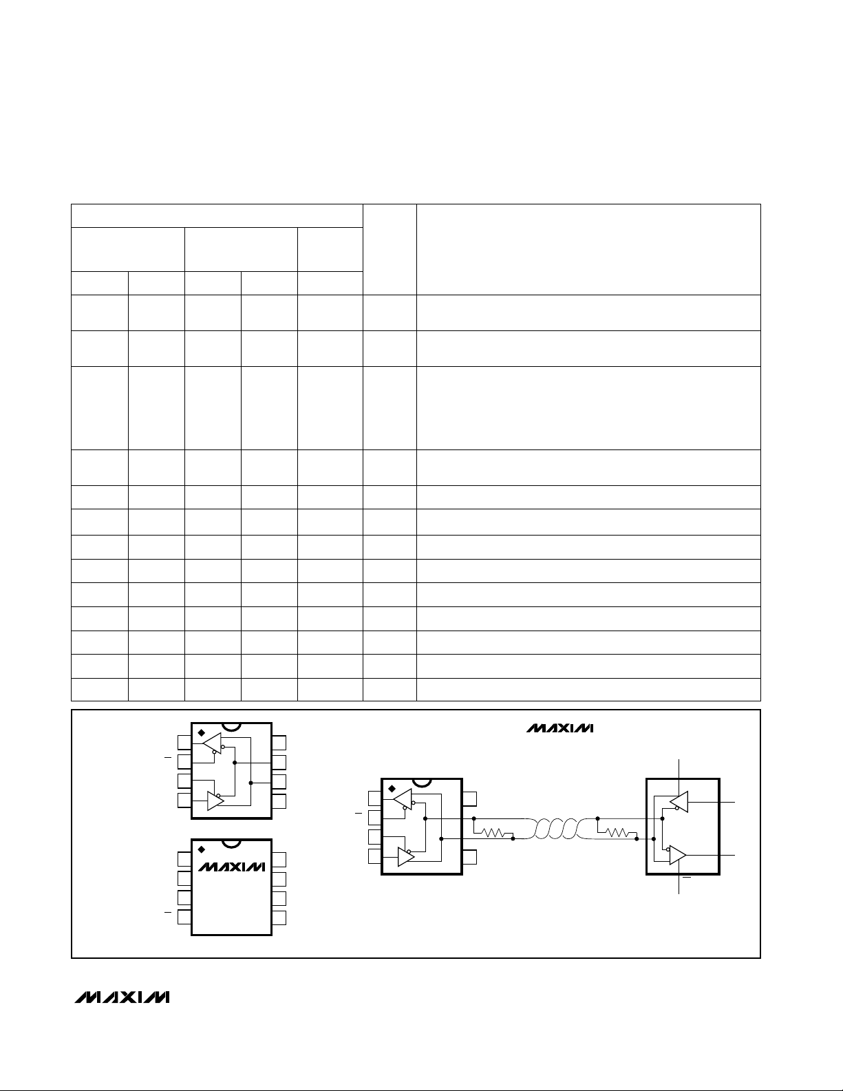
Figure 1. MAX481/MAX483/MAX485/MAX487/MAX1487 Pin Configuration and Typical Operating Circuit
DE
D
R
DI
RO
RE
_______________________________________________________________________________________ 7

Low-Power, Slew-Rate-Limited
RS-485/RS-422 Transceivers
TOP VIEW
V
GND
A
1
CC
RO
DI
R
2
3
4
D
8
B
7
6
Z
Y
5
3
DI
V
CC
1
5
DR
6
DIP/SO
2
B
1
A
2
MAX488
V
CC
RO
MAX490
3
4
8
Z
7
Y
6
GND
5
DI
RO
µMAX
4
GND
8
R
7
NOTE: TYPICAL OPERATING CIRCUIT SHOWN WITH DIP/SO PACKAGE.
Figure 2. MAX488/MAX490 Pin Configuration and Typical Operating Circuit
TOP VIEW
N.C.
RO
RE
DE
GND
GND
1
R
2
3
4
5
DI
6
7
D
14
13
12
11
10
9
8
V
CC
N.C.
A
B
Z
Y
N.C.
RO
NC
DI
1, 8, 13
DIP/SO
DE V
CC
144
5
D
2
3 6, 7
9
10
12
RD
11
RE GND
V
CC
MAX488
MAX490
Y
Z
A
Rt
B
Rt
D
GND
VCCRE
RO
DI
MAX489
MAX491
Y
Z
A
Rt
B
Rt
R
GND DE
RO
DI
Figure 3. MAX489/MAX491 Pin Configuration and Typical Operating Circuit
__________Applications Information
The MAX481/MAX483/MAX485/MAX487–MAX491 and
MAX1487 are low-power transceivers for RS-485 and RS422 communications. The MAX481, MAX485, MAX490,
MAX491, and MAX1487 can transmit and receive at data
rates up to 2.5Mbps, while the MAX483, MAX487,
MAX488, and MAX489 are specified for data rates up to
250kbps. The MAX488–MAX491 are full-duplex transceivers while the MAX481, MAX483, MAX485, MAX487,
and MAX1487 are half-duplex. In addition, Driver Enable
(DE) and Receiver Enable (RE) pins are included on the
The 48kΩ,
MAX487 and MAX1487 allows up to 128 transceivers
on a bus, compared to the 1-unit load (12kΩ input
impedance) of standard RS-485 drivers (32 transceivers maximum). Any combination of MAX487/
MAX1487 and other RS-485 transceivers with a total of
32 unit loads or less can be put on the bus. The
MAX481/MAX483/MAX485 and MAX488–MAX491 have
standard 12kΩ Receiver Input impedance.
1
/
-unit-load receiver input impedance of the
4
128 Transceivers on the Bus
MAX487/MAX1487:
MAX481, MAX483, MAX485, MAX487, MAX489,
MAX491, and MAX1487. When disabled, the driver and
MAX481/MAX483/MAX485/MAX487–MAX491/MAX1487
receiver outputs are high impedance.
8 _______________________________________________________________________________________

Low-Power, Slew-Rate-Limited
RS-485/RS-422 Transceivers
_________________________________________________________________Test Circuits
Y
R
V
OD
R
V
OC
Z
RECEIVER
OUTPUT
TEST POINT
C
RL
15pF
1k
Figure 4. Driver DC Test Load Figure 5. Receiver Timing Test Load
3V
DE
DI
Y
V
ID
Z
C
L1
R
DIFF
C
L2
A
RO
B
RE
OUTPUT
UNDER TEST
500Ω
C
L
S1
S2
1k
V
CC
V
S1
S2
CC
MAX481/MAX483/MAX485/MAX487–MAX491/MAX1487
Figure 6. Driver/Receiver Timing Test Circuit Figure 7. Driver Timing Test Load
MAX483/MAX487/MAX488/MAX489:
Reduced EMI and Reflections
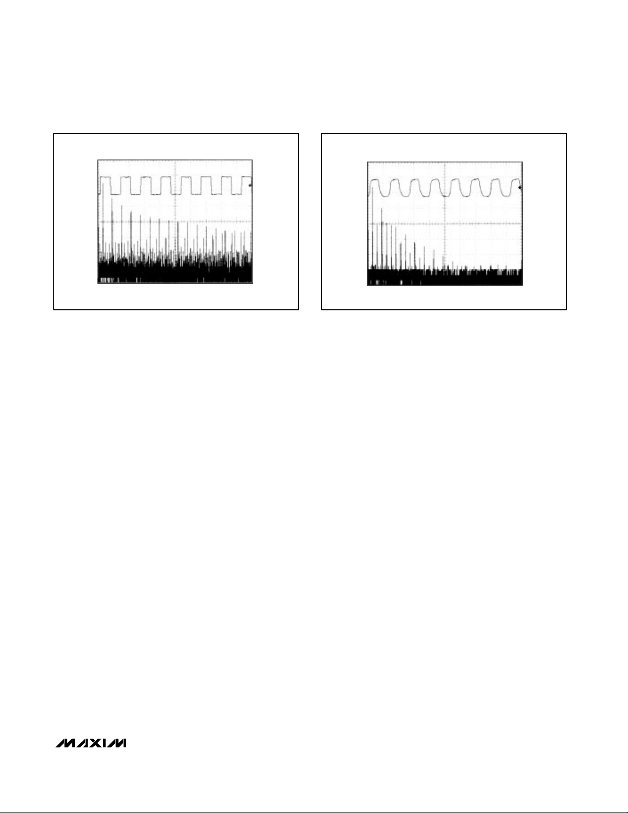
The MAX483 and MAX487–MAX489 are slew-rate limited, minimizing EMI and reducing reflections caused by
improperly terminated cables. Figure 12 shows the driver output waveform and its Fourier analysis of a
monics with large amplitudes are evident. Figure 13
shows the same information displayed for a MAX483,
MAX487, MAX488, or MAX489 transmitting under the
same conditions. Figure 13’s high-frequency harmonics
have much lower amplitudes, and the potential for EMI
is significantly reduced.
150kHz signal transmitted by a MAX481, MAX485,
MAX490, MAX491, or MAX1487. High-frequency har-
_______________________________________________________________________________________ 9

Low-Power, Slew-Rate-Limited
RS-485/RS-422 Transceivers
_______________________________________________________Switching Waveforms
3V
DI
V
DIFF
1.5V
0V
Z
V
O
Y
1/2 V
O
V
O
0V
-V
10%
O
t
R
t
90%
PLH
V
t
SKEW =
= V (Y) - V (Z)
DIFF
t
PHL
| t
- t
PLH
PHL
1.5V
1/2 V
O
90%
t
F
|
10%
3V
DE
Y, Z
V
Y, Z
1.5V 1.5V
0V
t
, t
ZL(SHDN)
ZL
2.3V
OL
0V
OUTPUT NORMALLY LOW
OUTPUT NORMALLY HIGH
2.3V
t
, t
ZH(SHDN)
ZH
t
LZ
V
+0.5V
OL
V
-0.5V
OH
t
HZ
Figure 8. Driver Propagation Delays Figure 9. Driver Enable and Disable Times (except MAX488 and
MAX490)
3V
RO
A-B
RE
0V
V
OH
V
OL
V
ID
-V
0V
ID
1.5V
OUTPUT
t
PHL
INPUT
t
1.5V
PLH
0V
V
CC
RO
RO
0V
1.5V 1.5V
t
, t
ZL(SHDN)
ZL
1.5V
OUTPUT NORMALLY LOW
OUTPUT NORMALLY HIGH
1.5V
t
, t
ZH(SHDN)
ZH
t
LZ
t
HZ
V
V
+ 0.5V
OL
OH
- 0.5V
Figure 10. Receiver Propagation Delays
Figure 11. Receiver Enable and Disable Times (except MAX488
and MAX490)
_________________Function Tables
(MAX481/MAX483/MAX485/MAX487/MAX1487)
Table 1. Transmitting Table 2. Receiving
INPUTS OUTPUTS
RE
X
X
0
1
X = Don't care
MAX481/MAX483/MAX485/MAX487–MAX491/MAX1487
High-Z = High impedance
Shutdown mode for MAX481/MAX483/MAX487
*
DE DI Z Y
1
1
0
0
1
0
X
X
0
1
High-Z
High-Z
High-Z
High-Z
*
1
0
*
RE DE A-B RO
0
0
0
1
X = Don't care
High-Z = High impedance
Shutdown mode for MAX481/MAX483/MAX487
*
10 ______________________________________________________________________________________
INPUTS OUTPUT
0
0
0
0
> +0.2V
< -0.2V
Inputs open
X
1
0
1
High-Z
*
Low-Power, Slew-Rate-Limited
RS-485/RS-422 Transceivers
MAX481/MAX483/MAX485/MAX487–MAX491/MAX1487
10dB/div
0Hz 5MHz
Figure 12. Driver Output Waveform and FFT Plot of MAX481/
MAX485/MAX490/MAX491/MAX1487 Transmitting a 150kHz
Signal
500kHz/div
Low-Power Shutdown Mode
(MAX481/MAX483/MAX487)
A low-power shutdown mode is initiated by bringing
both –R—E–high and DE low. The devices will not shut
down unless both the driver and receiver are disabled.
In shutdown, the devices typically draw only 0.1µA of
supply current.
–R—E–
and DE may be driven simultaneously; the parts are
guaranteed not to enter shutdown if –R—E–is high and DE
is low for less than 50ns. If the inputs are in this state
for at least 600ns, the parts are guaranteed to enter
shutdown.
For the MAX481, MAX483, and MAX487, the tZHand
tZLenable times assume the part was not in the lowpower shutdown state (the MAX485/MAX488–MAX491
and MAX1487 can not be shut down). The t
and t
ZL(SHDN)
down (see
It takes the drivers and receivers longer to become
enabled from the low-power shutdown state
(t
ZH(SHDN
(tZH, tZL). (The parts are in operating mode if the –R—E–,
DE inputs equal a logical 0,1 or 1,1 or 0, 0.)
enable times assume the parts were shut
Electrical Characteristics
), t
ZL(SHDN)
) than from the operating mode
).
ZH(SHDN)
10dB/div
0Hz 5MHz
Figure 13. Driver Output Waveform and FFT Plot of MAX483/
MAX487–MAX489 Transmitting a 150kHz Signal
500kHz/div
Driver Output Protection
Excessive output current and power dissipation caused
by faults or by bus contention are prevented by two
mechanisms. A foldback current limit on the output
stage provides immediate protection against short circuits over the whole common-mode voltage range (see
Typical Operating Characteristics
mal shutdown circuit forces the driver outputs into a
high-impedance state if the die temperature rises
excessively.
). In addition, a ther-
Propagation Delay
Many digital encoding schemes depend on the difference between the driver and receiver propagation
delay times. Typical propagation delays are shown in
Figures 15–18 using Figure 14’s test circuit.
The difference in receiver delay times, | t
typically under 13ns for the MAX481, MAX485,
MAX490, MAX491, and MAX1487 and is typically less
than 100ns for the MAX483 and MAX487–MAX489.
The driver skew times are typically 5ns (10ns max) for
the MAX481, MAX485, MAX490, MAX491, and
MAX1487, and are typically 100ns (800ns max) for the
MAX483 and MAX487–MAX489.
PLH
- t
PHL
|, is
______________________________________________________________________________________ 11

Low-Power, Slew-Rate-Limited
RS-485/RS-422 Transceivers
100pF
TTL IN
, tF < 6ns
t
R
Z
D
Y
R = 54Ω
100pF
Figure 14. Receiver Propagation Delay Test Circuit
B
R
A
RECEIVER
OUT
A
500mV/div
B
RO
2V/div
20ns/div
VCC = 5V
= +25°C
T
A
Figure 15. MAX481/MAX485/MAX490/MAX491/MAX1487
Receiver t
500mV/div
2V/div
RO
PHL
A
B
VCC = 5V
= +25°C
T
A
B
500mV/div
A
2V/div
RO
20ns/div
VCC = 5V
= +25°C
T
A
Figure 16. MAX481/MAX485/MAX490/MAX491/MAX1487
Receiver t
500mV/div
2V/div
PLH
B
VCC = 5V
= +25°C
T
A
A
RO
400ns/div
Figure 17. MAX483, MAX487–MAX489 Receiver t
MAX481/MAX483/MAX485/MAX487–MAX491/MAX1487
PHL
Figure 18. MAX483, MAX487–MAX489 Receiver t
400ns/div
PLH
12 ______________________________________________________________________________________
Low-Power, Slew-Rate-Limited
RS-485/RS-422 Transceivers
Line Length vs. Data Rate
The RS-485/RS-422 standard covers line lengths up to
4000 feet. For line lengths greater than 4000 feet, see
Figure 23.
Figures 19 and 20 show the system differential voltage
for the parts driving 4000 feet of 26AWG twisted-pair
wire at 110kHz into 120Ω loads.
Typical Applications
The MAX481, MAX483, MAX485, MAX487–MAX491, and
MAX1487 transceivers are designed for bidirectional data
communications on multipoint bus transmission lines.
DI
V
Y-VZ
RO
5V
0V
1V
0V
-1V
5V
0V
Figures 21 and 22 show typical network applications
circuits. These parts can also be used as line
repeaters, with cable lengths longer than 4000 feet, as
shown in Figure 23.
To minimize reflections, the line should be terminated at
both ends in its characteristic impedance, and stub
lengths off the main line should be kept as short as possible. The slew-rate-limited MAX483 and MAX487–MAX489
are more tolerant of imperfect termination.
5V
0V
1V
0V
-1V
5V
0V
V
DI
Y-VZ
RO
MAX481/MAX483/MAX485/MAX487–MAX491/MAX1487
2µs/div
Figure 19. MAX481/MAX485/MAX490/MAX491/MAX1487
System Differential Voltage at 110kHz Driving 4000ft of Cable
120Ω
DI
D
DE
RO
RE
R
MAX481
B
A
B
A
D
R
Figure 20. MAX483, MAX487–MAX489 System Differential
Voltage at 110kHz Driving 4000ft of Cable
120Ω
B
A
R
D
MAX483
MAX485
MAX487
DI RO DE
DE
DI
RO
RERE
MAX1487
Figure 21. MAX481/MAX483/MAX485/MAX487/MAX1487 Typical Half-Duplex RS-485 Network
______________________________________________________________________________________ 13
2µs/div
B
A
DE
D
DI
R
RO
RE
Low-Power, Slew-Rate-Limited
RS-485/RS-422 Transceivers
A
RO
RE
DE
DI
R
D
120Ω
B
Z
120Ω
Y
Z
Y
AA
BB
R
D
DI DIRO RO
DE DE
RE
NOTE: RE AND DE ON MAX489/MAX491 ONLY.
Figure 22. MAX488–MAX491 Full-Duplex RS-485 Network
MAX488–MAX491
Y
120Ω
Z
B
120Ω
Z
Y
A
D
R
DI
DE
RE
RO
R
D
MAX488
MAX489
MAX490
RE
MAX491
Isolated RS-485
For isolated RS-485 applications, see the MAX253 and
MAX1480 data sheets.
A
RO
RE
DE
DI
R
D
120Ω
B
Z
120Ω
Y
DATA IN
DATA OUT
NOTE: RE AND DE ON MAX489/MAX491 ONLY.
Figure 23. Line Repeater for MAX488–MAX491
MAX481/MAX483/MAX485/MAX487–MAX491/MAX1487
14 ______________________________________________________________________________________

Low-Power, Slew-Rate-Limited
RS-485/RS-422 Transceivers
__Ordering Information (continued)
PIN-PACKAGETEMP. RANGEPART
8 Plastic DIP-40°C to +85°CMAX481EPA
8 SO-40°C to +85°CMAX481ESA
8 CERDIP-55°C to +125°CMAX481MJA
MAX483CPA
MAX485CPA
MAX487CPA
MAX488CPA
MAX489CPD
8 Plastic DIP0°C to +70°C
8 SO0°C to +70°CMAX483CSA
8 µMAX0°C to +70°CMAX483CUA
Dice*0°C to +70°CMAX483C/D
8 Plastic DIP-40°C to +85°CMAX483EPA
8 SO-40°C to +85°CMAX483ESA
8 CERDIP-55°C to +125°CMAX483MJA
8 Plastic DIP0°C to +70°C
8 SO0°C to +70°CMAX485CSA
8 µMAX0°C to +70°CMAX485CUA
Dice*0°C to +70°CMAX485C/D
8 Plastic DIP-40°C to +85°CMAX485EPA
8 SO-40°C to +85°CMAX485ESA
8 CERDIP-55°C to +125°CMAX485MJA
8 Plastic DIP0°C to +70°C
8 SO0°C to +70°CMAX487CSA
8 µMAX0°C to +70°CMAX487CUA
Dice*0°C to +70°CMAX487C/D
8 Plastic DIP-40°C to +85°CMAX487EPA
8 SO-40°C to +85°CMAX487ESA
8 CERDIP-55°C to +125°CMAX487MJA
8 Plastic DIP0°C to +70°C
8 SO0°C to +70°CMAX488CSA
8 µMAX0°C to +70°CMAX488CUA
Dice*0°C to +70°CMAX488C/D
8 Plastic DIP-40°C to +85°CMAX488EPA
8 SO-40°C to +85°CMAX488ESA
8 CERDIP-55°C to +125°CMAX488MJA
14 Plastic DIP0°C to +70°C
14 SO0°C to +70°CMAX489CSD
Dice*0°C to +70°CMAX489C/D
14 Plastic DIP-40°C to +85°CMAX489EPD
14 SO-40°C to +85°CMAX489ESD
14 CERDIP-55°C to +125°CMAX489MJD
__Ordering Information (continued)
PIN-PACKAGETEMP. RANGEPART
MAX490CPA
MAX491CPD
MAX1487CPA
* Contact factory for dice specifications.
8 Plastic DIP0°C to +70°C
8 SO0°C to +70°CMAX490CSA
8 µMAX0°C to +70°CMAX490CUA
Dice*0°C to +70°CMAX490C/D
8 Plastic DIP-40°C to +85°CMAX490EPA
8 SO-40°C to +85°CMAX490ESA
8 CERDIP-55°C to +125°CMAX490MJA
14 Plastic DIP0°C to +70°C
14 SO0°C to +70°CMAX491CSD
Dice*0°C to +70°CMAX491C/D
14 Plastic DIP-40°C to +85°CMAX491EPD
14 SO-40°C to +85°CMAX491ESD
14 CERDIP-55°C to +125°CMAX491MJD
8 Plastic DIP0°C to +70°C
8 SO0°C to +70°CMAX1487CSA
8 µMAX0°C to +70°CMAX1487CUA
Dice*0°C to +70°CMAX1487C/D
8 Plastic DIP-40°C to +85°CMAX1487EPA
8 SO-40°C to +85°CMAX1487ESA
8 CERDIP-55°C to +125°CMAX1487MJA
_________________Chip Topographies
MAX481/MAX483/MAX485/MAX487/MAX1487
V
CC
RO
RE
DE
DI
GND
0.080"
(2.032mm)
N.C.
N.C.
0.054"
B
(1.372mm)
A
MAX481/MAX483/MAX485/MAX487–MAX491/MAX1487
______________________________________________________________________________________ 15
Low-Power, Slew-Rate-Limited
RS-485/RS-422 Transceivers
_____________________________________________Chip Topographies (continued)
MAX489/MAX491
V
CC
GND
0.080"
(2.032mm)
A
B
0.054"
Z
(1.372mm)
Y
N.C.
N.C.
RO
DI
MAX488/MAX490
V
CC
GND
0.080"
(2.032mm)
A
B
0.054"
Z
(1.372mm)
Y
RO
RE
DE
DI
TRANSISTOR COUNT: 248
SUBSTRATE CONNECTED TO GND
________________________________________________________Package Information
DIM
C
A
0.101mm
e
A1B
0.004 in
L
α
A
A1
B
C
D
E
H
INCHES MILLIMETERS
MIN
0.036
0.004
0.010
0.005
0.116
0.116
e
0.188
L
0.016
α
MAX
0.044
0.008
0.014
0.007
0.120
0.120
0°
0.198
0.026
6°
MIN
0.91
0.10
0.25
0.13
2.95
2.95
4.78
0.41
0°
MAX
1.11
0.20
0.36
0.18
3.05
3.05
0.650.0256
5.03
0.66
6°
21-0036D
E H
8-PIN µMAX
MICROMAX SMALL-OUTLINE
PACKAGE
D
MAX481/MAX483/MAX485/MAX487–MAX491/MAX1487
Maxim cannot assume responsibility for use of any circuitry other than circuitry entirely embodied in a Maxim product. No circuit patent licenses are
implied. Maxim reserves the right to change the circuitry and specifications without notice at any time.
16
__________________Maxim Integrated Products, 120 San Gabriel Drive, Sunnyvale, CA 94086 (408) 737-7600
© 1996 Maxim Integrated Products Printed USA is a registered trademark of Maxim Integrated Products.
 Loading...