

For free samples & the latest literature: http://www.maxim-ic.com, or phone 1-800-998-8800.
For small orders, phone 408-737-7600 ext. 3468.
_______________General Description
The MAX1481/MAX1484/MAX1485/MAX1486 provide
software-selectable, half-/full-duplex, low-power, slewrate-limited, and high-speed (12Mbps) RS-485/RS-422
operation in a 10-pin µMAX® package—the smallest 10-pin package available.
The software-selectable, half-/full-duplex MAX1485/
MAX1486 make obsolete the normally larger and more
expensive solutions required for selectable half-/fullduplex RS-485/RS-422 operation: 1) a 14-pin, fullduplex transceiver configured via jumpers between
receiver and transmitter lines, or 2) two 8-pin, halfduplex transceivers, which require an additional inverter logic gate for software selectability.
The MAX1481/MAX1484 are functionally equivalent to
the industry-standard MAX491 and 75180, and are
designed for space-constrained, full-duplex RS-422
applications.
All parts contain one driver and one receiver and feature a 1/8-unit-load receiver input impedance, allowing
up to 256 transceivers on the bus. The MAX1481/
MAX1485 feature reduced-slew-rate drivers that minimize EMI and reduce reflections caused by improperly
terminated cables, allowing error-free data transmission
up to 250kbps. The MAX1484/MAX1486 driver slew
rates are not limited, allowing them to transmit up to
12Mbps.
The MAX1481/MAX1484/MAX1485/MAX1486 draw only
300µA of supply current. The MAX1481 has a low-power
shutdown mode that reduces supply current to only
0.1µA. All devices operate from a single 5V supply.
Drivers are output short-circuit current limited and are
protected against excessive power dissipation by
thermal-shutdown circuitry that places the driver outputs
into a high-impedance state. The receiver input has a failsafe feature that guarantees a logic-high output if the
input is open circuit.
____________________________Features
♦ 10-Pin µMAX Package: Smallest 10-Pin Package
♦ Software-Selectable Half-/Full-Duplex Operation
(MAX1485/MAX1486)
♦ 0.1µA Low-Current Shutdown Mode (MAX1481)
♦ Slew-Rate Limiting Allows Error-Free Data
Transmission (MAX1481/MAX1485)
♦ 12Mbps High-Speed Operation
(MAX1484/MAX1486)
♦ Allow up to 256 Transceivers on the Bus
________________________Applications
Low-Power RS-422/RS-485 Communications
Level Translators
Hand-Held Equipment
Battery-Powered Equipment
Transceiver for EMI-Sensitive Applications
Industrial-Control Local Area Networks
MAX1481/MAX1484/MAX1485/MAX1486
Software-Selectable, Half-/Full-Duplex, Slew-Rate-Limited,
12Mbps, RS-485/RS-422 Transceivers in µMAX Package
________________________________________________________________
Maxim Integrated Products
1
19-1312; Rev 1; 3/06
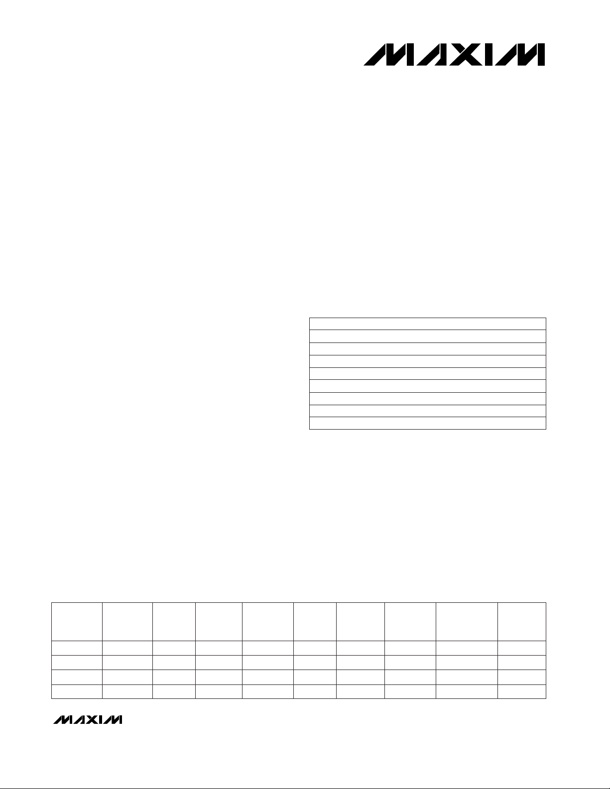
PART
MAX1481CUB
MAX1481EUB
MAX1484CUB
0°C to +70°C
-40°C to +85°C
0°C to +70°C
TEMP RANGE PIN-PACKAGE
10 µMAX
10 µMAX
10 µMAX
______________Ordering Information
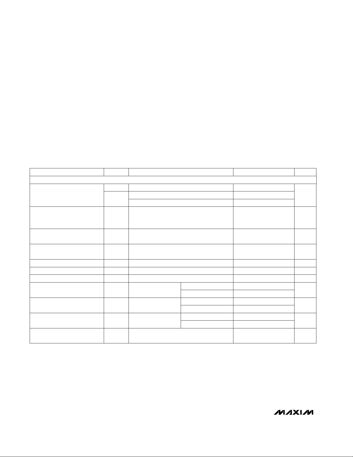
______________________________________________________________Selection Table
Half/Full
Duplex
Data
Rate
(Mbps)
MAX1481 Full 0.250
MAX1484 Full 12
Part
MAX1485 Selectable 0.250
MAX1486 Selectable 12
Slew-
Rate
Limited
Yes
No
Yes
No
Low-
Power
Shutdown
Driver
Enable
Yes Yes
No Yes
No Yes
No Yes
Quiescent
Current
(µA)
300
300
300
300
Transceivers
on Bus
256
256
256
256
Pin-
Package
10 µMAX
10 µMAX
10 µMAX
10 µMAX
MAX1484EUB -40°C to +85°C 10 µMAX
Receiver
Enable
Yes
Yes
No
No
MAX1485CUB
MAX1485EUB
MAX1486CUB
0°C to +70°C
-40°C to +85°C
0°C to +70°C 10 µMAX
10 µMAX
10 µMAX
MAX1486EUB -40°C to +85°C 10 µMAX
________________________________________________________________ Maxim Integrated Products 1
For pricing, delivery, and ordering information, please contact Maxim/Dallas Direct! at
1-888-629-4642, or visit Maxim’s website at www.maxim-ic.com.
µMAX is a registered trademark of Maxim Integrated Products, Inc.
MAX1481/MAX1484/MAX1485/MAX1486
Software-Selectable, Half-/Full-Duplex, Slew-Rate-Limited,
12Mbps, RS-485/RS-422 Transceivers in µMAX Package
2 _______________________________________________________________________________________
ABSOLUTE MAXIMUM RATINGS
ELECTRICAL CHARACTERISTICS
(VCC= +5V ±5%, TA= T
MIN
to T
MAX
, unless otherwise noted. Typical values are at VCC= +5V and TA= +25°C.) (Note 1)
Stresses beyond those listed under “Absolute Maximum Ratings” may cause permanent damage to the device. These are stress ratings only, and functional
operation of the device at these or any other conditions beyond those indicated in the operational sections of the specifications is not implied. Exposure to
absolute maximum rating conditions for extended periods may affect device reliability.
Supply Voltage (VCC) ............................................................+7V
Control Input Voltage (
RE, DE, H/F)...........-0.3V to (VCC+ 0.3V)
Driver Input Voltage (DI).............................-0.3V to (V
CC
+ 0.3V)
Driver Output Voltage (A, B, Y, Z)..........................-8V to +12.5V
Receiver Input Voltage, Half Duplex (Y, Z) ............-8V to +12.5V
Receiver Input Voltage, Full Duplex (A, B).............-8V to +12.5V
Receiver Output Voltage (RO)....................-0.3V to (V
CC
+ 0.3V)
Continuous Power Dissipation
10-Pin µMAX (derate 5.6mW/°C above +70°C)............444mW
Operating Temperature Ranges
MAX148_C_ _ ......................................................0°C to +70°C
MAX148_E_ _....................................................-40°C to +85°C
Storage Temperature Range.............................-65°C to +160°C
Lead Temperature (soldering, 10sec).............................+300°C
R = 50Ω (RS-422), Figure 5
No load, Figure 5
-7V ≤ V
OUT
≤ 12V
DE = GND
DE, DI, RE, H/F
DE, DI, RE, H/F
R = 50Ω or 27Ω, Figure 5
R = 50Ω or 27Ω, Figure 5
R = 50Ω or 27Ω, Figure 5
DE = GND,
VCC= GND or 5.25V
DE, DI, RE, H/F
CONDITIONS
mA35 250I
OSD
Driver Output Short-Circuit
Current (Note 3)
µA
-10
I
O
10
Output Leakage (Y and Z)
(MAX1481/MAX1484 Only)
mA
0.125
I
IN2
Input Current (Y and Z for Half
Duplex, A and B for Full Duplex)
µA±2I
IN1
Input Current
2.0
V
OD1
Differential Driver Output
5
V0.8V
IL1
Input Low Voltage
V2.0V
IH1
Input High Voltage
V0.2∆V
OC
Change in Magnitude of
Common-Mode Voltage (Note 2)
V0.2∆V
OD
Change in Magnitude of
Differential Output Voltage
(Note 2)
V3V
OC
Driver Common-Mode Output
Voltage
UNITSMIN TYP MAXSYMBOLPARAMETER
DE = GND
-100
I
O
µA
125
Output Leakage (Y and Z)
(MAX1485/MAX1486 Only)
V
OD2
R = 27Ω (RS-485), Figure 5
V
1.5 5
VIN= 12V
VIN= -7V
VIN= 12V
VIN= -7V
VIN= 12V
VIN= -7V
-0.1
DRIVER
Driver Input to Output
MAX1481/MAX1484/MAX1485/MAX1486
Software-Selectable, Half-/Full-Duplex, Slew-Rate-Limited,
12Mbps, RS-485/RS-422 Transceivers in µMAX Package
_______________________________________________________________________________________ 3
ELECTRICAL CHARACTERISTICS (continued)
(V
CC
= +5V ±5%, TA = T
MIN
to T
MAX
, unless otherwise noted. Typical values are at V
CC
= +5V and TA = +25°C.) (Note 1)
SWITCHING CHARACTERISTICS (MAX1484/MAX1486)
(V
CC
= 5V ±5%, TA = T
MIN
to T
MAX
, unless otherwise noted. Typical values are at V
CC
= +5V and TA = +25°C.)
-7V ≤ VCM≤ 12V
-7V ≤ VCM≤ 12V
IO= 4mA, VID= -200mV
IO= -4mA, VID= 200mV
0.4V ≤ VO≤ 2.4V
CONDITIONS
kΩ96R
IN
Receiver Input Resistance
µA±1I
OZR
Three-State Output Current at
Receiver
mV70∆V
TH
Receiver Input Hysteresis
mV-200 200V
TH
Receiver Differential Threshold
Voltage
V0.4V
OL
Receiver Output Low Voltage
V3.5V
OH
Receiver Output High Voltage
UNITSMIN TYP MAXSYMBOLPARAMETER
0V ≤ VRO≤ V
CC
RE = GND, DE = V
CC
mA±95I
OSR
Receiver Output Short-Circuit
Current
µA300 600I
CC
No-Load Supply Current
DE = GND, RE = V
CC
µA0.1 10I
SHDN
Supply Current in Shutdown
Mode (MAX1481 Only)
R
DIFF
= 54Ω, CL1= CL2= 100pF,
Figures 7 and 9
R
DIFF
= 54Ω, CL1= CL2= 100pF,
Figures 7 and 9
CONDITIONS
ns5 10t
DSKEW
Driver Output Skew
| t
DPLH
- t
DPHL
|
30 60t
DPLH
ns
30 60t
DPHL
Driver Input to Output
UNITSMIN TYP MAXSYMBOLPARAMETER
CL= 15pF, S1 closed, Figures 8 and 10
CL= 100pF, S2 closed, Figures 8 and 10
CL= 100pF, S1 closed, Figures 8 and 10
ns40 70t
DLZ
Driver Disable Time from Low
ns40 70t
DZH
Driver Enable to Output High
ns40 70t
DZL
Driver Enable to Output Low
Mbps12f
MAX
Maximum Data Rate
CL= 15pF, S2 closed, Figures 8 and 10
CL= 100pF, S2 closed, Figures 6 and 12
CL= 100pF, S1 closed, Figures 6 and 12
ns20 50t
RZH
Receiver Enable to Output High
ns20 50t
RZL
Receiver Enable to Output Low
ns40 70t
DHZ
Driver Disable Time from High
CL= 100pF, S2 closed, Figures 6 and 12
CL= 100pF, S1 closed, Figures 6 and 12
ns20 50t
RHZ
Receiver Disable Time from High
ns20 50t
RLZ
Receiver Disable Time from Low
Figures 11 and 13 ns5t
RSKD
| t
RPLH
- t
RPHL
| Differential
Receiver Skew
Figures 11 and 13 ns90 150
t
RPLH
,
t
RPHL
Receiver Input to Output
R
DIFF
= 54Ω, CL1= CL2= 100pF,
Figures 7 and 9
ns5 15 35tDR, t
DF
Driver Rise or Fall Time
RECEIVER
SUPPLY CURRENT
MAX1481/MAX1484/MAX1485/MAX1486
Software-Selectable, Half-/Full-Duplex, Slew-Rate-Limited,
12Mbps, RS-485/RS-422 Transceivers in µMAX Package
4 _______________________________________________________________________________________
SWITCHING CHARACTERISTICS (MAX1481/MAX1485) (continued)
(VCC= 5V ±5%, TA= T
MIN
to T
MAX
, unless otherwise noted. Typical values are at VCC= +5V and TA= +25°C.)
Note 1: All currents into the device are positive; all currents out of the device are negative. All voltages are referenced to device
ground unless otherwise noted.
Note 2: ∆V
OD
and ∆VOCare the changes in VODand VOC, respectively, when the DI input changes state.
Note 3: Maximum current level applies to peak current just prior to foldback-current limiting; minimum current level applies during
current limiting.
Note 4: Shutdown is enabled by bringing RE high and DE low. If the enable inputs are in this state for less than 50ns, the MAX1481
is guaranteed not to enter shutdown. If the enable inputs are in this state for at least 600ns, the MAX1481 is guaranteed to
have entered shutdown.
CL= 15pF, S1 closed, Figures 8 and 10
CL= 100pF, S2 closed, Figures 8 and 10
R
DIFF
= 54Ω, CL1= CL2= 100pF,
Figures 7 and 9
CL= 100pF, S1 closed, Figures 8 and 10
R
DIFF
= 54Ω, CL1= CL2= 100pF,
Figures 7 and 9
ns200t
DLZ
CL= 100pF, S2 closed, Figures 6 and 12
Driver Disable Time from Low
CL= 100pF, S1 closed, Figures 6 and 12
R
DIFF
= 54Ω, CL1= CL2= 100pF,
Figures 7 and 9
ns3000t
DZH
Driver Enable to Output High
ns3000
CONDITIONS
t
DZL
Driver Enable to Output Low
kbps250f
MAX
Maximum Data Rate
CL= 15pF, S2 closed, Figures 8 and 10
CL= 100pF, S2 closed, Figures 6 and 12
CL= 100pF, S1 closed, Figures 6 and 12
ns10 200t
DSKEW
Driver Output Skew
| t
DPLH
- t
DPHL
|
Figures 11 and 13
ns
ns20 50t
RZH
Receiver Enable to Output High
ns20 50t
RZL
Receiver Enable to Output Low
ns200t
DHZ
Driver Disable Time from High
ns
ns20 50t
RHZ
Receiver Disable Time from High
90 150
t
RPLH
,
t
RPHL
Receiver Input to Output
250 1000tDR, t
DF
Driver Rise or Fall Time
ns20 50t
RLZ
Receiver Disable Time from Low
Figures 11 and 13 ns15t
RSKD
| t
RPLH
- t
RPHL
| Differential
Receiver Skew
600 1000t
DPLH
ns
600 1000t
DPHL
Driver Input to Output
UNITSMIN TYP MAXSYMBOLPARAMETER
MAX1481 only (Note 4) ns50 200 600t
SHDN
Time to Shutdown
MAX1481 only, CL= 15pF, S2 closed,
Figures 8 and 10
ns3000t
DZH(SHDN)
Driver Enable from Shutdown to
Output High
MAX1481 only, CL= 15pF, S1 closed,
Figures 8 and 10
ns3000t
DZL(SHDN)
Driver Enable from Shutdown to
Output Low
MAX1481 only, CL= 100pF, S1 closed,
Figures 6 and 12
ns1000t
RZL(SHDN)
Receiver Enable from Shutdown
to Output Low
MAX1481 only, CL= 100pF, S2 closed,
Figures 6 and 12
ns500t
RZH(SHDN)
Receiver Enable from Shutdown
to Output High
MAX1481/MAX1484/MAX1485/MAX1486
Software-Selectable, Half-/Full-Duplex, Slew-Rate-Limited,
12Mbps, RS-485/RS-422 Transceivers in µMAX Package
_______________________________________________________________________________________
5
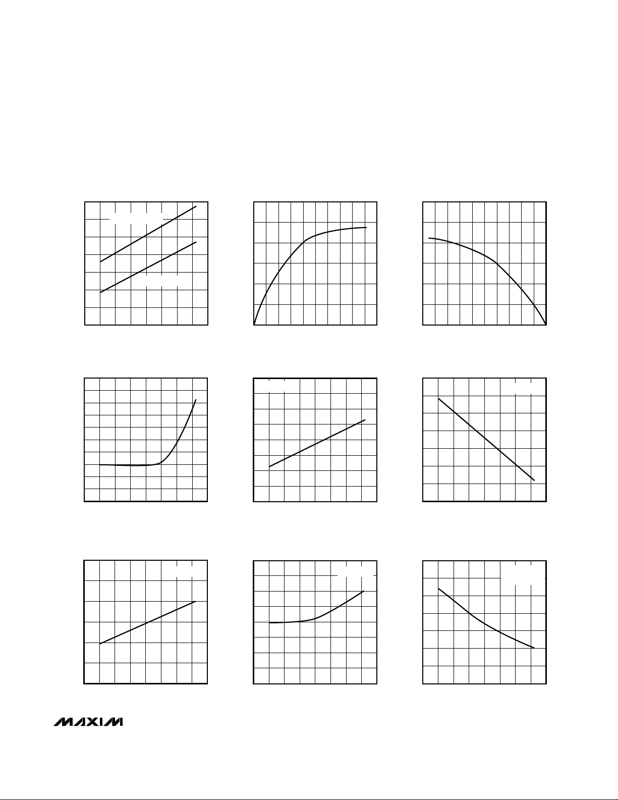
220
260
240
300
280
340
320
360
-60 -20 0-40 20 40 60 80 100
NO-LOAD SUPPLY CURRENT
vs. TEMPERATURE
MAX1481/4/5/6-01
TEMPERATURE (°C)
SUPPLY CURRENT (µA)
MAX1481/MAX1485
MAX1484/MAX1486
0
10
30
20
50
40
60
0
1
2 3 4 5
OUTPUT CURRENT vs.
RECEIVER OUTPUT LOW VOLTAGE
MAX1481/4/5/6-02
OUTPUT LOW VOLTAGE (V)
OUTPUT CURRENT (mA)
0
5
15
10
25
20
30
0
1
2 3 4 5
OUTPUT CURRENT vs.
RECEIVER OUTPUT HIGH VOLTAGE
MAX1481/4/5/6-03
OUTPUT LOW VOLTAGE (V)
OUTPUT CURRENT (mA)
94
98
106
102
110
114
-60 -20 0-40 20 40 60 80 100
SHUTDOWN CURRENT
vs. TEMPERATURE
MAX1481/4/5/6-04
TEMPERATURE (°C)
SHUTDOWN CURRENT (nA)
75
80
90
85
100
95
105
-60 -20 0-40 20 40 60 80 100
MAX1481/MAX1485 RECEIVER
PROPAGATION DELAY vs. TEMPERATURE
MAX1481/4/5/6-07
TEMPERATURE (°C)
PROPAGATION DELAY (ns)
C
LOAD
= 15pF
0.10
0.20
0.15
0.35
0.30
0.25
0.45
0.40
0.50
-60 -20 0-40 20 40 60 80 100
RECEIVER OUTPUT LOW VOLTAGE
vs. TEMPERATURE
MAX1481/4/5/6-05
TEMPERATURE (°C)
OUTPUT LOW VOLTAGE (V)
IRO = 8mA
3.8
4.0
3.9
4.2
4.1
4.4
4.3
4.5
-60 -20 0-40 20 40 60 80 100
RECEIVER OUTPUT HIGH VOLTAGE
vs. TEMPERATURE
MAX1481/4/5/6-06
TEMPERATURE (°C)
OUTPUT VOLTAGE (V)
IRO = 8mA
86
87
90
89
88
93
92
91
94
-60 -20 0-40 20 40 60 80 100
MAX1484/MAX1486 RECEIVER
PROPAGATION DELAY vs. TEMPERATURE
MAX1481/4/5/6-08
TEMPERATURE (°C)
PROPAGATION DELAY (ns)
C
LOAD
= 15pF
540
580
560
620
600
660
640
680
-60 -20 0-40 20 40 60 80 100
MAX1481/MAX1485 DRIVER
PROPAGATION DELAY vs. TEMPERATURE
MAX1481/4/5/6-09
TEMPERATURE (°C)
PROPAGATION DELAY (ns)
R
DIFF
= 54Ω
C
L1 = CL2 = 100pF
__________________________________________Typical Operating Characteristics
(VCC= +5V, TA= +25°C, unless otherwise noted.)

MAX1481/MAX1484/MAX1485/MAX1486
Software-Selectable, Half-/Full-Duplex, Slew-Rate-Limited,
12Mbps, RS-485/RS-422 Transceivers in µMAX Package
6 _______________________________________________________________________________________
_________________________________Typical Operating Characteristics (continued)
(VCC= +5V, TA= +25°C, unless otherwise noted.)
18
26
22
30
34
38
-60 -20 0-40 20 40 60 80 100
MAX1484/MAX1486 DRIVER
PROPAGATION DELAY vs. TEMPERATURE
MAX1481/4/5/6-10
TEMPERATURE (°C)
PROPAGATION DELAY (ns)
R
DIFF
= 54Ω
C
L1 = CL2 = 100pF
0
60
40
20
80
120
100
140
0 42 6 8 10 12
OUTPUT CURRENT vs.
DRIVER OUTPUT LOW VOLTAGE
MAX1481/4/5/6-11
OUTPUT LOW VOLTAGE (V)
OUTPUT CURRENT (mA)
0
40
20
60
100
80
120
-8 -4 -2-6 0 2 4 6
OUTPUT CURRENT vs.
DRIVER OUTPUT HIGH VOLTAGE
MAX1481/4/5/6-12
OUTPUT HIGH VOLTAGE (V)
OUTPUT CURRENT (mA)
2.10
2.15
2.25
2.20
2.35
2.30
2.40
-60 -20 0-40 20 40 60 80 100
DRIVER DIFFERENTIAL OUTPUT
VOLTAGE vs. TEMPERATURE
MAX1481/4/5/6-13
TEMPERATURE (°C)
OUTPUT VOLTAGE (V)
R
DIFF
= 54Ω
VA - V
B
RO
(2V/div)
(5V/div)
1µs/div
MAX1481/MAX1485
RECEIVER PROPAGATION DELAY
MAX1481/4/5/6-16
100
0.01
0 2.5 3.0 3.5 4.0 4.50.5 1.0 1.5 2.0 5.0
DRIVER OUTPUT CURRENT
vs. DIFFERENTIAL OUTPUT VOLTAGE
0.1
MAX1481/4/5/6-14
DIFFERENTIAL OUTPUT VOLTAGE (V)
OUTPUT CURRENT (mA)
1
10
VA - V
B
RO
(2V/div)
(5V/div)
50ns/div
MAX1484/MAX1486
RECEIVER PROPAGATION DELAY
MAX1481/4/5/6-15
DI
V
Y
- V
Z
(5V/div)
(2V/div)
1µs/div
MAX1481/MAX1485
DRIVER PROPAGATION DELAY
MAX1481/4/5/6-17
DI
V
Y
- V
Z
5V/div
2V/div
50ns/div
MAX1484/MAX1486
DRIVER PROPAGATION DELAY
MAX1481/4/5/6-18

PIN
MAX1481/MAX1484/MAX1485/MAX1486
Software-Selectable, Half-/Full-Duplex, Slew-Rate-Limited,
12Mbps, RS-485/RS-422 Transceivers in µMAX Package
_______________________________________________________________________________________ 7
______________________________________________________________Pin Description
1 1
Receiver Output. When RE is low and if A - B ≥ 200mV, RO goes high; if A - B ≤
-200mV, RO goes low.
— 2
Half-/Full-Duplex Selector Input. Connect H/F to VCCfor half-duplex mode, and
connect to GND for full-duplex mode.
2 —
Receiver Output Enable Input. Drive RE low to enable RO; RO is high impedance
when RE is high. For MAX1481 only, drive RE high and DE low to enter the lowpower shutdown mode.
3 3
Driver Output Enable Input. Drive DE high to enable driver outputs. These outputs
are high impedance when DE is low.
4 4
Driver Input. With DE high, a low on DI forces noninverting output low and inverting output high. Similarly, a high on DI forces noninverting output high and invert-
ing output low.
5 5 Ground
6 6 Inverting Receiver Input
— — Receiver Input Resistors*
7 7 Inverting Driver Output
— — Inverting Driver Output and Inverting Receiver Input
8 8 Noninverting Driver Output
— — Noninverting Driver Output and Noninverting Receiver Input
9 9 Noninverting Receiver Input
— — Receiver Input Resistors*
10 10 Positive Supply; +4.75V ≤ VCC≤ +5.25V
MAX1481/
MAX1484
1 RO
2
H/F
PIN
—
RE
3 DE
4 DI
5 GND
— B
6 B
— Z
7 Z
— Y
8 Y
— A
9 A
10 V
CC
MAX1485/MAX1486
H/F = 0
FUNCTIONNAME
H/F = 1
*
(MAX1485/MAX1486 only) In half-duplex mode, the driver outputs serve as receiver inputs. The full-duplex receiver inputs (A and B)
will still have a 1/8-unit load, but are not connected to the receiver.

OUTPUT
INPUTS
MAX1481/MAX1484/MAX1485/MAX1486
Software-Selectable, Half-/Full-Duplex, Slew-Rate-Limited,
12Mbps, RS-485/RS-422 Transceivers in µMAX Package
8 _______________________________________________________________________________________
RE
DE
X 1
X 1
0 0
1 0
DI Z
1 0
0 1
X High-Z
X
INPUTS
_____________________________________________________________Function Tables
TRANSMITTING
Y
1
0
High-Z
High-Z and Shutdown
OUTPUTS
MAX1481
MAX1484
MAX1485/MAX1486
RE
DE
0 X
0 X
1 1
1 0
High-Z and
Shutdown
OUTPUT
A-B RO
≥ 0.2V 1
≤ -0.2V 0
X High-Z
X
INPUTS
RECEIVING
TRANSMITTING
RE
DE Y
X 1 1
X 1 0
X 0 High-Z
OUTPUTS
DI Z
1 0
0 1
X High-Z
INPUTS
RE
DE
0 X
0 X
1 X
OUTPUT
A-B RO
≥ 0.2V 1
≤ -0.2V 0
X High-Z
INPUTS
RECEIVING
DE DI
TRANSMITTING
1 1
1 0
0 X
Z Y
0 1
1 0
High-Z High-Z
OUTPUTS
RECEIVING
H/F
DE RO
0 X 1
0 X 0
1 0 1
OUTPUT
A-B Y-Z
≥ 0.2V X
≤ -0.2V X
X ≥ 0.2V
INPUTS
1 0 0X ≤ -0.2V
X = Don’t care
Note: In shutdown mode, driver and receiver outputs are high impedance.
INPUTS

MAX1481/MAX1484/MAX1485/MAX1486
Software-Selectable, Half-/Full-Duplex, Slew-Rate-Limited,
12Mbps, RS-485/RS-422 Transceivers in µMAX Package
_______________________________________________________________________________________ 9
1
2
3
4
5
1
9 A
R
t
R
t
10
0.1µF
5
GND
6 B
Z
7
8
Y
RO
RE
DE
DI
2
3
4
10
9
8
7
6
V
CC
A
Y
ZDI
DE
RE
RO
MAX1481
MAX1484
MAX1481
MAX1484
MAX1481
MAX1484
µMAX
TOP VIEW
BGND
8
4
10
0.1µF
5
GND
3
2
DI
DE
RE
RO
1
Y
Z
B
A
7
6
9
V
CC
V
CC
Figure 1. MAX1481/MAX1484 Pin Configuration and Typical Full-Duplex Operating Circuit
1
2
3
4
5
1
9 A
R
t
R
t
10
0.1µF
V
CC
5
GND
6 B
Z
7
8
Y
RO
H/F
DE
DI
2
3
4
10
9
8
7
6
V
CC
A
Y
ZDI
DE
H/F
RO
MAX1485
MAX1486
MAX1485
MAX1486
MAX1485
MAX1486
µMAX
TOP VIEW
BGND
8
4
10
0.1µF
V
CC
5
GND
3
2
DI
DE
H/F
RO
1
Y
Z
B
A
7
6
9
V
CC
V
CC
Figure 2. MAX1485/MAX1486 Pin Configuration and Equivalent Typical Full-Duplex Operating Circuit
1
2
3
4
5
1
8
Y
R
t
10
0.1µF
5
GND
7 Z
A
9
6
B
RO
H/F
DE
DI
2
3
4
10
9
8
7
6
V
CC
A
Y
ZDI
DE
H/F
RO
MAX1485
MAX1486
MAX1485
MAX1486
MAX1485
MAX1486
µMAX
TOP VIEW
BGND
R
t
8
4
10
0.1µF
5
GND
3
2
DI
DE
H/F
RO
1
Y
Z
7
9
A
B
6
V
CC
V
CC
Figure 3. MAX1485/MAX1486 Pin Configuration and Equivalent Typical Half-Duplex Operating Circuit

MAX1481/MAX1484/MAX1485/MAX1486
Software-Selectable, Half-/Full-Duplex, Slew-Rate-Limited,
12Mbps, RS-485/RS-422 Transceivers in µMAX Package
10 ______________________________________________________________________________________
_______________Detailed Description
The MAX1481/MAX1484/MAX1485/MAX1486 highspeed transceivers for RS-485/RS-422 communication
contain one driver and one receiver. The MAX1481/
MAX1485 feature reduced-slew-rate drivers that minimize EMI and reduce reflections caused by improperly
terminated cables, allowing error-free data transmission
up to 250kbps. The MAX1484/MAX1486 driver slew
rates are not limited, making transmission speeds up to
12Mbps possible.
These transceivers are designed to operate on a +5V
single supply and typically draw 300µA of supply current when unloaded or fully loaded with the drivers disabled. The MAX1481 has a shutdown mode in which
supply current is typically reduced to 0.1µA.
Drivers are output short-circuit current limited and are
protected against excessive power dissipation by thermal-shutdown circuitry that places the driver outputs
into a high-impedance state.
All devices have a 1/8-unit-load receiver input impedance that allows up to 256 transceivers on the bus. The
MAX1481/MAX1484 are designed for full-duplex communications. The H/F pin on the MAX1485/MAX1486
allows the user to select between half-duplex or fullduplex operation (Figure 4).
MAX1485/MAX1486
Half-/Full-Duplex Mode Operation
The MAX1484/MAX1485 can operate in full- or halfduplex mode. Drive the H/F pin low or connect it to
GND for full-duplex operation, or drive it high for halfduplex operation. In full-duplex mode, the pin configuration of the driver and receiver is the same as a
MAX1481 (Figure 1).
__________Applications Information
256 Transceivers on the Bus
The standard RS-485 receiver input impedance is 12kΩ
(1-unit load), and the standard driver can drive up to
32-unit loads. The MAX1481/MAX1484/MAX1485/
MAX1486 transceivers have a 1/8-unit-load receiver
input impedance (96kΩ), allowing up to 256 transceivers to be connected in parallel on one communication line. Connect any combination of these devices
and/or other RS-485 transceivers totaling 32-unit loads
or less.
Reduced EMI and Reflections
The MAX1481/MAX1485 are slew-rate limited, minimizing EMI and reducing reflections caused by improperly
terminated cables. Figure 14 shows the driver output
waveform and its Fourier analysis of a 20kHz signal
transmitted by a MAX1484. High-frequency harmonic
components with large amplitudes are evident. Figure
15 shows the same signal displayed for a MAX1481
transmitting under the same conditions. Figure 15’s
high-frequency harmonic components are much lower
in amplitude compared to Figure 14’s, significantly
reducing potential EMI.
In general, a transmitter’s rise time relates directly to
the length of an unterminated stub, which can be driven with only minor waveform reflections. The following
equation expresses this relationship conservatively:
Length = t
RISE
/ (10 x 1.5ns/ft)
where t
RISE
is the transmitter’s rise time.
For example, the MAX1481’s rise time is typically
500ns, which results in excellent waveforms with a stub
length up to 33 feet. A system may work well with
longer unterminated stubs, even with severe reflections, if the waveform settles out before the UART
samples them.
Figure 4. MAX1485/MAX1486 Functional Diagram
V
CC
MAX1485
MAX1486
DI
DE
RO
H/F
GND
Z
Y
B
A

MAX1481/MAX1484/MAX1485/MAX1486
Software-Selectable, Half-/Full-Duplex, Slew-Rate-Limited,
12Mbps, RS-485/RS-422 Transceivers in µMAX Package
______________________________________________________________________________________ 11
R
R
Y
Z
V
OD
V
OC
Figure 5. Driver DC Test Load
RECEIVER
OUTPUT
TEST POINT
1k
1k
S1
S2
V
CC
C
L
Figure 6. Receiver Enable/Disable Timing Test Load
DI
DE
3V
Y
Z
C
L1
C
L2
R
DIFF
V
ID
Figure 7. Driver Timing Test Circuit
OUTPUT
UNDER TEST
500Ω
S1
S2
V
CC
C
L
Figure 8. Driver Enable/Disable Timing Test Load
DI
3V
0V
Z
Y
V
O
0V
-V
O
V
O
1.5V
t
DPLH
1/2 V
O
10%
t
R
90%
90%
t
DPHL
1.5V
1/2 V
O
10%
t
F
V
DIFF
= VY - V
Z
V
DIFF
t
SKEW = | tPLH
- t
PHL
|
Figure 9. Driver Propagation Delays
OUTPUT NORMALLY LOW
OUTPUT NORMALLY HIGH
3V
0V
Y, Z
V
OL
Y, Z
0V
1.5V 1.5V
V
OL
+0.5V
V
OH
-0.5V
2.3V
2.3V
t
DZL(SHDN)
, t
DPL
t
DLZ
D
ZH(SHDN)
, D
ZH
D
HZ
DE
Figure 10. Driver Enable and Disable Times

MAX1481/MAX1484/MAX1485/MAX1486
Software-Selectable, Half-/Full-Duplex, Slew-Rate-Limited,
12Mbps, RS-485/RS-422 Transceivers in µMAX Package
12 ______________________________________________________________________________________
Low-Power Shutdown Mode
(MAX1481 only)
Low-power shutdown mode is initiated by bringing both
RE high and DE low. In shutdown, the MAX1481 typically draws only 0.1µA of supply current.
RE and DE may be driven simultaneously; the parts are
guaranteed not to enter shutdown if RE is high and DE
is low for less than 50ns. If the inputs are in this state
for at least 600ns, the parts are guaranteed to enter
shutdown.
Enable times t_ZHand t_
Z
L
in the
Switching Character-
istics
tables assume the part was not in low-power shut-
down. Enable times t_
ZH
(SHDN)
and t_
ZL
(SHDN)
assume
the parts were shut down. It takes drivers and receivers
longer to become enabled from the low-power shutdown
mode (t_
ZH
(SHDN)
, t_
Z
L(SHDN)
) than from the
driver/receiver disable mode (t_ZH, t_
Z
L
).
Driver Output Protection
Excessive output current and power dissipation caused
by faults or by bus contention are prevented by two
mechanisms. A foldback current limit on the output
stage provides immediate protection against short circuits over the whole common-mode voltage range (see
Typical Operating Characteristics
). In addition, a thermal shutdown circuit forces the driver outputs into a
high-impedance state if the die temperature becomes
excessive.
V
OH
V
OL
A
B
1V
-1V
1.5V 1.5V
OUTPUT
INPUT
RO
R
PLH
R
PHL
Figure 11. Receiver Propagation Delays
OUTPUT NORMALLY LOW
OUTPUT NORMALLY HIGH
3V
0V
V
CC
RO
RO
0V
1.5V 1.5V
V
OL
+ 0.5V
V
OH
- 0.5V
1.5V
1.5V
R
ZL(SHDN)
, R
ZL
R
LZ
R
ZH(SHDN)
, R
ZH
R
HZ
RE
Figure 12. Receiver Enable and Disable Times
(MAX1481/MAX1484 only)
R
B
RECEIVER
OUTPUT
ATE
A
V
ID
R
Figure 13. Receiver Propagation Delay Test Circuit
20dB/div
250kHz/div 2.5MHz0Hz
MAX1481/4/5/6-fig14
Figure 14. Driver Output Waveform and FFT Plot of
MAX1484/MAX1486 Transmitting a 20kHz signal

MAX1481/MAX1484/MAX1485/MAX1486
Software-Selectable, Half-/Full-Duplex, Slew-Rate-Limited,
12Mbps, RS-485/RS-422 Transceivers in µMAX Package
______________________________________________________________________________________ 13
Line Length vs. Data Rate
The RS-485/RS-422 standard covers line lengths up to
4000 feet. For line lengths greater than 4000 feet, use
the repeater application shown in Figure 16.
Figures 17 and 18 show the system differential voltage
for the parts driving 4000 feet of 26AWG twisted-pair
wire into 120Ω loads.
Typical Applications
The MAX1485/MAX1486 are designed for bidirectional
data communications on multipoint bus transmission
lines. Figures 19 and 20 show typical network applications circuits. These parts can also be used as line
repeaters with cable lengths longer than 4000 feet
(Figure 16).
To minimize reflections, terminate the line at both ends
in its characteristic impedance, and keep stub lengths
off the main line as short as possible. The slew-rate-limited MAX1481/MAX1485 are more tolerant of imperfect
termination than the MAX1484/MAX1486.
20dB/div
250kHz/div 2.5MHz0Hz
MAX1481/4/5/6-fig15
Figure 15. Driver Output Waveform and FFT Plot of
MAX1481/MAX1485 Transmitting a 20kHz Signal
120Ω
120Ω
DATA IN
DATA OUT
R
D
RO
RE
DE
DI
H/F
A
B
Z
Y
MAX1481
MAX1484
MAX1485
MAX1486
NOTE: RE ON MAX1481 AND MAX1484 ONLY.
H/F ON MAX1485 AND MAX1486 ONLY.
Figure 16. Line Repeater
VA - V
B
DI
RO
5V/div
5V/div
4V/div
5µs/div
MAX1481/4/5/6-fig17
Figure 17. MAX1481/MAX1485 System Differential Voltage at
50kHz Driving 4000 ft. of Unterminated Cable
VA - V
B
DI
RO
5V/div
5V/div
4V/div
1µs/div
MAX1481/4/5/6-fig18
Figure 18. MAX1484/MAX1486 System Differential Voltage at
200kHz Driving 4000 ft. of Unterminated Cable

MAX1481/MAX1484/MAX1485/MAX1486
Software-Selectable, Half-/Full-Duplex, Slew-Rate-Limited,
12Mbps, RS-485/RS-422 Transceivers in µMAX Package
14 ______________________________________________________________________________________
Figure 19. Typical Half-Duplex RS-485 Network
DI RO DE
Z
RO
RO
RO
DI
DI
DI
DE
DE
DE
D
D
D
R
R
R
Z
Z
(Z)
(Y)
Y
Y
Y
120Ω
120Ω
D
R
MAX1485
MAX1486
V
CC
5V
H/F
V
CC
5V
H/F
V
CC
5V
V
CC
V
CC
H/F

MAX1481/MAX1484/MAX1485/MAX1486
Software-Selectable, Half-/Full-Duplex, Slew-Rate-Limited,
12Mbps, RS-485/RS-422 Transceivers in µMAX Package
______________________________________________________________________________________ 15
120Ω
120Ω
R
D
RO
DE
DI
A
B
Y
RE* RE*
120Ω
120Ω
DI
DI DIRO RO
RO
DE DE
DE
RE
RE*
Z
Z
Z
Z
Y
Y
Y
A A
A
B B
B
D
D
D
R
R
R
MAX1481
MAX1484
MAX1485
MAX1486
*RE ON MAX1481 AND MAX1484 ONLY.
**H/F ON MAX1485 AND MAX1486 ONLY.
H/F**
H/F**
H/F**
H/F**
Figure 20. Typical Full-Duplex RS-485 Network
___________________Chip Information
TRANSISTOR COUNT: 396

Software-Selectable, Half-/Full-Duplex, Slew-Rate-Limited,
Package Information
(The package drawing(s) in this data sheet may not reflect the most current specifications. For the latest package outline information,
go to www.maxim-ic.com/packages
.)
12Mbps, RS-485/RS-422 Transceivers in µMAX Package
________________________________________________________Package Information
10LUMAXB.EPS
MAX1481/MAX1484/MAX1485/MAX1486
Maxim cannot assume responsibility for use of any circuitry other than circuitry entirely embodied in a Maxim product. No circuit patent licenses are
implied. Maxim reserves the right to change the circuitry and specifications without notice at any time.
16
____________________Maxim Integrated Products, 120 San Gabriel Drive, Sunnyvale, CA 94086 408-737-7600
© 2006 Maxim Integrated Products PrintedSA is a registered trademark of Maxim Integrated Products, Inc.
 Loading...