

Page 1
For pricing, delivery, and ordering information, please contact Maxim/Dallas Direct! at
1-888-629-4642, or visit Maxim’s website at www.maxim-ic.com.
_______________General Description
The MAX1482 and MAX1483 are low-power transceivers for RS-485 and RS-422 communication. Both
feature slew-rate-limited drivers that minimize EMI and
reduce reflections caused by improperly terminated
cables. Data rates are guaranteed up to 250kbps.
The MAX1482/MAX1483 draw only 20µA of supply current. Additionally, they have a low-current shutdown
mode that consumes only 0.1µA. Both parts operate
from a single +5V supply.
Drivers are short-circuit current limited and are protected against excessive power dissipation by thermal
shutdown circuitry that places the driver outputs into a
high-impedance state. The receiver input has a fail-safe
feature that guarantees a logic-high output if the input
is open circuit.
The MAX1482 is full duplex and the MAX1483 is half
duplex. Both parts have a 1⁄8-unit-load input impedance
that guarantees up to 256 transceivers on the bus.
________________________Applications
Low-Power RS-485/RS-422 Networks
Transceivers for EMI-Sensitive Applications
Industrial-Control Local Area Networks
Large 256-Node LANs
____________________________Features
♦ Low 20µA Operating Current
♦ Slew-Rate Limited for Reduced EMI and
Reduced Reflections
♦ 0.1µA Low-Current Shutdown Mode
♦ Designed for RS-485 and RS-422 Applications
♦ Operate from a Single +5V Supply
♦ -7V to +12V Common-Mode Input Voltage Range
♦ Allows up to 256 Transceivers on the Bus—
Guaranteed (
1
⁄8-unit load)
♦ Current Limiting and Thermal Shutdown for
Driver Overload Protection
MAX1482/MAX1483
20µA, 1⁄8-Unit-Load, Slew-Rate-Limited
RS-485 Transceivers
________________________________________________________________ Maxim Integrated Products 1
TOP VIEW
1
2
3
4
8
7
6
5
V
CC
B
A
GND
DI
DE
RE
RO
DIP/SO
R
D
1
2
3
4
8
7
6
5
V
CC
A
GND
DE
RE
B
RO
µMAX
DI
MAX1483
_________________Pin Configurations
MAX1483
NOTE: PIN LABELS Y AND Z ON TIMING, TEST, AND WAVEFORM
DIAGRAMS REFER TO PINS A AND B WHEN DE IS HIGH.
TYPICAL OPERATING CIRCUIT SHOWN WITH DIP/SO PACKAGE.
1
2
3
4
8
5
V
CC
+5V
GND
DI
DE
RE
RO
R
D
Rt
Rt
7
6
D
R
DE
RE
DI
RO
A
B
B
A
_________Typical Operating Circuits
19-0367; Rev 1; 5/06
MAX1482 appears at end of data sheet.
MAX1482 appears at end of data sheet.
PART
TEMP RANGE
PIN-PACKAGE
PKG
CODE
MAX1482CPD
14 PDIP
P14-3
MAX1482CSD
14 SO
S14-4
MAX1482EPD
14 PDIP
P14-3
MAX1482ESD
14 SO
S14-4
MAX1483CPA
8 PDIP P8-1
MAX1483CSA
8 SO S8-5
MAX1483CUA
8 µMAX
®
U8-1
MAX1483EPA
8 PDIP P8-1
MAX1483ESA
8 SO S8-5
Ordering Information
µMAX is a registered trademark of Maxim Integrated products, Inc.
0°C to +70°C
0°C to +70°C
-40°C to +85°C
-40°C to +85°C
0°C to +70°C
0°C to +70°C
0°C to +70°C
-40°C to +85°C
-40°C to +85°C
Page 2
MAX1482/MAX1483
20µA, 1⁄8-Unit-Load, Slew-Rate-Limited
RS-485 Transceivers
2 _______________________________________________________________________________________
ABSOLUTE MAXIMUM RATINGS
Stresses beyond those listed under “Absolute Maximum Ratings” may cause permanent damage to the device. These are stress ratings only, and functional
operation of the device at these or any other conditions beyond those indicated in the operational sections of the specifications is not implied. Exposure to
absolute maximum rating conditions for extended periods may affect device reliability.
Supply Voltage (VCC)...............................................................7V
Control Input Voltages (RE, DE) .................-0.5V to (V
CC
+ 0.5V)
Driver Input Voltage (DI).............................-0.5V to (V
CC
+ 0.5V)
Driver Output Voltages ..........................................-7.5V to 12.5V
Receiver Input Voltages (A, B) ..............................-7.5V to 12.5V
Receiver Output Voltage (RO)....................-0.5V to (V
CC
+ 0.5V)
Continuous Power Dissipation (T
A
= +70°C)
8-Pin Plastic DIP (derate 9.09mW/°C above +70°C) .....727mW
14-Pin Plastic DIP (derate 10.00mW/°C above +70°C) .800mW
8-Pin SO (derate 5.88mW/°C above +70°C)..................471mW
14-Pin SO (derate 8.33mW/°C above +70°C)................667mW
8-Pin µMAX (derate 4.10mW/°C above +70°C) .............330mW
Operating Temperature Ranges
MAX148_C_ _ .......................................................0°C to +70°C
MAX148_E_ _.....................................................-40°C to +85°C
Storage Temperature Range .............................-65°C to +160°C
Lead Temperature (soldering, 10sec) .............................+300°C
DC ELECTRICAL CHARACTERISTICS
(VCC= 5V ±5%, TA= T
MIN
to T
MAX
, unless otherwise noted. Typical values are at TA= +25°C.) (Note 1)
V
VIN= -7V
VIN= 12V
VIN= -7V
VIN= 12V
Input Current
(A, B)
I
IN2
V
TH
kΩ96-7V ≤ VCM≤ 12V
R = 27Ω (RS-485), Figure 1
0.4V ≤ VO≤ 2.4V
R = 50Ω (RS-422), Figure 1
IO = 4mA, VID= -200mV
IO= -4mA, VID= 200mV
VCM= 0V
-7V ≤ VCM≤ 12V
DE, DI, –R—E
–
DE, DI, –R—E
–
MAX1483,
DE = 0V, VCC= 0V or 5.25V
R = 27Ω or 50Ω, Figure 1
R = 27Ω or 50Ω, Figure 1
R = 27Ω or 50Ω, Figure 1
MAX1482,
DE = 0V, VCC= 0V or 5.25V
CONDITIONS
µA±1I
OZR
Three-State (high impedance)
Output Current at Receiver
V
0.4V
OL
Receiver Output Low Voltage
3.5V
OH
Receiver Output High Voltage
mV75∆V
TH
Receiver Input Hysteresis
V-0.2 0.2
Receiver Differential Threshold
Voltage
-150
200
µA
-100
150
1.5 5
V
OD2
Differential Driver Output
(with load)
V
25
V5V
OD1
Differential Driver Output (no load)
µA±2I
IN1
Logic Input Current
V0.8V
IL
Logic Input Low Voltage
V0.2∆V
OD
Change in Magnitude of Driver
Common-Mode Output Voltage
for Complementary Output States
V0.2∆V
OD
Change in Magnitude of Driver
Differential Output Voltage for
Complementary Output States
V3V
OC
Driver Common-Mode Output
Voltage
UNITSMIN TYP MAXSYMBOLPARAMETER
R
IN
Receiver Input Resistance
Note 1: All currents into device pins are positive; all currents out of device pins are negative. All voltages are referenced to device
ground unless otherwise specified.
DE, DI, –R—E
–
V2.0V
IH
Logic Input High Voltage
MAX1482 only,
-7V < V
Y andVZ
< 12V
µA±50I
OZD
Three-State (high impedance)
Output Current at Driver
Page 3
MAX1482/MAX1483
20µA, 1⁄8-Unit-Load, Slew-Rate-Limited
RS-485 Transceivers
_______________________________________________________________________________________ 3
DC ELECTRICAL CHARACTERISTICS (continued)
(VCC= 5V ±5%, TA= T
MIN
to T
MAX
, unless otherwise noted. Typical values are at TA= +25°C.) (Note 1)
SWITCHING CHARACTERISTICS
(VCC= 5V ±5%, TA= T
MIN
to T
MAX
, unless otherwise noted. Typical values are at TA= +25°C.) (Note 1)
MAX1482,
RE = 0V or V
CC
0V ≤ VO≤ V
CC
MAX1483,
RE = 0V or V
CC
DE = 0V, RE = V
CC
DI = high or low, -7V ≤ VO≤ 12V (Note 2)
CONDITIONS
55 85
20 35
25 45
mA±7 ±95I
OSR
Receiver Short-Circuit Current
µA
20 35
I
CC
No-Load Supply Current
µA0.1 10I
SHDN
Supply Current in Shutdown
mA35 250I
OSD
Driver Short-Circuit Current
UNITSMIN TYP MAXSYMBOLPARAMETER
DE = V
CC
DE = 0V
DE = V
CC
DE = 0V
Figures 4 and 6, CL= 15pF, S2 closed
Figures 4 and 6, CL= 15pF, S1 closed
Figures 4 and 6, CL= 100pF, S1 closed
Figures 4 and 6, CL= 100pF, S2 closed
PARAMETER SYMBOL MIN TYP MAX UNITS
Driver Enable to Output High t
ZH
0.2 2
Driver Output Skew to Output
tR, t
F
0.25 2 µs
Driver Enable to Output Low t
ZL
0.1 2
µs
Driver Disable Time from Low t
LZ
0.3 3.0 µs
Driver Disable Time from High t
HZ
0.3 3.0 µs
Driver Input to Output
t
PLH
2
t
SKEW
800
µs
CONDITIONS
Figures 3 and 5, R
DIFF
= 54Ω,
CL1= CL2= 100pF
Figures 3 and 5, R
DIFF
= 54Ω, CL1= CL2= 100pF
µs
Figures 3 and 5, R
DIFF
= 54Ω, CL1= CL2= 100pF
Driver Rise or Fall Time
t
PHL
2
ns
Receiver Input to Output t
PLH
,
t
PHL
Figures 3 and 7, R
DIFF
= 54Ω, CL1= CL2= 100pF 0.25 2.25 µs
| t
PLH
- t
PHL
| Differential
Receiver Skew
t
SKD
Figures 3 and 7, R
DIFF
= 54Ω, CL1= CL2= 100pF 160 ns
Receiver Enable to Output Low t
ZL
Figures 2 and 8, CRL= 15pF, S1 closed 90 ns
Receiver Enable to Output High t
ZH
Figures 2 and 8, CRL= 15pF, S2 closed 90 ns
Receiver Disable Time from Low t
LZ
Figures 2 and 8, CRL= 15pF, S1 closed 90 ns
Receiver Disable Time from High t
HZ
Figures 2 and 8, CRL= 15pF, S2 closed 90 ns
Maximum Data Rate f
MAX
250 kbps
Time to Shutdown t
SHDN
(Note 3) 50 200 600 ns
Driver Enable from Shutdown to
Output High
t
ZH(SHDN)
Figures 4 and 6, CL= 100pF, S2 closed 2 µs
Driver Enable from Shutdown to
Output Low
t
ZL(SHDN)
Figures 4 and 6, CL= 100pF, S1 closed 2 µs
Receiver Enable from Shutdown
to Output High
t
ZH(SHDN)
Figures 2 and 8, CL= 15pF, S2 closed,
A - B = 2V
3
Receiver Enable from Shutdown
to Output Low
t
ZL(SHDN)
Figures 2 and 8, CL= 15pF, S1 closed,
B - A = 2V
3
µs
µs
Note 2: Applies to peak current. See Typical Operating Characteristics.
Note 3: The MAX1482/MAX1483 are put into shutdown by bringing–R—E–high and DE low. If the inputs are in this state for less
than 50ns, the parts are guaranteed not to enter shutdown. If the inputs are in this state for at least 600ns, the parts are
guaranteed to have entered shutdown. See Low-Power Shutdown Mode section.
Page 4
MAX1482/MAX1483
20µA, 1⁄8-Unit-Load, Slew-Rate-Limited
RS-485 Transceivers
4 _______________________________________________________________________________________
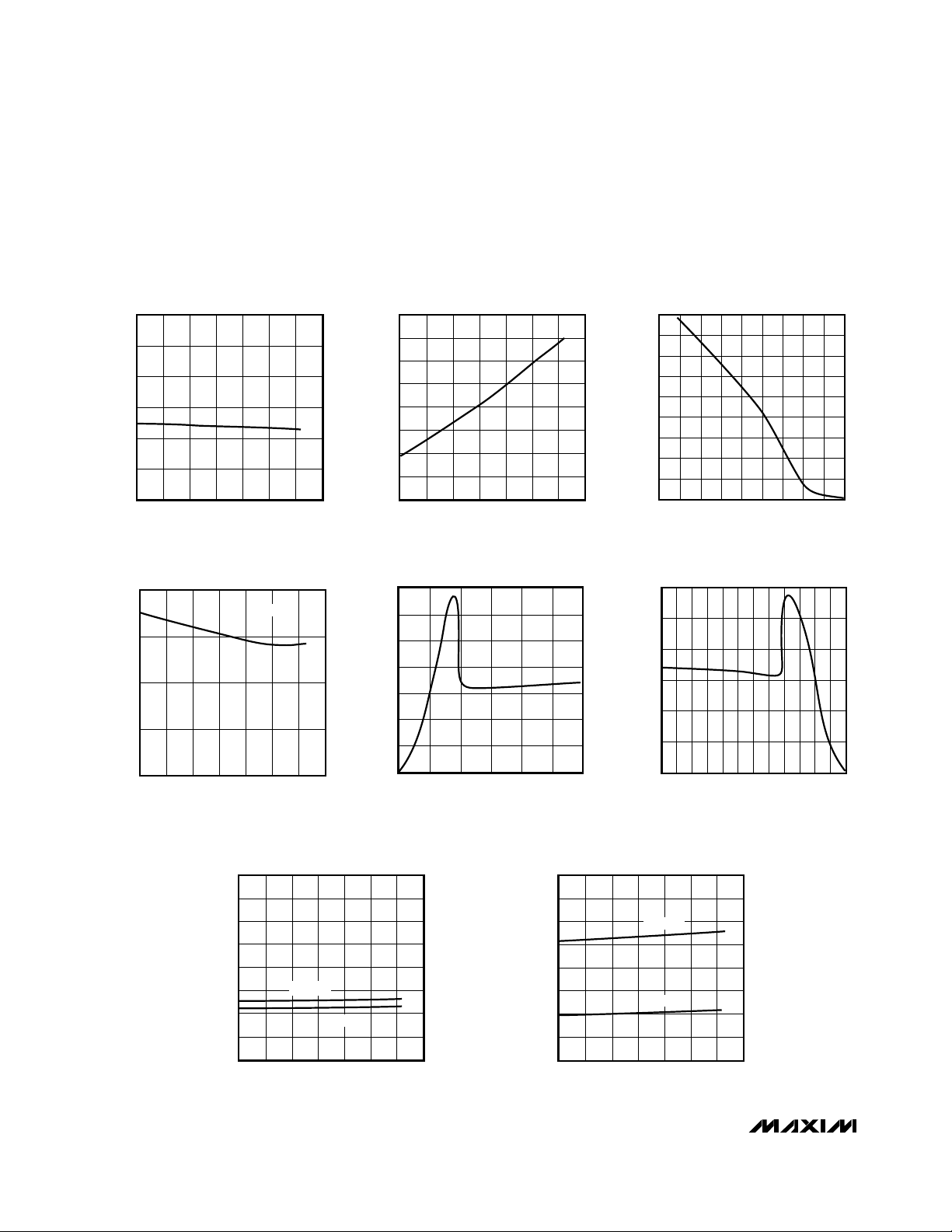
RECEIVER PROPAGATION DELAY
vs. TEMPERATURE
MAX1482-01
800
-40 -20 0 20 40 60 80 100
900
1000
1100
1200
1300
1400
TEMPERATURE (°C)
RECEIVER PROPAGATION DELAY (ns)
1200
400
500
-40 -20 20 80 100
DRIVER PROPAGATION DELAY
vs. TEMPERATURE
600
700
1000
1100
MAX1482-02
TEMPERATURE (°C)
DRIVER PROPAGATION DELAY (ns)
040
800
900
60
0
10
20
30
40
50
60
70
80
90
0.5 1.0 1.5 2.0 2.5 3.0 3.5 4.0 4.5 5.0
DRIVER OUTPUT CURRENT vs.
DIFFERENTIAL OUTPUT VOLTAGE
MAX1482-03
OUTPUT VOLTAGE (V)
OUTPUT CURRENT (mA)
DRIVER DIFFERENTIAL OUTPUT VOLTAGE
vs. TEMPERATURE
MAX1482-04
1.5
2.0
2.5
3.0
3.5
-40 -20 0 20 40 60 80 100
TEMPERATURE (°C)
DIFFERENTIAL OUTPUT VOLTAGE (V)
R = 54Ω
80
0
10
-40 -20 20 80 100
MAX1482
SUPPLY CURRENT
vs. TEMPERATURE
20
30
60
70
MAX1482-07
TEMPERATURE (°C)
SUPPLY CURRENT (µA)
040
40
50
60
DE = V
CC
DE = 0V
0
20
40
60
80
100
120
140
0246 10812
OUTPUT CURRENT vs.
DRIVER OUTPUT LOW VOLTAGE
MAX1482-05
OUTPUT LOW VOLTAGE (V)
OUTPUT CURRENT (mA)
0
20
40
60
80
100
120
-7 -6 -4 -2 0 2 4-5 -3 -1 315
OUTPUT CURRENT vs.
DRIVER OUTPUT HIGH VOLTAGE
MAX1482-06
OUTPUT LOW VOLTAGE (V)
OUTPUT CURRENT (mA)
80
0
10
-40 -20 20 80 100
MAX1483
SUPPLY CURRENT
vs. TEMPERATURE
20
30
60
70
MAX1482-08
TEMPERATURE (°C)
SUPPLY CURRENT (µA)
040
40
50
60
DE = V
CC
DE = GND
__________________________________________Typical Operating Characteristics
(TA = +25°C, unless otherwise noted.)
Page 5
MAX1482/MAX1483
20µA, 1⁄8-Unit-Load, Slew-Rate-Limited
RS-485 Transceivers
_______________________________________________________________________________________ 5
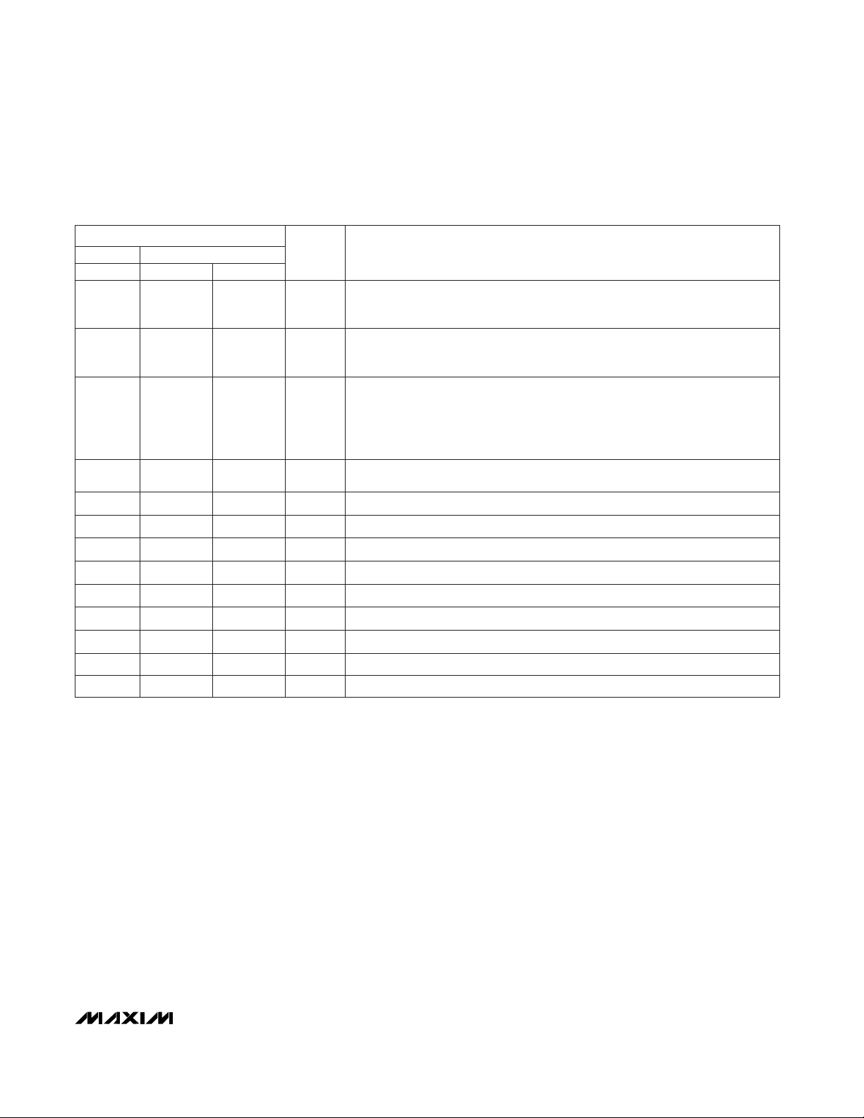
PIN
1, 8, 13
MAX1482
DIP/SO
FUNCTION
2 1
Receiver Output. With the receiver output enabled (RE low), RO is high if
A > B by 200mV or when A and B are not connected, and RO is low if A < B
by 200mV.
DIP/SO
3 2
Receiver Output Enable. When RE is low, RO is enabled. When RE is high, RO
is high impedance. If RE is high and DE is low, the MAX1482/MAX1483 enter
a low-power (0.1µA) shutdown state.
4 3
Driver Output Enable. The driver outputs, A and B, (Y and Z for the MAX1482)
are enabled by bringing DE high. When DE is low, the driver outputs are high
impedance, and the devices can function as line receivers if RE is low. If RE is
high and DE is low, the parts will enter a low-power (0.1µA) shutdown state. If
the driver outputs are enabled, the devices function as line drivers.
10 — Inverting Driver Output
9 — Noninverting Driver Output
6, 7 5 Ground
5 4
Driver Input. With DE high, a low on DI forces output Y low and output Z high,
and a high on DI forces output Y high and output Z low.
14 8 Positive Supply: 4.75V to 5.25V
11 — Inverting Receiver Input
— 7 Inverting Receiver Input and Inverting Driver Output
12 — Noninverting Receiver Input
— 6 Noninverting Receiver Input and Noninverting Driver Output
—
MAX1483
3
4
5
—
—
7
6
2
—
1
—
8
—
NAME
RO
RE
DE
Z
Y
GND
DI
V
CC
B
B
A
A
N.C. No Connect—not internally connected
µMAX
______________________________________________________________Pin Description
Page 6

MAX1482/MAX1483
20µA, 1⁄8-Unit-Load, Slew-Rate-Limited
RS-485 Transceivers
6 _______________________________________________________________________________________
Figure 1. Driver DC Test Load
Figure 3. Driver/Receiver Timing Test Circuit Figure 4. Driver Timing Test Load
Figure 2. Receiver Timing Test Load
R
R
Y
Z
V
OD
V
OC
_________________________________________________________________Test Circuits
3V
DE
DI
Y
V
ID
Z
C
L1
R
DIFF
C
L2
A
B
RECEIVER
OUTPUT
TEST POINT
C
RL
15pF
S1
1k
S2
1k
V
CC
V
RO
RE
OUTPUT
UNDER TEST
500Ω
C
L
S1
S2
CC
Page 7

MAX1482/MAX1483
20µA, 1⁄8-Unit-Load, Slew-Rate-Limited
RS-485 Transceivers
_______________________________________________________________________________________ 7
Figure 5. Driver Propagation Delays
Figure 8. Receiver Enable and Disable TimesFigure 7. Receiver Propagation Delays
Figure 6. Driver Enable and Disable Times
DI
3V
0V
Z
Y
V
O
0V
-V
O
V
O
1.5V
t
PLH
1/2 V
O
10%
t
R
90%
90%
t
PHL
1.5V
1/2 V
O
10%
t
F
V
DIFF
= V (Y) - V (Z)
V
DIFF
t
SKEW =
| t
PLH
- t
PHL
|
_______________________________________________________Switching Waveforms
3V
V
OH
RO
A-B
V
OL
V
ID
0V
-V
ID
1.5V
t
PHL
INPUT
OUTPUT
t
PLH
1.5V
DE
0V
Y, Z
V
Y, Z
0V
3V
RE
0V
V
CC
RO
0V
RO
0V
1.5V 1.5V
, t
t
ZL(SHDN)
ZL
2.3V
OL
1.5V 1.5V
OUTPUT NORMALLY LOW
OUTPUT NORMALLY HIGH
2.3V
t
, t
ZH(SHDN)
ZH
, t
t
ZL(SHDN)
ZL
1.5V
OUTPUT NORMALLY LOW
OUTPUT NORMALLY HIGH
1.5V
t
, t
ZH(SHDN)
ZH
t
LZ
V
+ 0.5V
OL
V
- 0.5V
OH
t
HZ
t
LZ
VOL + 0.5V
V
- 0.5V
OH
t
HZ
Page 8

MAX1482/MAX1483
__________Applications Information
The MAX1482/MAX1483 are low-power transceivers for
RS-485 and RS-422 communications. The MAX1482
and MAX1483 are specified for data rates of at least
250kbps. The MAX1482 is a full-duplex transceiver
while the MAX1483 is half duplex. When disabled, the
driver and receiver outputs are high impedance.
The 96kΩ, 1/8-unit-load receiver input impedance of the
MAX1482/MAX1483 allows up to 256 transceivers on a
bus, compared to the 1-unit load (12kΩ input impedance) of standard RS-485 drivers (32 transceivers maximum). Any combination of MAX1482/MAX1483 and
other RS-485 transceivers with a total of 32 unit loads or
less can be put on the bus.
Reduced EMI and Reflections
The MAX1482/MAX1483 are slew-rate limited, minimizing EMI and reducing reflections caused by improperly
terminated cables. Figure 9 shows both the driver output waveform of a MAX1482/MAX1483 transmitting a
125kHz signal and the Fourier analysis of that signal.
High-frequency harmonics have much lower amplitudes, and the potential for EMI is significantly reduced.
20µA, 1⁄8-Unit-Load, Slew-Rate-Limited
RS-485 Transceivers
8 _______________________________________________________________________________________
Figure 9. Driver Output Waveform and FFT, Transmitting
250kbps (125kHz) Signal
Figure 10. Receiver Propagation-Delay Test Circuit
Table 1. Transmitting Table 2. Receiving
INPUTS OUTPUTS
RE
DE DI Z Y
X
X
X
1
1
0
1
0
X
0
1
High-Z
1
0
High-Z
X = Don't Care
High-Z = High Impedance
10dB/div
0Hz 500kHz/div 5MHz
100pF
Z
D
Y
R = 54Ω
100pF
, tF < 6ns
t
R
TTL IN
B
A
RECEIVER
R
OUT
RE DE
0
0
0
1
X = Don't Care
High-Z = High Impedance
DE = 0 for MAX1483 and is a Don't Care for MAX1482.
*
INPUTS OUTPUT
*
0
0
0
0
A-B RO
> +0.2V
< -0.2V
Inputs open
X
1
0
1
High-Z
Page 9

Low-Power Shutdown Mode
A low-power shutdown mode is initiated by bringing RE
high and DE low. The devices will not shut down unless
both the driver and receiver are disabled. In shutdown, the devices typically draw only 0.1µA of supply
current.
RE and DE may be driven simultaneously; the parts are
guaranteed not to enter shutdown if RE is high and DE
is low for less than 50ns. If the inputs are in this state for
at least 600ns, the parts are guaranteed to enter shutdown.
For the receiver, the t
ZH
and tZLenable times assume
the part was not in the low-power shutdown state. The
t
ZH(SHDN)
and t
ZL(SHDN)
enable times assume the
parts were shut down (see Electrical Characteristics).
It takes the receivers longer to become enabled from
the low-power shutdown state (t
ZH(SHDN)
, t
ZL(SHDN)
)
than from the operating mode (t
ZH
, tZL). (The parts are
in operating mode if the RE , DE inputs equal a logical
0,1 or 1,1 or 0,0.)
Driver Output Protection
Excessive output current and power dissipation caused
by faults or by bus contention are prevented by two
mechanisms. A foldback current limit on the output
stage provides immediate protection against short circuits over the whole common-mode voltage range (see
Typical Operating Characteristics). In addition, a thermal shutdown circuit forces the driver outputs into a
high-impedance state if the die temperature rises
excessively.
Propagation Delay
Digital encoding schemes depend on the driver and
receiver skew. Skew is defined as the difference
between the rising and falling propagation delay times.
Typical propagation delays are shown in Figures 11
and 12 using Figure 10’s test circuit.
The difference in receiver delay times, | t
PLH
- t
PHL
|, is
typically under 160ns.
The driver skew times are typically 160ns (800ns max).
MAX1482/MAX1483
20µA, 1⁄8-Unit-Load, Slew-Rate-Limited
RS-485 Transceivers
_______________________________________________________________________________________ 9
RO
5V/div
B
A
500mV/div
500ns/div
Figure 11. Receiver t
PHL
Figure 12. Receiver t
PLH
B
500mV/div
A
5V/div
RO
500ns/div
Page 10

MAX1482/MAX1483
Line Length vs. Data Rate
The RS-485/RS-422 standard covers line lengths up to
4000 feet. For line lengths greater than 4000 feet, see
Figure 16.
Figure 13 shows the system differential voltage for the
parts driving 4000 feet of 26AWG twisted-pair wire at
110kHz into 120Ω loads. Even after 4000 feet of cable,
the MAX1482/MAX1483 output shows virtually no distortion.
Typical Applications
The MAX1482/MAX1483 transceivers are designed for
bidirectional data communications on multipoint bus
transmission lines. Figures 14 and 15 show typical network applications circuits. These parts can also be
used as line repeaters, with cable lengths longer than
4000 feet, as shown in Figure 16.
To minimize reflections, the line should be terminated at
both ends in its characteristic impedance, and stub
lengths off the main line should be kept as short as
possible (although the slew-rate-limited MAX1482 and
MAX1483 are more tolerant of imperfect termination
than standard RS-485 ICs).
Isolated RS-485
For isolated RS-485 applications, see the MAX253 and
MAX1480 data sheets.
20µA, 1⁄8-Unit-Load, Slew-Rate-Limited
RS-485 Transceivers
10 ______________________________________________________________________________________
DI RO DE
RE
A
B
RE
RERE
RO
RO
RO
DI
DI
DI
DE
DE
DE
D
D
D
R
R
R
B
B
B
A
A
A
120Ω
120Ω
D
R
MAX1483
Figure 14. MAX1483 Typical Half-Duplex RS-485 Network
R
O
DI
RECEIVER
INPUT
V
Y-VZ
2µs/div
5
0
1
0
-1
5
0
Figure 13. System Differential Voltage at 250kbps (125kHz)
Driving 4000 Feet of Cable
Page 11

MAX1482/MAX1483
20µA, 1⁄8-Unit-Load, Slew-Rate-Limited
RS-485 Transceivers
______________________________________________________________________________________ 11
120Ω
120Ω
R
D
RO
RE
DE
DI
A
B
Y
120Ω
120Ω
DI
DI DIRO RO
RO
DE DE
DE
RE
RE
RE
Z
Z
Z
Z
Y
Y
Y
AA
A
BB
B
D
D
D
R
R
R
NOTE: RE AND DE ON.
MAX1482
Figure 15. MAX1482 Full-Duplex RS-485 Network
Figure 16. Line Repeater for MAX1482
120Ω
120Ω
DATA IN
DATA OUT
R
D
RO
RE
DE
DI
A
B
Z
Y
NOTE: RE AND DE ON.
MAX1482
Typical Operating Circuits
________________________(continued)
DE V
CC
144
MAX1482
9
5
DI
RO
N.C.
D
2
1, 8, 13
3 6, 7
RE GND
Y
10
Z
12
A
RD
Rt
11
B
VCCRE
Rt
R
GND DE
RO
DI
Page 12

MAX1482/MAX1483
20µA, 1⁄8-Unit-Load, Slew-Rate-Limited
RS-485 Transceivers
12 ______________________________________________________________________________________
__________________Chip Information____Pin Configurations (continued)
DIP/SO
TOP VIEW
1
2
3
4
5
6
7
14
13
12
11
10
9
8
V
CC
N.C.
N.C.
A
B
Z
Y
N.C.
RO
RE
DE
DI
GND
GND
R
D
MAX1482
TRANSISTOR COUNT: 294
L
α
C
A1B
DIM
A
A1
B
C
D
E
e
H
L
α
MIN
0.036
0.004
0.010
0.005
0.116
0.116
0.188
0.016
0°
MAX
0.044
0.008
0.014
0.007
0.120
0.120
0.198
0.026
6°
MIN
0.91
0.10
0.25
0.13
2.95
2.95
4.78
0.41
0°
MAX
1.11
0.20
0.36
0.18
3.05
3.05
5.03
0.66
6°
INCHES MILLIMETERS
8-PIN µMAX
MICROMAX SMALL OUTLINE
PACKAGE
0.650.0256
A
e
E H
D
0.101mm
0.004 in
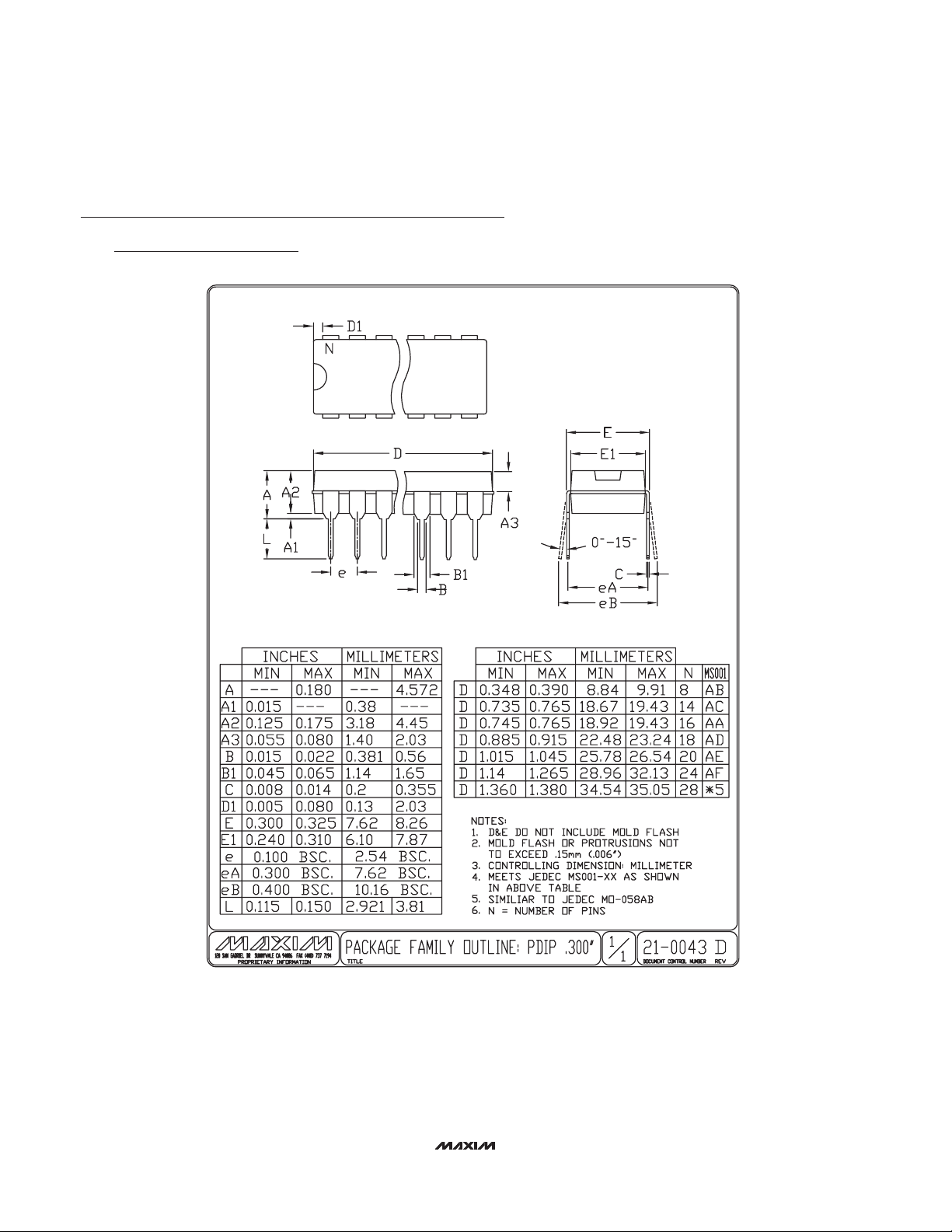
Package Information
(The package drawing(s) in this data sheet may not reflect the most current specifications. For the latest package outline information,
go to www.maxim-ic.com/packages
.)
Page 13

MAX1482/MAX1483
20µA, 1⁄8-Unit-Load, Slew-Rate-Limited
RS-485 Transceivers
______________________________________________________________________________________ 13
SOICN .EPS
PACKAGE OUTLINE, .150" SOIC
1
1
21-0041
B
REV.DOCUMENT CONTROL NO.APPROVAL
PROPRIETARY INFORMATION
TITLE:
TOP VIEW
FRONT VIEW
MAX
0.010
0.069
0.019
0.157
0.010
INCHES
0.150
0.007
E
C
DIM
0.014
0.004
B
A1
MIN
0.053A
0.19
3.80 4.00
0.25
MILLIMETERS
0.10
0.35
1.35
MIN
0.49
0.25
MAX
1.75
0.050
0.016L
0.40 1.27
0.3940.386D
D
MINDIM
D
INCHES
MAX
9.80 10.00
MILLIMETERS
MIN
MAX
16
AC
0.337 0.344 AB8.758.55 14
0.189 0.197 AA5.004.80 8
N MS012
N
SIDE VIEW
H 0.2440.228 5.80 6.20
e 0.050 BSC 1.27 BSC
C
HE
e
B
A1
A
D
0∞-8∞
L
1
VARIATIONS:
Package Information (continued)
(The package drawing(s) in this data sheet may not reflect the most current specifications. For the latest package outline information,
go to www.maxim-ic.com/packages
.)
Page 14
MAX1482/MAX1483
20µA, 1⁄8-Unit-Load, Slew-Rate-Limited
RS-485 Transceivers
Maxim cannot assume responsibility for use of any circuitry other than circuitry entirely embodied in a Maxim product. No circuit patent licenses are
implied. Maxim reserves the right to change the circuitry and specifications without notice at any time.
14 __________________Maxim Integrated Products, 120 San Gabriel Drive, Sunnyvale, CA 94086 (408) 737-7600
© 2006 Maxim Integrated Products is a registered trademark of Maxim Integrated Products, Inc.
PDIPN.EPS
Package Information (continued)
(The package drawing(s) in this data sheet may not reflect the most current specifications. For the latest package outline information,
go to www.maxim-ic.com/packages
.)
 Loading...