

Page 1
_________________General Description
The MAX1480EA/MAX1480EC/MAX1490EA/MAX1490EB
are complete, electrically isolated, RS-485/RS-422 data
communications interface solutions in a hybrid microcircuit. The RS-485/RS-422 I/O pins are protected against
±15kV electrostatic discharge (ESD) shocks, without
latchup. Transceivers, optocouplers, and a transformer
provide a complete interface in a standard DIP package.
A single +5V supply on the logic side powers both sides
of the interface.
The MAX1480EC/MAX1490EB feature reduced-slew-rate
drivers that minimize EMI and reduce reflections caused
by improperly terminated cables, allowing error-free data
transmission at data rates up to 160kbps. The
MAX1480EA/MAX1490EA driver slew rate is not limited,
allowing transmission rates up to 2.5Mbps. The
MAX1480EA/MAX1480EC are designed for half-duplex
communication, while the MAX1490EA/MAX1490EB feature full-duplex communication.
Drivers are short-circuit current limited and protected
against excessive power dissipation by thermal shutdown circuitry that places the driver outputs into a highimpedance state. The receiver input has a fail-safe
feature that guarantees a known output (RO low for the
MAX1480EA/MAX1480EC, RO high for the MAX1490EA/
MAX1490EB) if the input is open circuit.
The MAX1480EA/MAX1480EC/MAX1490EA/MAX1490EB
withstand 1260V
RMS
(1min) or 1520V
RMS
(1s). Their isolated outputs meet all RS-485/RS-422 specifications. The
MAX1480EA/MAX1480EC are available in a 28-pin DIP
package, and the MAX1490EA/MAX1490EB are available
in a 24-pin DIP package.
.
________________________Applications
Isolated RS-485/RS-422 Data Interface
Transceivers for EMI-Sensitive Applications
Industrial-Control Local Area Networks
Automatic Test Equipment
HVAC/Building Control Networks
Telecom
____________________________Features
♦ Isolated Data Interface, Guaranteed to 1260V
RMS
(1min)
♦ ±15kV ESD Protection on I/O Pins
♦ Slew-Rate Limited for Errorless Data
Transmission (MAX1480EC/MAX1490EB)
♦ High-Speed, Isolated, 2.5Mbps RS-485/RS-422
Interface (MAX1480EA/MAX1490EA)
♦ Full-Duplex Data Communication
(MAX1490EA/MAX1490EB)
♦ Single +5V Supply
♦ Current Limiting and Thermal Shutdown for
Driver Overload Protection
♦ Standard 0.6in DIP Packages
28-Pin DIP (MAX1480EA/MAX1480EC)
24-Pin DIP (MAX1490EA/MAX1490EB)
MAX1480E/MAX1490E
±15kV ESD-Protected, Isolated RS-485/RS-422
Data Interfaces
________________________________________________________________ Maxim Integrated Products 1
Pin Configurations
1
24
23
22
21
20
19
18
17
2
3
4
5
6
7
8
AC1
AC2
ISO V
CC1
ISO RO DRVD2
D1
A
B
Z
Y
SD
FS
GND1
16
15
14
13
9
10
11
12
ISO COM1
ISO DI DRV
ISO V
CC2
ISO RO LED
GND2
RO
DI
DIP
V
CC2
V
CC3
V
CC4
V
CC1
MAX1490EA/
MAX1490EB
MAX845E
MAX488E
MAX490E
TOP VIEW
ISOLATION BARRIER
19-1940; Rev 0; 4/01
PART
†
MAX1480EACPI
MAX1480EAEPI -40°C to +85°C
0°C to +70°C
TEMP. RANGE PIN-PACKAGE
28 Wide Plastic DIP*
28 Wide Plastic DIP*
_______________Ordering Information
Ordering Information continued at end of data sheet.
†
Data rate for A parts is up to 2.5Mbps. Data rate for C parts is
up to 250kbps.
*See Reliability section at end of data sheet.
Pin Configurations continued at end of data sheet.
Selector Guide appears at end of data sheet.
For pricing, delivery, and ordering information, please contact Maxim/Dallas Direct! at
1-888-629-4642, or visit Maxim’s website at www.maxim-ic.com.
Page 2
mA
MAX1480E/MAX1490E
±15kV ESD-Protected, Isolated RS-485/RS-422
Data Interfaces
2 _______________________________________________________________________________________
ABSOLUTE MAXIMUM RATINGS
ELECTRICAL CHARACTERISTICS
(V
CC_
= +5V ±10%, VFS= V
CC_
, TA= T
MIN
to T
MAX
, unless otherwise noted. Typical values are at V
CC_
= +5V and TA= +25°C.)
(Notes 1, 2)
Stresses beyond those listed under “Absolute Maximum Ratings” may cause permanent damage to the device. These are stress ratings only, and functional
operation of the device at these or any other conditions beyond those indicated in the operational sections of the specifications is not implied. Exposure to
absolute maximum rating conditions for extended periods may affect device reliability.
With Respect to GND_
Supply Voltage (V
CC_
)..........................................-0.3V to +6V
Control Input Voltage (SD, FS)..............-0.3V to (V
CC_
+ 0.3V)
Receiver Output Voltage (RO, RO).......-0.3V to (V
CC_
+ 0.3V)
Output Switch Voltage (D1, D2).......................................+12V
With Respect to ISO COM_
Control Input Voltage (ISO DE_) ....-0.3V to (ISO V
CC_
+ 0.3V)
Driver Input Voltage (ISO DI_) .......-0.3V to (ISO V
CC_
+ 0.3V)
Receiver Output Voltage (ISO RO_)
..-0.3V to (ISO V
CC_
+ 0.3V)
Driver Output Voltage (A, B, Y, Z) ......................-8V to +12.5V
Receiver Input Voltage (A, B).............................-8V to +12.5V
LED Forward Current (DI, DE, ISO RO LED) ......................50mA
Continuous Power Dissipation (T
A
= +70°C)
24-Pin Plastic DIP (derate 8.7mW°C above +70°C) ....696mW
28-Pin Plastic DIP (derate 9.09mW/°C above +70°C) .727mW
Operating Temperature Ranges
MAX1480E_CPI/MAX1490E_CPI ........................0°C to +70°C
MAX1480E_EPI/MAX1490E_EPI......................-40°C to +85°C
Storage Temperature Range .............................-65°C to +150°C
Lead Temperature (soldering, 10s) .................................+300°C
Operating Supply Current I
CC
1.5 5R = 27Ω (RS-485), Figure 4
R = 50Ω (RS-422)
V
2
V
OD2
Differential Driver Output
(with Load)
VFS= 0
CONDITIONS
535f
SWL
UNITSMIN TYP MAXSYMBOLPARAMETER
FS = V
CC_
or open 725f
SWH
85 120
55 120
MAX1480EA,
DE
´ = V
CC_
or open
145
130
Low
V
0.8V
SDL
MAX1480EC,
DE
´ = V
CC_
or open
Shutdown Input Threshold
SD = V
CC_
High
µA0.2I
SHDN
Shutdown Supply Current
(Note 3)
2.4V
SDH
120
65 125
High
Low
2.4V
FSH
V
0.8V
FSL
FS Input Threshold
DE´, DI´, Figures 1 and 2
DE´, DI´, Figures 1 and 2
VVCC- 0.4V
IH
Input High Voltage
V0.4V
IL
Input Low Voltage
FS low
FS high
µA50FS Input Pullup Current
pA10FS Input Leakage Current
pA10
Shutdown Input Leakage
Current
RL= ∞
RL= 54Ω
RL= ∞
RL= 54Ω
RL= ∞
MAX1490EB
RL= 54Ω
TA= +25°C, f = 1MHz pF10C
ISO
Isolation Capacitance
TA= +25°C, V
ISO
= 50VDC MΩ100 10,000R
ISO
Isolation Resistance
kHzSwitch Frequency
mA
RL= ∞
RL= 54Ω
130 180
MAX1490EA
180
V8V
OD1
Differential Driver Output
(No Load)
TA= +25°C, 1min (Note 4) V
RMS
1260V
ISO
Isolation Voltage
Page 3
MAX1480E/MAX1490E
±15kV ESD-Protected, Isolated RS-485/RS-422
Data Interfaces
_______________________________________________________________________________________ 3
ELECTRICAL CHARACTERISTICS (continued)
(V
CC_
= +5V ±10%, VFS= V
CC_
, TA= T
MIN
to T
MAX
, unless otherwise noted. Typical values are at V
CC_
= +5V and TA= +25°C.)
(Notes 1, 2)
SWITCHING CHARACTERISTICS—MAX1480EA/MAX1490EA
(V
CC_
= +5V ±10%, VFS= V
CC_
, TA= T
MIN
to T
MAX
, unless otherwise noted. Typical values are at V
CC_
= +5V and TA= +25°C.)
Driver Disable Time from Low
(MAX1480EA Only)
t
LZ
0.5 1.8 µsFigures 6 and 8, CL= 15pF, S1 closed
Driver Disable Time from High
(MAX1480EA Only)
t
HZ
0.5 1.8 µsFigures 6 and 8, CL= 15pF, S2 closed
Driver Enable to Output Low
(MAX1480EA Only)
t
ZL
1.0 1.8 µsFigures 6 and 8, CL= 100pF, S1 closed
PARAMETER SYMBOL MIN TYP MAX UNITS
Driver Rise or Fall Time t
R, tF
15 50 ns
Receiver Input to Output
Propagation Delay
t
PHL
90 225
ns
Figures 5 and 7, R
DIFF
= 54Ω, CL1= CL2= 100pF
t
PLH
120 225
Driver Enable to Output High
(MAX1480EA Only)
t
ZH
1.0 1.8 µs
Figures 5 and 10, R
DIFF
= 54Ω, CL1= CL2= 100pF
Figures 6 and 8, CL= 100pF, S2 closed
t
PLH
90 275
Figures 5 and 7, R
DIFF
= 54Ω,
CL1= CL2= 100pF
Driver Output Skew
CONDITIONS
t
SKEW
30 100 ns
Driver Input to Output
Propagation Delay
t
PHL
60 275
ns
Figures 5 and 7, R
DIFF
= 54Ω, CL1= CL2= 100pF
-7V ≤ VCM≤ +12V VV
TH
Receiver Differential Threshold
A, B, Y, and Z pins, tested using Human Body
Model, Figures 1 and 2
kVISO I
OSD
ESD Protection
R = 27Ω or 50Ω, Figure 4 V
0.3
∆V
OD
CONDITIONS
Change in Magnitude of
Driver Output Voltage for
Complementary Output States
mA
0.25
R = 27Ω or 50Ω, Figure 4
VCM= 0
kΩR
IN
Receiver Input Resistance
mV∆V
TH
Receiver Input Hysteresis
V4V
OC
Driver Common-Mode Output
1.0
UNITSMIN TYP MAXSYMBOLPARAMETER
V
OUT
= 5.5V µAI
OH
Receiver Output High Current
Using resistor values listed in Tables 1 and 2
-7V ≤ VO≤ 12V (Note 5) mAISO I
OSD
Driver Short-Circuit Current
VV
OL
Receiver Output Low Voltage
Differential
Common mode 0.3
MAX1490EA/
MAX1490EB
MAX1480EA/
MAX1480EC
MAX1480EA/
MAX1480EC
MAX1490EA/
MAX1490EB
0.2
ISO I
IN
Input Current (A, B)
0.8
DE´ = 0,
V
CC_
= 0 or +5.5V
VIN= +12V
VIN= -7V
12
-0.2 0.2
70
0.4
250
100
±15
-7V ≤ VCM≤ +12V
48
(MAX1490E_)
(MAX1480E_)
Page 4
MAX1480E/MAX1490E
±15kV ESD-Protected, Isolated RS-485/RS-422
Data Interfaces
4 _______________________________________________________________________________________
Note 1: All currents into device pins are positive; all currents out of device pins are negative. All voltages are referenced to logic-
side ground (GND_), unless otherwise specified.
Note 2: For DE
´ and DI´ pin descriptions, see Detailed Block Diagram and Typical Application Circuit (Figure 1 for MAX1480EA/
MAX1480EC, Figure 2 for MAX1490EA/MAX1490EB).
Note 3: Shutdown supply current is the current at V
CC1
and V
CC2
when shutdown is enabled.
Note 4: Limit guaranteed by applying 1520V
RMS
for 1s. Test voltage is applied between all pins on one side of the package to all
pins on the other side of the package, e.g., between pins 1–14 and pins 15–28 on the 28-pin package.
Note 5: Applies to peak current (see Typical Operating Characteristics). Although the MAX1480EA/MAX1480EC and
MAX1490EA/MAX1490EB provide electrical isolation between logic ground and signal paths, they do not provide isolation
between external shields and the signal paths (see Isolated Common Connection section).
SWITCHING CHARACTERISTICS—MAX1480EA/MAX1490EA (continued)
(V
CC_
= +5V ±10%, VFS= V
CC_
, TA= T
MIN
to T
MAX
, unless otherwise noted. Typical values are at V
CC_
= +5V and TA= +25°C.)
t
ZH(SHDN)
315Figures 6 and 9, CL= 100pF, S2 closedShutdown to Driver Output High
t
ZH(SHDN)
315
µs
Figures 6 and 9, CL= 100pF, S1 closed
PARAMETER SYMBOL MIN TYP MAX UNITSCONDITIONS
Shutdown to Driver Output Low µs
t
PLH
1.4 3.0Figures 5 and 7, R
DIFF
= 54Ω, CL1= CL2= 100pF
Driver Input to Output
Propagation Delay
t
PHL
1.1 3.0
µs
Figures 5 and 7, R
DIFF
= 54Ω, CL1= CL2= 100pF
Driver Disable Time from High
(MAX1480EC Only)
t
HZ
1.7 4.5 µsFigures 6 and 8, CL= 15pF, S2 closed
Driver Disable Time from Low
(MAX1480EC Only)
t
LZ
2.0 4.5 µsFigures 6 and 8, CL= 15pF, S1 closed
Driver Enable to Output Low
(MAX1480EC Only)
t
ZL
1.4 4.5 µsFigures 6 and 8, CL= 100pF, S1 closed
Driver Enable to Output High
(MAX1480EC Only)
t
ZH
1.4 4.5 µsFigures 6 and 8, CL= 100pF, S2 closed
Time to Shutdown t
SHDN
100 µs
PARAMETER SYMBOL MIN TYP MAX UNITS
Driver Rise or Fall Time t
R, tF
1.0 2.0 µs
|t
PLH
- t
PHL
| Differential
Receiver Skew
t
SKD
200 ns
Receiver Input to Output
Propagation Delay
t
PHL
1.1 3.0
µs
Figures 5 and 10, R
DIFF
= 54Ω, CL1= CL2= 100pF
Maximum Data Rate
Figures 5 and 7, R
DIFF
= 54Ω, CL1= CL2= 100pF
f
MAX
160 kbps
Shutdown to Driver Output Low
t
SKEW
, t
SKD
≤ 25% of data period
t
ZL(SHDN)
t
PLH
0.9 3.0
315
Figures 5 and 10, R
DIFF
= 54Ω, CL1= CL2= 100pF
µsFigures 6 and 9, CL= 100pF, S1 closed
Shutdown to Driver Output High t
ZH(SHDN)
315µsFigures 6 and 9, CL= 100pF, S2 closed
Driver Output Skew
CONDITIONS
t
SKEW
300 1200 nsFigures 5 and 7, R
DIFF
= 54Ω, CL1= CL2= 100pF
t
SKD
30 150Figures 5 and 10, R
DIFF
= 54Ω, CL1= CL2= 100pF
|t
PLH
- t
PHL
| Differential
Receiver Skew
ns
SWITCHING CHARACTERISTICS—MAX1480EC/MAX1490EB
(V
CC_
= +5V ±10%, VFS= V
CC_
, TA= T
MIN
to T
MAX
, unless otherwise noted. Typical values are at V
CC_
= +5V and TA= +25°C.)
t
SHDN
100Time to Shutdown µs
f
MAX
2.5t
SKEW
, t
SKD
, t
PHL
≤ 25% of data periodMaximum Data Rate Mbps
Page 5
MAX1480E/MAX1490E
±15kV ESD-Protected, Isolated RS-485/RS-422
Data Interfaces
_______________________________________________________________________________________ 5
__________________________________________Typical Operating Characteristics
(V
CC_
= +5V, VFS= V
CC_
, Figures 1 and 2, TA = +25°C, unless otherwise noted.)
OUTPUT CURRENT vs.
RECEIVER OUTPUT LOW VOLTAGE
80
MEASURED AT ISO RO DRV
70
60
50
40
30
OUTPUT CURRENT (mA)
20
10
0
1.00.50 3.53.02.52.0 5.04.54.0
OUTPUT LOW VOLTAGE (V)
RECEIVER OUTPUT LOW VOLTAGE
vs. TEMPERATURE
0.8
MEASURED AT ISO RO DRV
I
= 8mA
RO
0.7
0.6
0.5
0.4
0.3
OUTPUT LOW VOLTAGE (V)
0.2
0.1
0
-40 20
DRIVER OUTPUT CURRENT
vs. DIFFERENTIAL OUTPUT VOLTAGE
80
70
60
50
40
30
OUTPUT CURRENT (mA)
20
10
0
1.00.50 3.53.02.52.0 5.04.54.0
DIFFERENTIAL OUTPUT VOLTAGE (V)
OUTPUT CURRENT vs.
RECEIVER OUTPUT HIGH VOLTAGE
-30
MEASURED AT ISO RO DRV
-25
MAX1480E/90E TOC01
-20
-15
-10
OUTPUT CURRENT (mA)
-5
1.5
0
1.00.50 3.53.02.52.0 5.04.54.0
1.5
OUTPUT HIGH VOLTAGE (V)
OUTPUT CURRENT vs.
DRIVER OUTPUT LOW VOLTAGE
180
160
140
MAX1480E/90E TOC04
120
100
80
60
OUTPUT CURRENT (mA)
40
20
0
123456789101112
0-20 6040 80
TEMPERATURE (°C)
0
OUTPUT LOW VOLTAGE (V)
DRIVER DIFFERENTIAL OUTPUT VOLTAGE
vs. TEMPERATURE
3.0
DI´ = HIGH OR OPEN
MAX1480E/90E TOC07
1.5
DI´ = HIGH OR OPEN
2.9
= 54Ω
R
L
2.8
2.7
2.6
2.5
2.4
2.3
2.2
DIFFERENTIAL OUTPUT VOLTAGE (V)
2.1
2.0
-40 20
0-20 6040 80
TEMPERATURE (°C)
5.00
MEASURED AT ISO RO DRV
I
4.75
4.50
MAX1480E/90E TOC02
4.25
4.00
3.75
OUTPUT HIGH VOLTAGE (V)
3.50
3.25
3.00
-40 20
-100
-90
-80
MAX1480E/90E TOC05
-70
-60
-50
-40
-30
OUTPUT CURRENT (mA)
-20
-10
0
-7
0.40
0.35
0.30
MAX1480E/90E TOC08
0.25
0.20
0.15
SHUTDOWN CURRENT (µA)
0.10
0.05
0
-40 20
RECEIVER OUTPUT HIGH VOLTAGE
vs. TEMPERATURE
= 8mA
RO
0-20 6040 80
TEMPERATURE (°C)
OUTPUT CURRENT vs.
DRIVER OUTPUT HIGH VOLTAGE
-6 -5 -4 -3 -2 -1 1 2 3 4 5 6
OUTPUT HIGH VOLTAGE (V)
0
SHUTDOWN CURRENT
vs. TEMPERATURE
SD = V
, DI´ = V
CC_
DE´= V
MEASURED AT V
CC_
(MAX1480EC ONLY)
CC_
AND V
CC1
CC2
0-20 6040 80
TEMPERATURE (°C)
MAX1480E/90E TOC03
MAX1480E/90E TOC06
MAX1480E/90E TOC09
Page 6
MAX1480E/MAX1490E
±15kV ESD-Protected, Isolated RS-485/RS-422
Data Interfaces
6 _______________________________________________________________________________________
____________________________Typical Operating Characteristics (continued)
(V
CC_
= +5V, VFS= V
CC_
, Figures 1 and 2, TA = +25°C, unless otherwise noted.)
V
CC_
= 5.0V, DE´= V
CC_
MAX1480EA/MAX1490EA
RECEIVER t
PHL
RO
2V/div
20ns/div
RECEIVER
INPUT A
1V/div
RECEIVER
INPUT B
1V/div
MAX1480E/90E toc14
V
CC_
= 5.0V, DE´= V
CC_
MAX1480EA/MAX1490EA
RECEIVER t
PLH
RO
2V/div
20ns/div
RECEIVER
INPUT B
1V/div
RECEIVER
INPUT A
1V/div
MAX1480E/90E toc15
SUPPLY CURRENT vs. TEMPERATURE
160
DE´ = V
V
CC
V
V
CC
= +5.5V
140
120
100
80
60
SUPPLY CURRENT (mA)
40
20
0
-40 -20 0 20 40 60 80
MAX1480EA
SUPPLY CURRENT vs. TEMPERATURE
= +5.5V
CC
= +5V
V
CC
= +4.5V
CC
V
= +4.5V
V
CC
TEMPERATURE (°C)
= 54Ω
R
L
= ∞
R
L
= +5V
CC
120
110
100
MAX1480E/90E TOC10
90
80
70
60
50
SUPPLY CURRENT (mA)
40
30
20
-40 -20 0 20 40 60 80
DE´ = V
V
CC
V
CC
V
CC
CC
= +5V
V
CC
TEMPERATURE (°C)
MAX1480EC
= +5.5V
= +5V
= +4.5V
= +5.5V
V
CC
SUPPLY CURRENT vs. TEMPERATURE
MAX1490EA
= 54Ω
R
L
= ∞
R
L
= +4.5V
V
CC
200
180
MAX1480E/90E T0C11
160
140
120
SUPPLY CURRENT (mA)
100
= +5.5V
V
CC
= +5V
V
CC
= +4.5V
V
CC
= +5.5V
V
CC
= +5V
V
CC
= +4.5V
V
80
-40 -20 0 20 40 60 80
TEMPERATURE (°C)
CC
R
L
R
L
= 54Ω
= ∞
MAX1480E/90E TOC12
SUPPLY CURRENT vs. TEMPERATURE
150
140
130
120
110
100
90
80
SUPPLY CURRENT (mA)
70
60
50
-40 -20 0 20 40 60 80
MAX1490EB
V
V
= +5V
V
CC
TEMPERATURE (°C)
V
CC
CC
CC
= +5.5V
= +5V
= +4.5V
V
CC
= +5.5V
MAX1480E/90E TOC13
= 54Ω
R
L
= ∞
R
L
= +4.5V
V
CC
Page 7

MAX1480E/MAX1490E
±15kV ESD-Protected, Isolated RS-485/RS-422
Data Interfaces
_______________________________________________________________________________________ 7
_____________________________Typical Operating Characteristics (continued)
(V
CC_
= +5V, VFS= V
CC_
, V
DI
´
= 0, DE
´ toggled 0 to 5V at 5kHz, Figures 1 and 2, T
A
= +25°C, unless otherwise noted.)
V
= 5.0V, DI´ = 0V
MAX1480EC
DRIVER DISABLE TIME
DE´
2V/div
500ns/div
DRIVER
OUTPUT B
2V/div
MAX1480E/90E TOC19
MAX1480EC/MAX1490EB
200ns/div
PHL
RECEIVER t
´
MAX1480EC
DRIVER ENABLE TIME
MAX1480E/90E toc16
RECEIVER
INPUT A
1V/div
RECEIVER
INPUT B
1V/div
RO
2V/div
MAX1480E/90E TOC18
DRIVER
OUTPUT B
2V/div
MAX1480EC/MAX1490EB
RECEIVER t
PLH
500ns/div
´
MAX1480E/90E toc17
RECEIVER
INPUT A
1V/div
RECEIVER
INPUT B
1V/div
RO
2V/div
V
= 5.0V, DI´= 0V
DE´
2V/div
500ns/div
MAX1480EA/MAX1490EA
POWER-UP DELAY TO DRIVER OUTPUTS VALID
DRIVER
MAX1480E/90E TOC20
OUTPUT B
(Z FOR MAX1490)
2V/div
SD
2V/div
V
= 0
DI´
= 5V TO 0 AT 1kHz
V
SD
1µs/div
Page 8
MAX1480E/MAX1490E
±15kV ESD-Protected, Isolated RS-485/RS-422
Data Interfaces
8 _______________________________________________________________________________________
________________________________________________________________Pin Description
MAX1490EA/
MAX1490EB
MAX1480EA/
MAX1480EC
ISO RO LED
ISO COM2
ISO COM120 16
Isolated Common. For MAX1480EA/MAX1480EC, connect to ISO COM2 (pin
16) (Figures 1 and 2).
15 13
Isolated Receiver Output LED. Internal LED anode in MAX1480EA/MAX1480EC and
LED cathode in MAX1490EA/MAX1490EB. Connect to ISO RO DRV through a resistor (Table 1 for MAX1480EA/MAX1480EC; Table 2 for MAX1490EA/MAX1490EB).
16 — Isolated Common. Connect to ISO COM1 (pin 20).
ISO DE DRV
ISO V
CC2
ISO DI DRV
17 —
Isolated Driver-Enable Drive. The driver outputs, A and B, are enabled by bringing
DE
´ high. The driver outputs are high impedance when DE´ is low. If the driver
outputs are enabled, the device functions as a line driver. While the driver outputs
are high impedance, the device functions as a line receiver. Open-collector output; must have pullup to ISO VCC_ and be connected to ISO DE IN for normal
operation (Table 1).
18 14
Isolated Supply Voltage. Connect to ISO V
CC1
(pin 26 for MAX1480EA/
MAX1480EC, or pin 22 for MAX1490EA/MAX1490EB).
19 15
Isolated Driver-Input Drive. With DE´ high (MAX1480EA/MAX1480EC only), a low on
DI
´ forces output A low and output B high. Similarly, a high on DI´ forces output A
high and output B low. Connect to ISO DI IN (on the MAX1480EA/MAX1480EC only)
for normal operation. Open-collector output; connect a pullup resistor to ISO V
CC_
(Table 1 for MAX1480EA/MAX1480EC, Table 2 for MAX1490EA/MAX1490EB).
DI
DE
RO
9 9
Driver Input. With DE´ high (MAX1480EA/MAX1480EC only), a low on DI´ forces
output A low and output B high. Similarly, a high on DI
´ forces output A high and
output B low. Drives internal LED cathode through a resistor (see Table 1 for
MAX1480EA/MAX1480EC, Table 2 for MAX1490EA/MAX1490EB).
11 —
Driver-Enable Input. The driver outputs, A and B, are enabled by bringing DE´
high. The driver outputs are high impedance when DE´ is low. If the driver outputs are enabled, the device functions as a line driver. While the driver outputs
are high impedance, the device functions as a line receiver. Drives internal
LED cathode through a resistor (Table 1).
— 11
Receiver Output. If A > B by 200mV, RO is high; if A < B by 200mV, RO is low.
Open collector; must have pullup to VCC(Table 2).
GND2
V
CC5
12 12 Logic-Side Ground. Connect to GND1 (pin 5).
14 — Logic-Side (Nonisolated Side) +5V Supply Voltage
GND1
FS
SD
5 5 Logic-Side Ground. Connect to GND2 (pin 12).
6 6
Frequency Select Input. If FS = V
CC_
or is open, switch frequency is high; if FS
= GND, switch frequency is low. For optimal performance and minimal supply
current, connect FS to V
CC_
or leave unconnected.
7 7
Shutdown Input. Ground for normal operation. When high, the power oscillator is
disabled.
NAME
V
CC1–VCC4
D1, D2
PIN
FUNCTION
1, 2, 8, 10 1, 2, 8, 10 Logic-Side (Nonisolated Side) +5V Supply Voltages
3, 4 3, 4 Internal Connections. Leave these pins unconnected.
RO
13 —
Receiver Output. If A > B by 200mV, RO is low; if A < B by 200mV, RO is high.
Open collector; must have pullup to V
CC
(Table 1).
Page 9
MAX1480E/MAX1490E
±15kV ESD-Protected, Isolated RS-485/RS-422
Data Interfaces
_______________________________________________________________________________________ 9
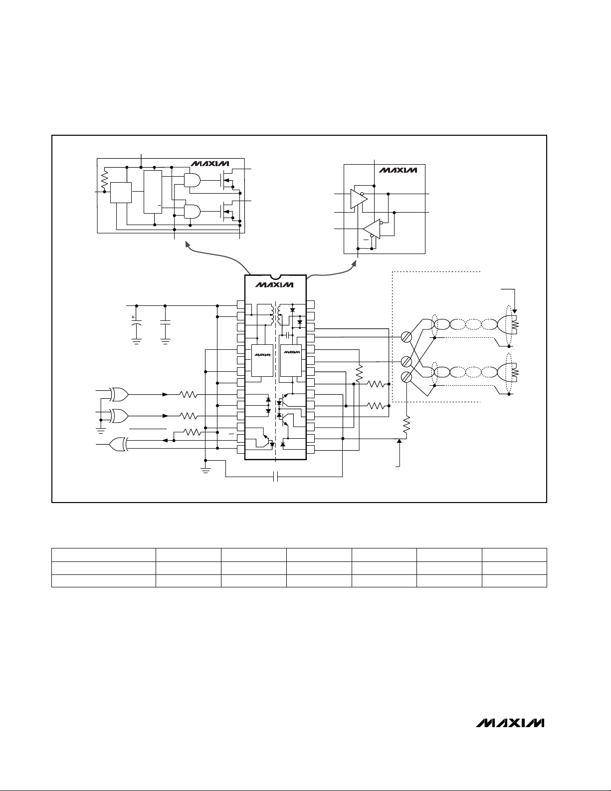
Detailed Description
The MAX1480EA/MAX1480EC/MAX1490EA/MAX1490EB
are complete, electrically isolated, RS-485/RS-422 datacommunications interface solutions. Transceivers, optocouplers, a power driver, and a transformer in one
standard 28-pin DIP package (24-pin package for the
MAX1490EA/MAX1490EB) provide a complete interface. Signals and power are internally transported
across the isolation barrier (Figures 1, 2). Power is
transferred from the logic side (nonisolated side) to the
isolated side of the barrier through a center-tapped
transformer. Signals cross the barrier through highspeed optocouplers. A single +5V supply on the logic
side powers both sides of the interface. The
MAX1480EA/MAX1480EC offer half-duplex communications while the MAX1490EA/MAX1490EB feature fullduplex communication. The functional input/output
relationships are shown in Tables 3 through 6.
The MAX1480EC/MAX1490EB feature reduced-slew-rate
drivers that minimize EMI and reduce reflections caused
by improperly terminated cables, allowing error-free
transmission at data rates up to 160kbps. The
MAX1480EA/MAX1490EA driver slew rate is not limited,
allowing transmission rates up to 2.5Mbps.
The MAX1480EC/MAX1490EB shutdown feature reduces
supply current to as low as 0.2µA by using the SD pin (see
Low-Power Shutdown Mode section).
Drivers are short-circuit current limited and are protected against excessive power dissipation by thermal
shutdown circuitry that puts the driver outputs into a
high-impedance state. The receiver input has a fail-safe
feature that guarantees a logic-high RO (logic-low RO)
output if the input is open circuit.
On the MAX1480EA/MAX1480EC, the driver outputs are
enabled by bringing DE´ high. Driver-enable time is typically 1.0µs. Allow time for the devices to be
enabled before sending data (see Typical Operating
Characteristics). When enabled, driver outputs function
as line drivers. Driver outputs are high impedance when
DE´ is low. When outputs are high impedance, they function as line receivers.
The MAX1480EA/MAX1480EC/MAX1490EA/MAX1490EB
withstand 1260V
RMS
(1min) or 1520V
RMS
(1s). The logic
inputs can be driven from TTL/CMOS logic with a series
resistor, and the received data output can directly drive
TTL or CMOS-logic families with only a resistive pullup.
Low-Power Shutdown Mode
The SD pin shuts down the oscillator on the internal power
driver. With the primary side in shutdown, no power is
transferred across the isolation barrier. The DI and DE
optocouplers, however, still consume current if the drive
signals on the nonsolated side are low. Therefore, leave
DI´ and DE´ high or floating when in shutdown mode.
Under these conditions, the MAX1480EC/MAX1490EB
supply current is reduced to as low as 0.2µA.
___________________________________________________Pin Description (continued)
Note: For DE´ and DI´ pin descriptions, see Detailed Block Diagram and Typical Application Circuit (Figure 1 for MAX1480EA/
MAX1480EC, Figure 2 for MAX1490EA/MAX1490EB).
Internal Connections. Leave these pins unconnected.
AC2, AC123, 2427, 28
26 22 ISO V
CC1
Isolated Supply Voltage Source
Inverting Driver Output and Inverting Receiver InputB—25
Isolated Receiver-Output Drive. Connect to ISO RO LED through a resistor (see
Table 1 for MAX1480EA/MAX1480EC, Table 2 for MAX1490EA/MAX1490EB).
ISO RO DRV2124
23 — A Noninverting Driver Output and Noninverting Receiver Input
Isolated Driver Input. Connect to ISO DI DRV for normal operation.ISO DI IN—22
Isolated Driver-Enable Input. Connect to ISO DE DRV for normal operation.ISO DE IN—21
Noninverting Receiver InputA20—
Inverting Receiver InputB19—
Inverting Driver OutputZ18—
Noninverting Driver OutputY17—
FUNCTIONNAME
MAX1490EA/
MAX1490EB
MAX1480EA/
MAX1480EC
PIN
Page 10
MAX1480E/MAX1490E
±15kV ESD-Protected, Isolated RS-485/RS-422
Data Interfaces
10 ______________________________________________________________________________________
The high-speed optocouplers on the MAX1480EA/
MAX1480EC/MAX1490EA consume an additional 10mA
through V
CC5(VCC4
for the MAX1490EA). Therefore, to
completely shut down these devices, use an external Pchannel MOSFET as shown in Figure 3. In normal operation, SD is low, turning the MOSFET on and thereby
providing power to all the VCCpins. When SD is pulled
high, the power oscillator is disabled and the switch is
turned off, disconnecting power from the DI and DE opto-
couplers. In normal operating mode, the switch carries
only the optocoupler currents, so an on-resistance of several ohms does not significantly degrade efficiency.
Figure 1. MAX1480EA/MAX1480EC Detailed Block Diagram and Application Circuit
Table 1. Pullup and LED Drive Resistors for Figure 1
PART R1 (Ω) R2 (Ω) R3 (Ω)
MAX1480EA
MAX1480EC
200
200
200
200
1000
3000
R4 (Ω)
4300
3000
R5 (Ω)
1000
3000
R6 (Ω)
200
200
V
CC3
V
V
GND1
V
V
GND2
V
D1
N
D2
N
GND1
CC1
1
CC2
2
3
D1
D2
4
5
FS
MAX845E
6
SD
7
CC3
8
DI
9
CC4
10
DE
11
12
RO
13
CC5
14
ISOLATION BARRIER ISOLATED COMMON
SD
C2
0.1µF
DI´
DE
MAX845E
R1*
R2*
´
R3*
Q
OSC
V
IN
+5V
DRIVER INPUT
DRIVER ENABLE
RECEIVER OUTPUT
C1
22µF
T F/F
Q
LOGIC GROUND
FS
1.07MHz/
1.45MHz
OR EQUIVALENT
DI
DE
RO
*SEE TABLE 1.
74HC86
MAX1480EA
MAX1480EC
270pF
4kV
MAX1487E
MAX487E
ISO DI IN
ISO DE IN
ISO RO DRV
AC1 (MAKE NO CONNECTION)
28
AC2 (MAKE NO CONNECTION)
27
ISO V
CC1
26
B
25
ISO RO DRV
24
A
23
ISO DI IN
22
ISO DE IN
21
ISO COM1
20
ISO DI DRV
19
ISO V
CC2
18
ISO DE DRV
17
ISO COM2
16
ISO RO LED
15
ISO V
D
RE
ISO COM1
R6*
CC1
R
R4*
R5*
MAX1480EA: MAX1487E
MAX1480EC: MAX487E
EXTERNAL RS-485/RS-422 WIRING
B
A
SH
R7
100Ω
B
A
TERMINATING RESISTOR
(ONE RESISTOR ON EACH END)
TWISTED PAIR
TO OTHER TRANSCEIVERS
SHIELD (OPTIONAL)
TWISTED PAIR
TO OTHER TRANSCEIVERS
SHIELD (OPTIONAL)
NOTE: RESISTOR R7 PROTECTS
THE MAX1480EA FROM TRANSIENT
CURRENTS BETWEEN SHIELD AND
TRANSMISSION LINES.
R
L
R
L
Page 11

MAX1480E/MAX1490E
±15kV ESD-Protected, Isolated RS-485/RS-422
Data Interfaces
______________________________________________________________________________________ 11
MAX1480EC/MAX1490EB:
Reduced EMI and Reflections
The MAX1480EC/MAX1490EB are slew-rate-limited,
minimizing EMI and reducing reflections caused by
improperly terminated cables. Figure 11 shows both
the driver output waveform of a MAX1480EA/
MAX1490EA transmitting a 150kHz signal and the
Fourier analysis of that waveform. High-frequency harmonics with large amplitudes are evident. Figure 12
shows the same information for the slew-rate-limited
MAX1480EC/MAX1490EB transmitting the same signal.
The high-frequency harmonics have much lower amplitudes, and therefore the potential for EMI is significantly
reduced.
Driver Output Protection
There are two mechanisms to prevent excessive output
current and power dissipation caused by faults or by
bus contention. A foldback current limit on the output
stage provides immediate protection against short cir-
Figure 2. MAX1490EA/MAX1490EB Detailed Block Diagram and Typical Application Circuit
Table 2. Pullup and LED Drive Resistors for Figure 2
MAX1490EB 200 3000 330 3000
10003301000200MAX1490EA
R4 (Ω)R3 (Ω)R2 (Ω)R1 (Ω)PART
FS
OR EQUIVALENT
DI
RO
*SEE TABLE 2.
V
IN
+5V
74HC86
V
CC3
OSC
1.07MHz/
1.45MHz
C1
22µF
DRIVER INPUT
RECEIVER OUTPUT
Q
T F/F
Q
SD GND1
C2
0.1µF
R1*
´
DI
R2*
LOGIC GROUND
V
CC1
V
CC2
GND1
V
V
GND2
D1
D2
FS
SD
CC3
CC4
R0
DI
MAX845
1
2
3
4
5
6
7
8
9
10
11
12
N
N
MAX1490EA/
MAX1490EB
MAX845
ISOLATION BARRIER
270 pF
4kV
D1
D2
ISO RO DRV
ISO DI DRV
AC1 (MAKE NO CONNECTION)
24
AC2 (MAKE NO CONNECTION)
23
ISO V
CC1
22
ISO RO DRV
21
A
20
B
19
MAX488E
MAX490E
Z
18
Y
17
ISO COM1
16
ISO DI DRV
15
ISO V
CC2
14
ISO RO LED
13
MAX1490EA: MAX490E
MAX1490EB: MAX488E
R3*
R
D
R5, 100Ω
R4*
R6, 100Ω
ISOLATED COMMON
A
B
Z
Y
EXTERNAL RS-485/RS-422 WIRING
TERMINATING RESISTOR
(ONE RESISTOR ON EACH END)
TWISTED PAIR
TO OTHER TRANSCEIVERS
R
A
B
Z
Y
SH1
SH2
L
SHIELD (OPTIONAL)
R
L
NOTE: RESISTORS R5 AND R6 PROTECT
THE MAX1490EA/MAX1490EB FROM
TRANSIENT CURRENTS BETWEEN SHIELD AND
TRANSMISSION LINES.
TWISTED PAIR
TO OTHER TRANSCEIVERS
SHIELD (OPTIONAL)
R
L
R
L
Page 12

MAX1480E/MAX1490E
±15kV ESD-Protected, Isolated RS-485/RS-422
Data Interfaces
12 ______________________________________________________________________________________
Figure 4. Driver DC Test Load
Figure 5. Driver/Receiver Timing Test Circuit
Test Circuits
Figure 3. MAX1480EA Low-Power Shutdown Mode
MAX1480EA
V
IN
+5V
Si9433DY
SHUTDOWN
R1
DI
´
R2
´
DE
RO
CC1
1
V
CC2
2
D1
3
D2
4
GND1
V
CC3
V
CC4
GND2
V
CC5
5
FS
6
SD
7
8
DI
9
10
DE
11
12
RO
13
14
MAX1487EMAX845
P
R3
28
27
26
25
24
23
22
21
20
19
18
17
16
15
AC1V
AC2
ISO V
CC1
B
ISO RO DRV
A
ISO DI IN
ISO DE IN
ISO COM1
ISO DI DRV
ISO V
CC2
ISO DE DRV
ISO COM2
ISO RO LED
ISOLATION BARRIER
R
D
V
OD
R
V
OC
GND
ISOLATION BARRIER
ISOLATION BARRIER
(DE´)
R
DI´
V
ID
C
L1
DIFF
C
L2
ISOLATION BARRIER
( ) ARE FOR
THE MAX1480EA/MAX1480EC.
RD
* OPTOCOUPLER
OUTPUTS. SEE FIGURES 1
AND 2 FOR DETAILED BLOCK
DIAGRAM AND TYPICAL
APPLICATION CIRCUIT.
RO (RO)*
Page 13
MAX1480E/MAX1490E
±15kV ESD-Protected, Isolated RS-485/RS-422
Data Interfaces
______________________________________________________________________________________ 13
Figure 6. Driver Timing Test Load
Figure 7. Driver Propagation Delays and Transition Times
Figure 8. Driver Enable and Disable Times
Figure 9. Times to/from Shutdown
Figure 10. Receiver Propagation Delays
Switching Waveforms
____________________________________________________Test Circuits (continued)
_
ISO V
CC
OUTPUT
500Ω
S1
UNDER TEST
C
L
S2
V
V
- 0.4V
CC_
DI´ 0
V
DIFF
- 0.4V
CC_
2
t
PLH
t
PHL
B
V
O
A
1/2 V
O
V
O
0
-V
10%
O
t
R
V
90%
= V (A) - V (B)
DIFF
t
SKEW = tPLH
- t
PHL
V
- 0.4V
t
90%
F
CC_
2
1/2 V
O
10%
V
DE´
CC_
-0.4V
A, B
V
OL
A, B
V
- 0.4V
CC_
2
0
t
ZL
2.3V
OUTPUT NORMALLY LOW
V
- 0.4V
CC_
2
t
LZ
V
+ 0.5V
OL
OUTPUT NORMALLY HIGH
V
0
2.3V
t
ZH
t
HZ
OH
- 0.5V
2.4V
SD
1.6V 1.6V
0.8V
A, B
V
A, B
t
ZL(SHDN)
2.3V
OL
OUTPUT NORMALLY LOW
OUTPUT NORMALLY HIGH
0
2.3V
t
ZH(SHDN)
t
SHDN
t
SHDN
V
V
OL
OH
+ 0.5V
- 0.5V
INPUT
MAX1490EA/MAX1490EB
OUTPUT
1.5V 1.5V
t
PLH
MAX1480EA/MAX1480EC
1.5V
t
PHL
OUTPUT
t
SKEW
VA - V
RO V
RO
V
ID
-V
B
V
V
V
0
ID
OH
OL
OH
OL
= t
1.5V
PLH - tPHL
0
t
PHL
t
PLH
Page 14

MAX1480E/MAX1490E
±15kV ESD-Protected, Isolated RS-485/RS-422
Data Interfaces
14 ______________________________________________________________________________________
cuits over the entire common-mode range (see Typical
Operating Characteristics). In addition, a thermal shut-
down circuit forces the driver outputs into a high-im
pedance state if the die temperature rises excessively.
Propagation Delay Skew
Propagation delay skew is the difference between the
low-to-high and high-to-low propagation delay. Small
driver/receiver skew times help reduce EMI and reflections by maintaining balanced differential signals.
Table 3. Transmitting
Table 4. Receiving
Table 5. Transmitting
Table 6. Receiving
1
X
INPUTS*
1
High-Z
OUTPUTS
0
High-Z
1
0
Figure 11. Driver Output Waveform and FFT Plot of
MAX1480EA/MAX1490EA Transmitting a 150kHz Signal
Figure 12. Driver Output Waveform and FFT Plot of
MAX1480EC/ MAX1490EB Transmitting a 150kHz Signal
_____________________Function Tables
Half-Duplex Devices
(MAX1480EA/MAX1480EC)
Full-Duplex Devices
(MAX1490EA/MAX1490EB)
DI´
AB
DE´
0 011
≥ +0.2V
Open
INPUTS*
0
0
VA- V
B
OUTPUT
(RO)
DE´
≤ -0.2V 10
0
0
0 1
Z Y
1 00
1
1
1
OUTPUT
(RO)
0≤ -0.2V
≥ +0.2V
Open
INPUT
(V
A
- VB)
X = Don’t care; High-Z = High impedance
* For DE
´ and DI´ pin descriptions, see Detailed Block Diagram
and Typical Application Circuit (Figure 1 for MAX1480EA/
MAX1480EC, Figure 2 for MAX1490EA/MAX1490EB).
OUTPUTS
INPUT*
(DI´
)
10dB/div
0 5MHz
500kHz/div
10dB/div
0 5MHz
500kHz/div
Page 15

MAX1480E/MAX1490E
±15kV ESD-Protected, Isolated RS-485/RS-422
Data Interfaces
______________________________________________________________________________________ 15
___________Applications Information
These E versions of the MAX1480EA/MAX1480EC/
1490EA/MAX1490EB provide extra protection against
ESD. The rugged MAX1480EA/MAX1480EC/MAX1490EA/
MAX1490EB are intended for harsh environments where
high-speed communication is important. These devices
eliminate the need for transient suppressor diodes or the
use of discrete protection components. The standard
(non-E) MAX1480A/MAX1480C/MAX1490A/MAX1490B
are recommended for applications where cost is critical.
±15kV ESD Protection
As with all Maxim devices, ESD-protection structures are
incorporated on all pins to protect against electrostatic
discharges encountered during handling and assembly.
The driver outputs and receiver inputs have extra protection against static electricity. Maxim’s engineers developed state-of-the-art structures to protect these pins
against ESD of ±15kV without damage. The ESD structures withstand high ESD in all states: normal operation,
shutdown, and powered down. After an ESD event,
Maxim’s MAX1480EA/MAX1480EC/MAX1490EA/
MAX1490EB keep working without latchup. An isolation
capacitor of 270pF 4kV should be placed between ISO
COM and logic ground for optional performance against
an ESD pulse with respect to logic ground.
ESD protection can be tested in various ways; the transmitter outputs and receiver inputs of this product family
are characterized for protection to ±15kV using the
Human Body Model.
ESD Test Conditions
The ±15kV ESD test specifications apply only to the A, B,
Y, and Z I/O pins. The test surge may be referenced to
either the ISO COM or to the nonisolated GND (Figures 1
and 2).
Human Body Model
Figure 13 shows the Human Body Model, and Figure 14
shows the current waveform it generates when discharged into low impedance. This model consists of a
100pF capacitor charged to the ESD voltage of interest,
which is then discharged into the test device through a
1.5kΩ resistor.
Machine Model
The Machine Model for ESD tests all pins using a 200pF
storage capacitor and zero discharge resistance. Its
objective is to simulate the stress caused by contact that
occurs with handling and assembly during manufacturing. All pins require this protection during manufacturing—not just inputs and outputs. Therefore, after PC
board assembly, the Machine Model is less relevant to
I/O ports.
The MAX1480EA/MAX1480EC are designed for bidirectional data communications on multipoint bus-transmission lines. The MAX1490EA/MAX1490EB are designed
for full-duplex bidirectional communications that are primarily point-to-point. Figures 15 and 16 show half-duplex
and full-duplex typical network application circuits,
respectively. To minimize reflections, terminate the line at
both ends with its characteristic impedance, and keep
stub lengths off the main line as short as possible. The
slew-rate-limited MAX1480EC/MAX1490EB are more tolerant of imperfect termination and stubs off the main line.
Layout Considerations
The MAX1480EA/MAX1480EC/MAX1490EA/MAX1490EB
pinouts enable optimal PC board layout by minimizing
interconnect lengths and crossovers:
• For maximum isolation, the “isolation barrier” should
not be breached except by the MAX1480EA/
Figure 13. Human Body ESD Test Model
Figure 14. Human Body Current Waveform
R
1MΩ
C RD
CHARGE-CURRENT
LIMIT RESISTOR
HIGH-
VOLTAGE
DC
SOURCE
C
s
100pF
1500Ω
DISCHARGE
RESISTANCE
STORAGE
CAPACITOR
DEVICE
UNDER
TEST
IP 100%
90%
AMPERES
36.8%
10%
0
0
t
RL
I
r
TIME
t
DL
CURRENT WAVEFORM
PEAK-TO-PEAK RINGING
(NOT DRAWN TO SCALE)
Page 16

MAX1480E/MAX1490E
±15kV ESD-Protected, Isolated RS-485/RS-422
Data Interfaces
16 ______________________________________________________________________________________
Figure 15. Typical Half-Duplex RS-485/RS-422 Network
TERMINATING RESISTOR
(ONE RESISTOR ON EACH END)
BA
R
D
RO
DI
DE
RERE
R
RO
DE
1
2
3
4
5
6
7
8
9
10
11
12
13
14
MAX1480EA/
MAX845E
OR EQUIVALENT
DI
DE
RO
V
IN
+5V
74HC86
C1
22µF
RECEIVER OUTPUT
C2
0.1µF
DRIVER INPUT
DRIVER ENABLE
V
CC1
V
CC2
D1
D2
GND1
FS
SD
V
R1
R2
R3
CC3
V
CC4
GND2
V
CC5
DI
DE
RO
BA
D
DI
MAX1480EC
MAX487E
MAX1487E
120Ω
100Ω
AC1 (MAKE NO CONNECTION)
28
AC2 (MAKE NO CONNECTION)
27
ISO V
CC1
26
B
25
ISO RO DRV
24
A
23
ISO DI IN
22
ISO DE IN
21
ISO COM1
20
ISO DI DRV
19
ISO V
CC2
18
ISO DE DRV
17
ISO COM2
16
ISO RO LED
15
B
A
TERMINATING RESISTOR
(ONE RESISTOR ON EACH END)
R6
R4
R5
D
R
RE
B
120Ω
A
SH
DI
DE
RO
SHIELD
(OPTIONAL)
NOTE: RESISTOR R7 PROTECTS
THE MAX1480EA/MAX1480EC
FROM TRANSIENT CURRENTS
BETWEEN SHIELD AND
TRANSMISSION LINES.
R7
100Ω
LOGIC GROUND ISOLATION BARRIER ISOLATED COMMON
270pF
4kV
Page 17

MAX1480E/MAX1490E
±15kV ESD-Protected, Isolated RS-485/RS-422
Data Interfaces
______________________________________________________________________________________ 17
MAX1480EC/MAX1490EA/MAX1490EB. Connections
and components from one side should not be located near those of the other side.
• A shield trace connected to the ground on each side
of the barrier can help intercept capacitive currents
that might otherwise couple into the signal path. In a
double-sided or multilayer board, these shield traces
should be present on all conductor layers.
• Try to maximize the width of the isolation barrier
wherever possible; a clear space of at least 0.25
inches between ground and isolated common is
suggested.
Pullup and LED Drive Resistors
The MAX1480EA/MAX1480EC/MAX1490EA/MAX1490EB
are specified and characterized using the resistor values shown in Tables 1 and 2. Altering the recommended values can degrade performance.
DI and DE are intended to be driven through a series
current-limiting resistor. Directly grounding these
pins destroys the device.
The DI and DE (MAX1480EA/MAX1480EC only) inputs
are the cathodes of LEDs whose anodes are connected
to the supply. These points are best driven by a CMOSlogic gate with a series resistor to limit the current. The
resistor values shown in Tables 1 and 2 are recommended when the 74HC86 gate or equivalent is used. These
values may need to be adjusted if a driving gate with dissimilar series resistance is used.
All pullup resistors are based on optocoupler specifications in order to optimize the devices’ data-transfer rates.
Isolated Common Connection
The isolated common may be completely floating with
respect to the logic ground and the effective network
ground. The receiver input resistors cause the isolated
common voltage to go to the mean voltage of the receiver
inputs. If using shielded cable, connect the isolated common to the shield through a 100Ω resistor. In the case of
the MAX1490EA/MAX1490EB, each shield should have its
own 100Ω resistor (Figures 1, 2, 15, and 16).
Double-Isolated RS-485 Repeater
The RS-422/RS-485 standard is specified for cable
lengths up to 4000 feet. When approaching or exceeding
the specified maximum cable length, a ground-potential
difference of several tens of volts can easily develop.
This difference can be either DC, AC, at power-line frequency, or any imaginable noise or impulse waveform. It
is typically very low impedance so that if a connection
between the two grounds is attempted, very large cur-
Figure 16. Typical Full-Duplex RS-485/RS-422 Network
CC1
1
CC2
2
D1
3
D2
4
5
FS
6
SD
7
CC3
8
DI
9
CC4
10
RO
11
12
MAX1490EA/
MAX1490EB
MAX845E
ISOLATION BARRIER
AC1 (MAKE NO CONNECTION)
24
AC2 (MAKE NO CONNECTION)
23
ISO V
CC1
22
ISO RO DRV
21
A
20
B
19
MAX488E
MAX490E
Z
18
Y
17
ISO COM1
16
ISO DI DRV
15
ISO V
CC2
14
ISO RO LED
13
270pF
4kV
V
IN
+5V
74HC86
OR EQUIVALENT
DI
RO
C1
22µF
DRIVER INPUT
RECEIVER OUTPUT
C2
0.1µF
R1
´
DI
R2
V
V
GND1
V
V
GND2
LOGIC GROUND
120Ω
120Ω
120Ω
R3
R5, 100Ω
R4
R6, 100Ω
ISOLATED COMMON
A
B
Z
Y
SH1
SH2
NOTE: RESISTORS R5 AND R6 PROTECT
THE MAX1490EA/MAX1490EB FROM TRANSIENT
CURRENTS BETWEEN SHIELD AND
TRANSMISSION LINES.
SHIELD (OPTIONAL)
120Ω
SHIELD (OPTIONAL)
Y
D
DI
Z
B
RO
R
A
Page 18

MAX1480E/MAX1490E
±15kV ESD-Protected, Isolated RS-485/RS-422
Data Interfaces
18 ______________________________________________________________________________________
rents may flow. These currents are by their nature unstable and unpredictable. In addition, they may cause noise
to be injected into sensitive instrumentation and, in
severe cases, might actually cause physical damage to
such equipment.
Figure 17 shows a half-duplex (2-wire), bidirectional,
party-line repeater system that prevents interference
and/or damage from ground-potential differences. Two
MAX1480EA/MAX1480EC isolated RS-485 transceivers
are used to isolate each of the network segments from
the electrical environment of the repeater. The
MAX1480EA/MAX1480EC also regenerate bus signals
that may have been degraded by line attenuation or dispersion.
In the idle state, both transmitters are disabled, while all
receivers in the system are enabled. If any device on the
system has information for any other device, it starts
sending its data onto the bus. Each data transmission on
the bus retriggers the one-shot, keeping the sending
transmitter enabled until there are no more transmissions. All receivers receive all data; if this is undesirable,
the protocol must allow for an address field so receivers
can ignore data not directed to them.
Each node must refrain from transmitting when data
already exists on the bus, and must resend data that is
corrupted by the collisions that inevitably occur with a
party-line system. With the repeater of Figure 17, there
might be transmitters up to 8000 feet apart. That represents more than 8µs (assuming 1ns/foot of delay) in
which two nodes could be transmitting simultaneously.
The circuit in Figure 17 can be used either directly as
shown, with the slew-rate-limited MAX1480EC, for data
transfer rates up to 160kbps, or with the MAX1480EA for
data rates up to 2.5Mbps (see Table 1 for pullup and
LED resistor values when using the MAX1480EA). If dualport isolation is not needed, one of the MAX1480EC
devices can be replaced by a MAX487E for 250kbps
applications.
Reliability
These products contain transformers, optocouplers, and
capacitors, in addition to several monolithic ICs and
diodes. As such, the reliability expectations more closely
represent those of discrete optocouplers rather than the
more robust characteristics of monolithic silicon ICs. The
reliability testing programs for these multicomponent
devices may be viewed on the Maxim website
(www.maxim-ic.com) under Technical Support,
Technical Reference, Multichip Products.
Figure 17. Double-Isolated RS-485 Repeater
+5V +5V
NETWORK SEGMENT A
3kΩ 3kΩ
200Ω
23
A
25
B
26
MAX1480EC MAX1480EC
3kΩ
19
22
17
21
24 24
15
2
10
8
14
13 1
9
11
5712
200Ω
200Ω
3kΩ
DRIVER
ENABLE
B > A
23
25
26
3kΩ
19
22
17
21
15
NETWORK SEGMENT B
A
B
200Ω
200Ω
2 8 10 14
9
11
5712
DRIVER
ENABLE
A > B
200Ω
3kΩ
2
74HC04
43 13
+5V
1000pF
51kΩ
16 15
2B Q
74HC123
AQ
1
14
13
4
CLR
311
+5V
1000pF51kΩ
7
BQ
10
74HC123
CLR
6
5
12AQ9
Page 19

±15kV ESD-Protected, Isolated RS-485/RS-422
Data Interfaces
MAX1480E/MAX1490E
Maxim cannot assume responsibility for use of any circuitry other than circuitry entirely embodied in a Maxim product. No circuit patent licenses are
implied. Maxim reserves the right to change the circuitry and specifications without notice at any time.
Maxim Integrated Products, 120 San Gabriel Drive, Sunnyvale, CA 94086 (408) 737-7600___________________ 19
© 2001 Maxim Integrated Products Printed USA is a registered trademark of Maxim Integrated Products.
Ordering Information (continued) Pin Configurations (continued)
†
Data rate for A parts is up to 2500kbps. Data rate for C parts is
up to 250kbps.
Selector Guide
PART
†
TEMP. RANGE PIN-PACKAGE
28 Wide Plastic DIP0°C to +70°C
MAX1480ECCPI
MAX1480ECEPI -40°C to +85°C 28 Wide Plastic DIP
24 Wide Plastic DIP0°C to +70°C
MAX1490EACPG
MAX1490EAEPG -40°C to +85°C 24 Wide Plastic DIP
24 Wide Plastic DIP0°C to +70°C
MAX1490EBCPG
MAX1490EBEPG -40°C to +85°C 24 Wide Plastic DIP
MAX1490EB Full 0.25 Yes
No2.5FullMAX1490EA
MAX1480EC Half 0.25 Yes
No2.5HalfMAX1480EA
SLEW-
RATE
LIMITED
DATA
RATE
(Mbps)
HALF/
FULL
DUPLEX
PART
This device is constructed using a unique set of packaging
techniques that impose a limit on the thermal profile the device
can be exposed to during board-level solder attach and
rework. Maxim recommends the use of the solder profiles recommended in the industry-standard specification, JEDEC
020A, paragraph 7.6, Table 3 for IR/VPR and Convection
Reflow processes. Preheating, per this standard, is required.
Hand or wave soldering is not recommended.
TOP VIEW
V
V
GND1
V
V
GND2
V
CC1
CC2
CC3
CC4
CC5
1
2
3
D1
D2
4
5
FS
6
SD
7
8
9
DI
10
11
DE
12
RO
13
14
MAX1480EA/
MAX1480EC
MAX845
ISOLATION BARRIER
MAX487E
MAX1487E
DIP
28
27
26
25
24
23
22
21
20
19
18
17
16
15
AC1
AC2
ISO V
CC1
B
ISO RO DRV
A
ISO DI IN
ISO DE IN
ISO COM1
ISO DI DRV
ISO V
CC2
ISO DE DRV
ISO COM2
ISO RO LED
 Loading...