

Page 1
19-5017; Rev 2; 1/11
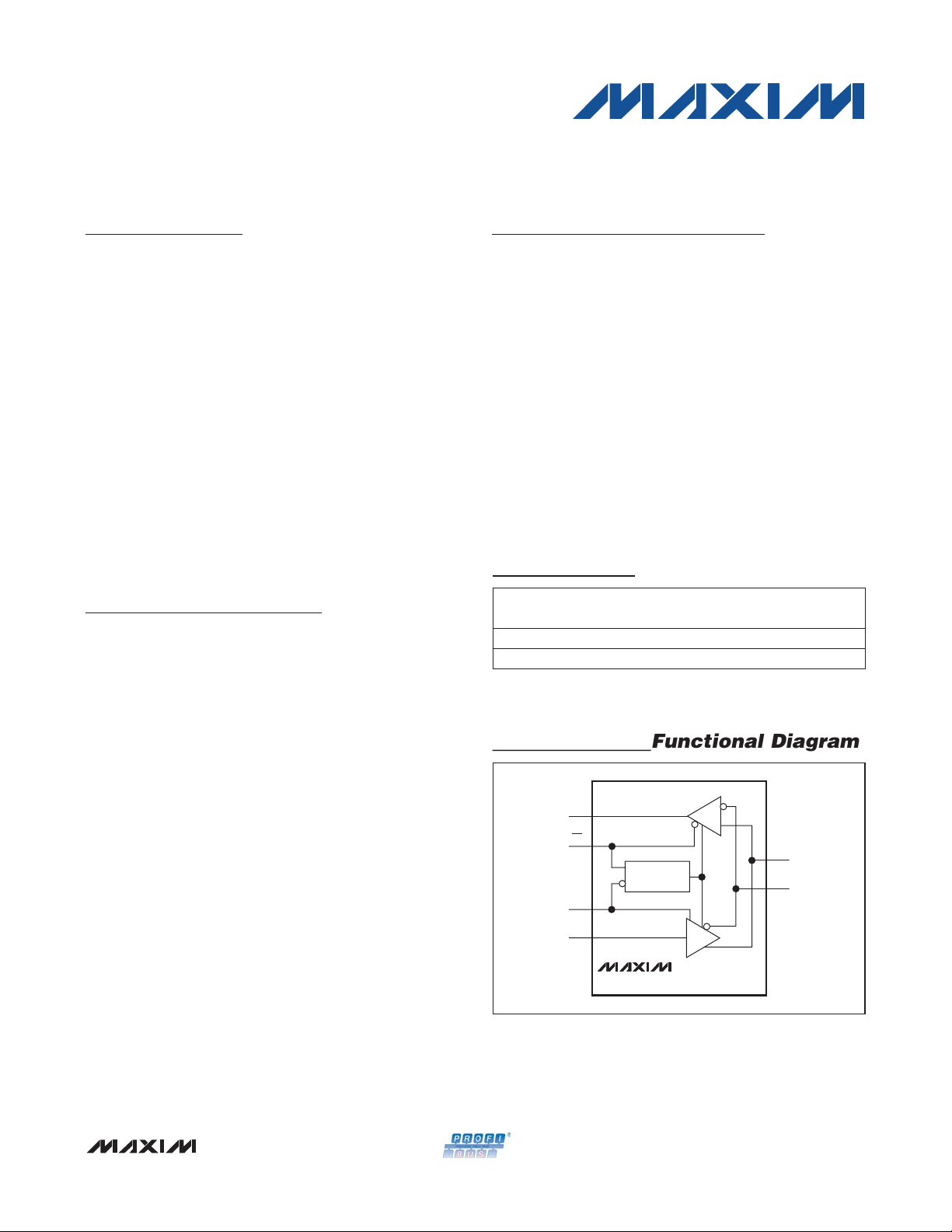
Functional Diagram
High-ESD Profibus RS-485 Transceiver
General Description
The MAX14770E is a half-duplex, Q35kV high ESDprotected transceiver for PROFIBUS-DP and RS-485
applications. In addition, it can be used for RS-422/V.11
communications. The MAX14770E is designed to meet
IEC 61158-2, TIA/EIA-422-B, TIA/EIA-485-A, V.11, and
X.27 standards.
The MAX14770E operates from a +5V supply and has
true fail-safe circuitry that guarantees a logic-high receiver output when the receiver inputs are open or shorted.
The MAX14770E features a 1/4 standard-unit load
receiver input impedance, allowing up to 128 1/4 unit
load transceivers on the bus. Drivers are short-circuit
current limited and are protected against excessive
power dissipation by thermal-shutdown circuitry.
The MAX14770E is available in 8-pin SO and tiny TDFN
(3mm x 3mm) packages, and is specified over the extended (-40NC to +85NC) and automotive (-40NC to +125NC)
temperature ranges.
Features
S Meets EIA 61158-2 Type 3 PROFIBUS-DP
S
+4.5V to +5.5V Supply Voltage
S
20Mbps Data Rate
S
Short-Circuit Protected
S
True Fail-Safe Receiver
S
Thermal-Shutdown Protected
S
Hot Swappable
S
High ESD Protection
±35kV Human Body Model (HBM)
±20kV IEC 61000-4-2 Air Gap
±10kV IEC 61000-4-2 Contact
S
-40NC to +125NC Automotive Temperature Range
in Tiny 8-Pin (3mm x 3mm) TDFN
Ordering Information
MAX14770E
Applications
PROFIBUS-DP Networks
Industrial Fieldbuses
Motion Controllers
RS-485 Networks
Machine Encoders
Typical PROFIBUS-DP Operating Circuit appears at end of
data sheet.
PART TEMP RANGE
MAX14770EESA+T
MAX14770EATA+T
+Denotes a lead(Pb)-free/RoHS-compliant package.
T = Tape and reel.
*EP = Exposed pad.
RO
RE
DE
DI
-40NC to +85NC
-40NC to +125NC
SHUTDOWN
MAX14770E
PINPACKAGE
8 SO —
8 TDFN-EP* BMG
R
A
B
D
TOP
MARK
The PROFI BUS PROCESS FIELD BUS logo is a registered
trademark of PROFIBUS and PROFINET International (PI).
_______________________________________________________________ Maxim Integrated Products 1
For pricing, delivery, and ordering information, please contact Maxim Direct at 1-888-629-4642,
or visit Maxim’s website at www.maxim-ic.com.
Page 2
High-ESD Profibus RS-485 Transceiver
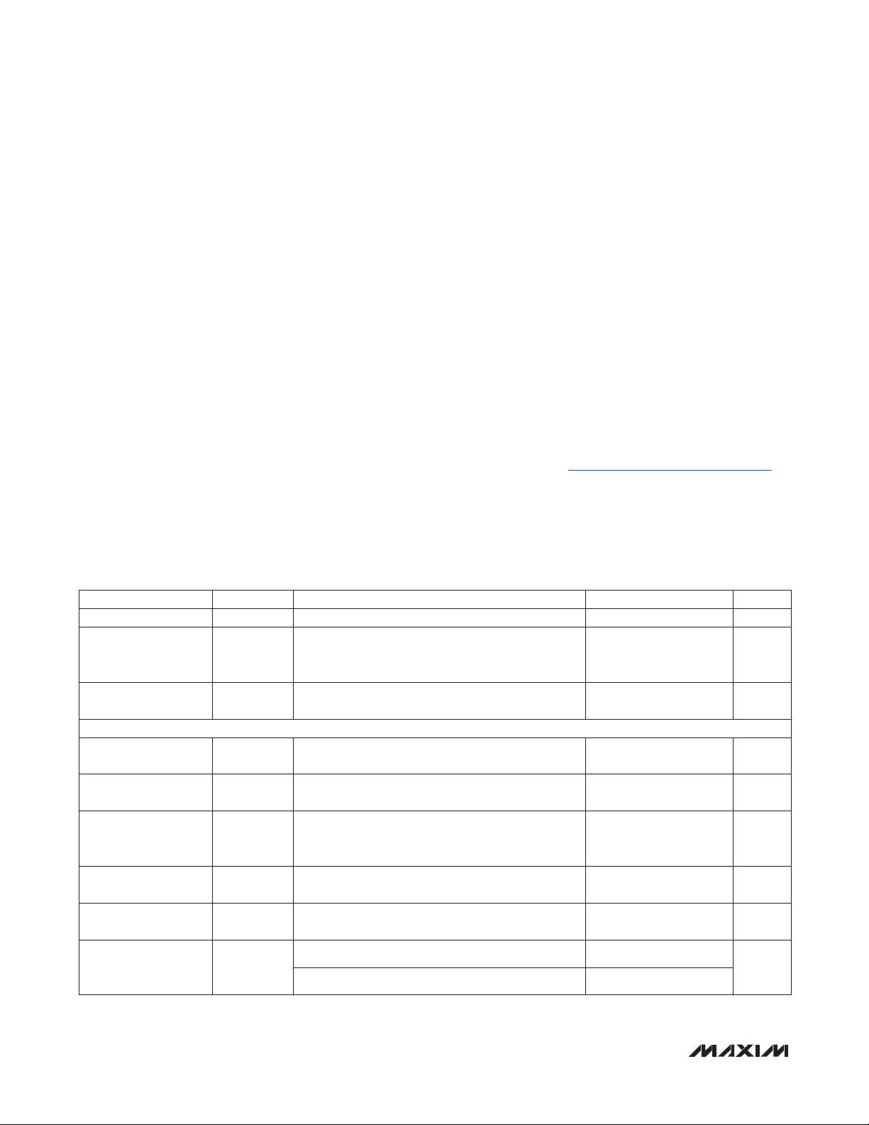
ABSOLUTE MAXIMUM RATINGS
(Voltages referenced to GND.)
V
.......................................................................-0.3V to +6.0V
CC
RE, RO .......................................................-0.3V to (V
DE, DI ...................................................................-0.3V to +6.0V
A, B .....................................................................-8.0V to +13.0V
Short-Circuit Duration (RO, A, B) to GND ................. Continuous
Continuous Power Dissipation (T
SO (derate 7.6mW/NC above +70NC) .........................606mW
TDFN (derate 24.4mW/NC above +70NC) .................1951mW
MAX14770E
PACKAGE THERMAL CHARACTERISTICS (Note 1)
SO
Junction-to-Ambient Thermal Resistance (q
Junction-to-Case Thermal Resistance (q
Note 1: Package thermal resistances were obtained using the method described in JEDEC specification JESD51-7, using a four-
layer board. For detailed information on package thermal considerations, refer to www.maxim-ic.com/thermal-tutorial.
Stresses beyond those listed under “Absolute Maximum Ratings” may cause permanent damage to the device. These are stress ratings only, and functional
operation of the device at these or any other conditions beyond those indicated in the operational sections of the specifications is not implied. Exposure to absolute
maximum rating conditions for extended periods may affect device reliability.
= +70NC)
A
JA
)...............38°C/W
JC
+ 0.3V)
CC
) ........132°C/W
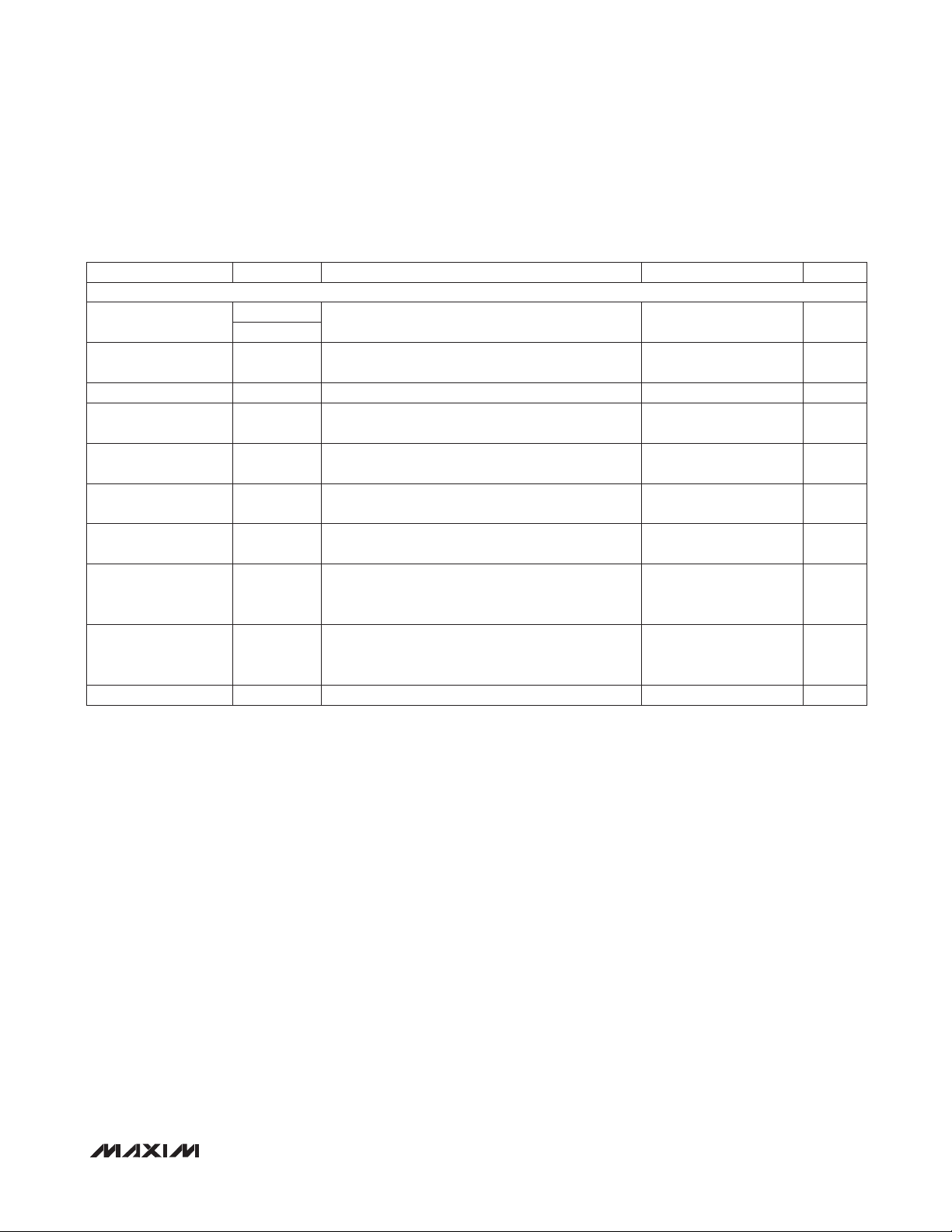
ELECTRICAL CHARACTERISTICS
(VCC = +5V Q10%, TA = T
PARAMETER SYMBOL CONDITIONS MIN TYP MAX UNITS
Power-Supply Range V
Supply Current I
Shutdown Supply
Current
DRIVER
Differential Driver
Output
Differential Driver
Peak-to-Peak Output
Change in Magnitude
of Differential Output
Voltage
Driver CommonMode Output Voltage
Change in CommonMode Voltage
Driver Short-Circuit
Output Current
(Note 5)
MIN
to T
I
|V
V
ODPP
DV
V
DV
I
OSD
, unless otherwise noted. Typical values are at VCC = +5V, T
MAX
CC
DE = 1, RE = 0 or
CC
SH
OD
OD
OC
OC
DE = 0, RE = 0 or
DE = 1, RE = 1; no load
DE = 0, RE = 1
|
= 54I, DI = VCC or GND; Figure 1
R
L
Figure 2 (Note 3) 4.0 6.8 V
RL = 54I; Figure 1 (Note 4)
RL = 54I; Figure 1
RL = 54I; Figure 1 (Note 4)
0V P V
-7V P V
P +12V; output low
OUT
P VCC; output high
OUT
Operating Temperature Range
SO .................................................................. -40NC to +85NC
TDFN ............................................................ -40NC to +125NC
Storage Temperature Range ............................ -65NC to +150NC
Junction Temperature Range ........................... -40NC to +150NC
Lead Temperature (soldering, 10s) ................................+300NC
Soldering Temperature (reflow) ......................................+260NC
TDFN
Junction-to-Ambient Thermal Resistance (q
Junction-to-Case Thermal Resistance (q
= +25NC.) (Note 2)
A
4.5 5.5 V
2.5 4 mA
2.1 V
-0.2 0 +0.2 V
1.8 3 V
-0.2 +0.2 V
-250
) ..........41°C/W
JA
).................8°C/W
JC
15
+250
FA
mA
2 ______________________________________________________________________________________
Page 3
High-ESD Profibus RS-485 Transceiver
ELECTRICAL CHARACTERISTICS (continued)
(VCC = +5V Q10%, TA = T
MIN
to T
, unless otherwise noted. Typical values are at VCC = +5V, T
MAX
PARAMETER SYMBOL CONDITIONS MIN TYP MAX UNITS
Driver Short-Circuit
Foldback Output
Current (Note 5)
I
OSDF
(VCC - 1V) P V
-7V P V
P +1V; output high
OUT
P +12V; output low
OUT
LOGIC INPUTS
Driver Input High
Voltage
Driver Input Low
Voltage
Driver Input
Hysteresis
Driver Input Current I
Input Impedance in
Hot Swap
V
V
V
R
R
IH
IL
HYS
IN
DE
RE
DE, DI, RE
DE, DI, RE
DE, DI, RE
DE, DI, RE
Figure 11 until the first low-to-high transition of DE
occurs
Figure 11 until the first high-to-low transition of RE
occurs
RECEIVER
V
Input Current (A, B) I
Differential Input
Capacitance
Receiver Differential
Threshold Voltage
Receiver Input
Hysteresis
A, IB
C
V
DV
AB
TH
TH
DE = GND, VCC = V
GND
or
+5.5V
Between A and B, DE = RE = GND at 6MHz
-7V P VCM P 12V
VCM = 0V 15 mV
= 12V +250
IN
V
= -7V -200
IN
LOGIC OUTPUT
I
Output High Voltage V
Output Low Voltage V
Three-State Receiver
Output Current
Receiver Input
Resistance
Receiver Output
Short-Circuit Current
I
OZR
R
I
OSR
OH
OL
IN
= -6mA, VA - VB = V
OUT
I
= 6mA, VA - VB = -V
OUT
0V P V
OUT
P V
CC
-7V P VCM P 12V
0V P VRO P V
CC
TH
TH
PROTECTION SPECIFICATIONS
Thermal-Shutdown
Threshold
Thermal-Shutdown
Hysteresis
ESD Protection, A
and B Pins
V
V
TS
TSH
HBM
IEC 61000-4-2 Contact Discharge to GND
= +25NC.) (Note 2)
A
-15
+15
2.0 V
0.8 V
50 mV
-1 +1
1 5.6 10
8 pF
-200 -125 -50 mV
4 V
0.4 V
-1 +1
48
-110 +110 mA
+160
15
±35
±20
±10
MAX14770E
mA
FA
kW
FA
FA
kI
NC
NC
kVIEC 61000-4-2 Air-Gap Discharge to GND
_______________________________________________________________________________________ 3
Page 4
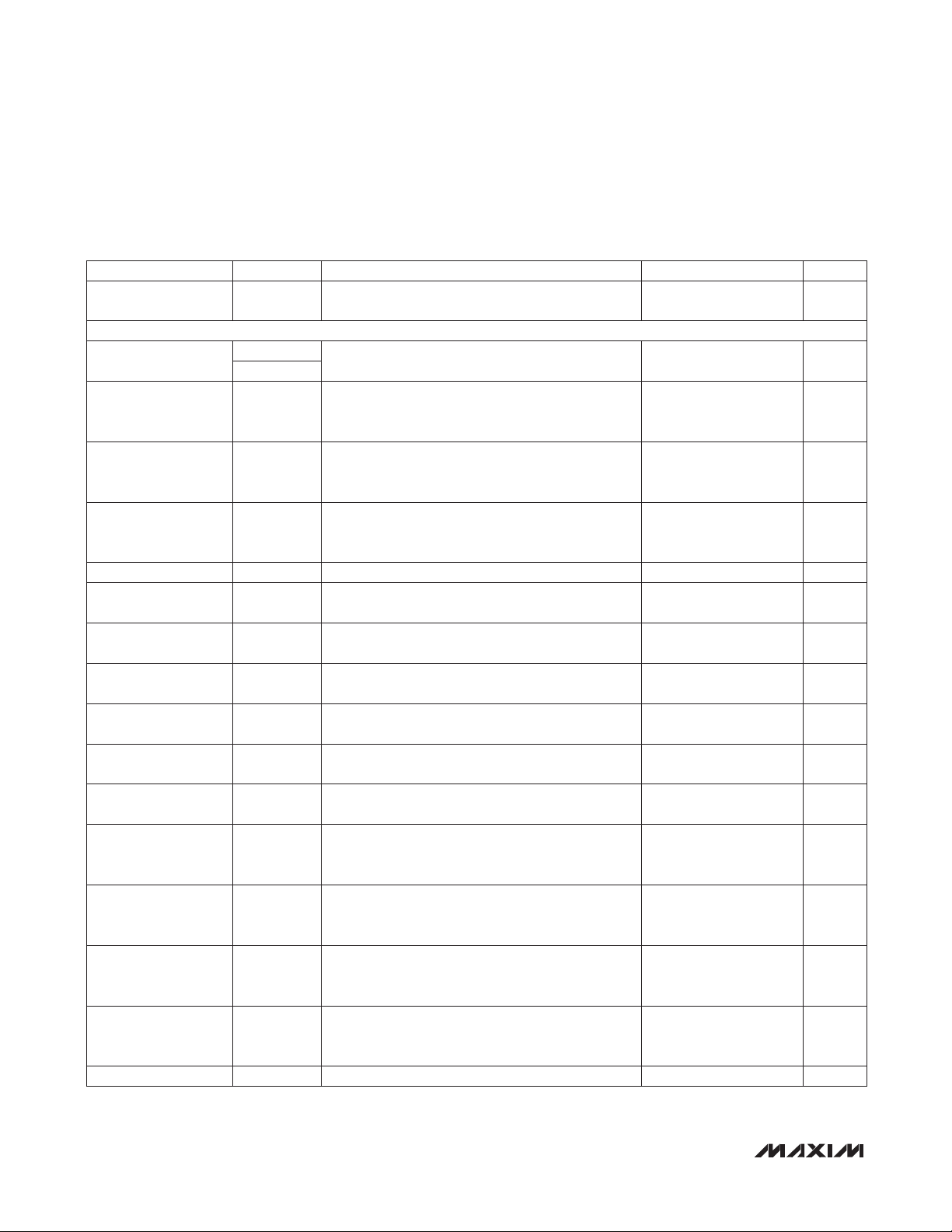
High-ESD Profibus RS-485 Transceiver
ELECTRICAL CHARACTERISTICS (continued)
(VCC = +5V Q10%, TA = T
MIN
to T
, unless otherwise noted. Typical values are at VCC = +5V, T
MAX
PARAMETER SYMBOL CONDITIONS MIN TYP MAX UNITS
ESD Protection, All
Other Pins
HBM
DRIVER SWITCHING CHARACTERISTICS
Driver Propagation
Delay
Differential Driver
MAX14770E
Output Skew |t
- t
|
DPHL
DPLH
t
DPLH
t
DPHL
t
DSKEW
RL = 54I, CL = 50pF; Figures 3 and 4
RL = 54I, CL = 50pF; Figures 3 and 4
Driver Output
Transition Skew
|t
|, |t
t(MLH)
t(MHL)
|
t
TSKEW
RL = 54I, CL = 50pF; Figures 3 and 5
Driver Differential
Output Rise or Fall
t
LH
, t
RL = 54I, CL = 50pF; Figures 3 and 4
HL
Time
Maximum Data Rate
Driver Enable to
Output High
Driver Enable to
Output Low
Driver Disable Time
from Low
Driver Disable Time
from High
Driver Enable Skew
Time
Driver Disable Skew
Time
Driver Enable High—
Propagation Delay
Difference
|t
ZL
|t
LZ
t
DZH
t
DZL
t
DLZ
t
DHZ
- tZH|
- tHZ|
t
DZH -
t
DPHL
RL = 500I, CL = 50pF; Figure 6
RL = 500I, CL = 50pF; Figure 7
RL = 500I, CL = 50pF; Figure 7
RL = 500I, CL = 50pF, Figure 6
= 500I, CL = 50pF; Figures 6 and 7
R
L
= 500I, CL = 50pF; Figures 6 and 7
R
L
Driver Enable Low—
Propagation Delay
t
DZL - tDPHL
Difference
Driver Enable from
Shutdown to Output
t
DZL(SHDN)
RL = 500I, CL = 50pF; Figure 7 (Note 6)
High
Driver Enable from
Shutdown to Output
t
DZH(SHDN)
RL = 500I, CL = 50pF; Figure 6 (Note 6)
Low
Time to Shutdown t
SHDN
(Note 6) 50 800 ns
= +25NC.) (Note 2)
A
±2
15 28 ns
1.2 ns
2 ns
7 15 ns
20 Mbps
25 48 ns
25 48 ns
20 40 ns
20 40 ns
8 20 ns
10 20 ns
46 100
46 100
kV
8 ns
8 ns
Fs
Fs
4 ______________________________________________________________________________________
Page 5
High-ESD Profibus RS-485 Transceiver
ELECTRICAL CHARACTERISTICS (continued)
(VCC = +5V Q10%, TA = T
PARAMETER SYMBOL CONDITIONS MIN TYP MAX UNITS
RECEIVER SWITCHING CHARACTERISTICS
Receiver Propagation
Delay
Receiver Output
Skew
Maximum Data Rate 20 Mbps
Receiver Enable to
Output High
Receiver Enable to
Output Low
Receiver Disable
Time from Low
Receiver Disable
Time from High
Receiver Enable from
Shutdown to Output
High
Receiver Enable from
Shutdown to Output
Low
Time to Shutdown t
Note 2: Devices are production tested at TA = +25NC. Specifications over temperature limits are guaranteed by design.
Note 3: V
Note 4: DV
Note 5: The short-circuit output current applies to peak current just prior to foldback current limiting; the short-circuit foldback out-
Note 6: Shutdown is enabled by bringing RE high and DE low. If the enable inputs are in this state for less than 50ns, the device
Note 7: Capacitive load includes test probe and fixture capacitance.
Note 8: Guaranteed by characterization; not production tested.
is the difference in VOD, with the DI at high and DI at low.
ODPP
and DVOC are the changes in |VOD| and |VOC|, respectively, with the DI at high and DI at low.
OD
put current applies during current limiting to allow a recovery from bus contention.
is guaranteed not to enter shutdown. If the enable inputs are in this state for at least 800ns, the device is guaranteed to
have entered shutdown.
to T
MIN
t
RPLH
t
RPHL
t
RSKEW
t
RZH
t
RZL
t
RLZ
t
RHZ
t
RZL(SHDN)
t
RZH(SHDN)
SHDN
, unless otherwise noted. Typical values are at VCC = +5V, T
MAX
CL = 15pF; Figures 8 and 9 (Note 7) 28 ns
CL = 15pF; Figures 8 and 9 (Notes 7, 8) 2 ns
S2 closed; RL = 1kI, CL = 15pF; Figure 10
S1 closed; RL = 1kI, CL = 15pF; Figure 10
S1 closed; RL = 1kI, CL = 15pF; Figure 10
S2 closed; RL = 1kI, CL = 15pF; Figure 10
S1 closed; RL = 1kI, CL = 15pF; Figure 10
(Notes 6, 7)
S2 closed; RL = 1kI, CL = 15pF; Figure 10
(Notes 6, 7)
(Note 6) 50 800 ns
= +25NC.) (Note 2)
A
30 ns
30 ns
30 ns
30 ns
100
100
Fs
Fs
MAX14770E
_______________________________________________________________________________________ 5
Page 6

High-ESD Profibus RS-485 Transceiver
V
CC
A
R
L
2
V
OD
V
DE
CC
A
DI
195I
110I
V
OD
MAX14770E
B
Figure 1. Driver DC Test Load
Figure 3. Driver Timing Test Circuit
V
CC
DI
0
B
R
L
V
OC
2
Figure 2. V
V
CC
DE
DI
1.5V
A
B
f = 1MHz, tLH P 3ns, t
t
DPLH
t
DPHL
R
V
ID
P 3ns
HL
Swing Under Profibus Equivalent Load Test
ODPP
L
1.5V
B
195I
C
L
1/2 V
O
A
1/2 V
O
V
O
V
O
V
0
DIFF
-V
O
20%
t
LH
80%
t
DSKEW = |tDPLH
V
DIFF
- t
= VA - V
|
DPHL
B
80%
20%
t
HL
Figure 4. Driver Propagation Delays
6 ______________________________________________________________________________________
Page 7

High-ESD Profibus RS-485 Transceiver
MAX14770E
A
t
t(MLH)
B
Figure 5. Driver Transition Skew
A
S1
50pF
C
B
GENERATOR
0 OR V
DI
CC
D
DE
50I
Figure 6. Driver Enable and Disable Times
L
50%
50%
50%
t
t(MHL)
50%
V
OUT
t
1.5V
0.25V
DHZ
R
500I
L =
DE
OUT
t
DZH
, t
DZH(SHDN)
1.5V
CC
0
V
OH
0
DE
V
CC
OUT
Figure 7. Driver Enable and Disable Times
_______________________________________________________________________________________ 7
GENERATOR
0 OR V
t
DZL
V
OL
CC
, t
DZL(SHDN)
DI
50I
1.5V
V
CC
R
500I
A
D
DE
S1
B
L =
OUT
V
CC
1.5V
t
DLZ
0
0.25V
Page 8

High-ESD Profibus RS-485 Transceiver
A
RECEIVER
ATE
Figure 8. Receiver Propagation Delay Test Circuit
V
ID
R
OUTPUT
B
MAX14770E
A
B
V
OH
RO
V
OL
Figure 9. Receiver Propagation Delays
RE
RO
+1.5V
-1.5V
t
RZH, tRZH (SHDN)
t = 1MHz, tLH P 3ns, t
t
RPHL
V
CC
2
t
RSKEW = |tRPHL
S3
V
R
ID
RE
GENERATOR
50I
V
CC
S1 OPEN
S2 CLOSED
S3 = +1.5V
0 0
V
OH
V
CC
2
0
R
1kI
RO
C
L
15pF
P 3ns
HL
t
RPLH
V
CC
2
- t
|
RPLH
S1
S2
RE
RO
t
RZL
V
, t
RZL(SHDN)
CC
1V
-1V
V
CC
S1 CLOSED
1.5V1.5V
S2 OPEN
S3 = -1.5V
V
CC
V
CC
2
V
OL
V
CC
S1 OPEN
0
V
0
OH
S2 CLOSED
S3 = +1.5V
RE
RO
0.25V
t
RLZ
RE
RO
1.5V 1.5V
t
RHZ
0.25V
Figure 10. Receiver Enable and Disable Times
8 ______________________________________________________________________________________
V
CC
0
V
CC
V
OL
S1 CLOSED
S2 OPEN
S3 = -1.5V
Page 9

High-ESD Profibus RS-485 Transceiver
SUPPLY CURRENT (mA)
Typical Operating Characteristics
(VCC = +5V, TA = +25NC, unless otherwise noted.)
MAX14770E
NO-LOAD DC SUPPLY CURRENT
vs. TEMPERATURE
2.5
2.0
1.5
1.0
0.5
NO-LOAD SUPPLY CURRENT (mA)
0
DE = V
CC
DE = GND
-40 125
TEMPERATURE (°C)
RECEIVER OUTPUT RO CURRENT
vs. OUTPUT LOW VOLTAGE
60
50
40
30
20
OUTPUT CURRENT (mA)
10
SUPPLY CURRENT
vs. DATA RATE
60
55
50
MAX14770E toc01
45
PROFIBUS EQUIVALENT LOAD
40
35
30
25
20
15
10
5
1109580655035205-10-25
0
NO LOAD
0 20,000
DATA RATE (kbps)
15,00010,0005,000
MAX14770E toc02
SHUTDOWN SUPPLY CURRENT (µA)
RECEIVER OUTPUT RO CURRENT
vs. OUTPUT HIGH VOLTAGE
60
50
MAX14770E toc04
40
30
20
OUTPUT CURRENT (mA)
10
MAX14770E toc05
RECEIVER PROPAGATION DELAY (ns)
SHUTDOWN SUPPLY CURRENT
vs. TEMPERATURE
3.0
2.5
2.0
1.5
1.0
0.5
0
-40 125
TEMPERATURE (°C)
RECEIVER PROPAGATION DELAY
vs. TEMPERATURE
25
20
15
10
5
MAX14770E toc03
1109580655035205-10-25
MAX14770E toc06
0
0 4.0
OUTPUT LOW VOLTAGE (V)
DRIVER PROPAGATION DELAY
vs. TEMPERATURE
25
RL = 54Ω, CL = 50pF
20
15
10
5
DRIVER PROPAGATION DELAY (ns)
0
-40 125
TEMPERATURE (°C)
_______________________________________________________________________________________ 9
0
3.53.02.52.01.51.00.5
1.0 5.0
OUTPUT HIGH VOLTAGE (V)
DIFFERENTIAL OUTPUT VOLTAGE V
4.54.03.53.02.52.01.5
OD
vs. OUTPUT CURRENT
4.0
3.5
MAX14770E toc07
3.0
2.5
2.0
1.5
1.0
DIFFERENTIAL OUTPUT VOLTAGE (V)
0.5
0
1109580655035205-10-25
0 80
OUTPUT CURRENT (mA)
604020
0
-40 125
TEMPERATURE (°C)
DIFFERENTIAL OUTPUT VOLTAGE V
vs. TEMPERATURE
2.8
2.7
MAX14770E toc08
2.6
2.5
2.4
2.3
2.2
2.1
DRIVER DIFFERENTIAL OUTPUT VOLTAGE (V)
2.0
-40 125
TEMPERATURE (°C)
1109580655035205-10-25
OD
RL = 54Ω
MAX14770E toc09
11095-25 -10 5 35 50 6520 80
Page 10

High-ESD Profibus RS-485 Transceiver
Typical Operating Characteristics (continued)
(VCC = +5V, TA = +25NC, unless otherwise noted.)
DRIVER OUTPUT CURRENT
vs. OUTPUT LOW VOLTAGE
140
120
100
80
MAX14770E
60
OUTPUT CURRENT (mA)
40
20
0
0 12
OUTPUT LOW VOLTAGE (V)
DRIVER OUTPUT TRANSITION SKEW
vs. TEMPERATURE
5
RL = 54Ω, CL = 50pF
4
3
2
1
DRIVER OUTPUT TRANSITION SKEW (ns)
0
-40 125
TEMPERATURE (°C)
DRIVER OUTPUT CURRENT
vs. OUTPUT HIGH VOLTAGE
140
120
MAX14770E toc10
100
80
60
OUTPUT CURRENT (mA)
40
20
0
963
-7 5
OUTPUT HIGH VOLTAGE (V)
MAX14770E toc11
31-1-3-5
DRIVER OUTPUT RISE AND FALL TIME
vs. TEMPERATURE
16
RL = 54Ω, CL = 50pF
14
MAX14770E toc13
12
10
8
TIME (ns)
6
4
2
0
1109580655035205-10-25
-40 125
TEMPERATURE (°C)
FALL TIME
MAX14770E toc14
RISE TIME
11095-25 -10 5 35 50 6520 80
DRIVER DIFFERENTIAL SKEW t
vs. TEMPERATURE
5
RL = 54Ω, CL = 50pF
4
3
2
DRIVER OUTPUT SKEW (ns)
1
0
-40 125
TEMPERATURE (°C)
DRIVER ENABLE TO
OUTPUT HIGH t
DI = VCC, RL = 500Ω, CL = 50pF
DZH
10ns/div
DSKEW
MAX14770E toc12
1109580655035205-10-25
MAX14770E toc15
DE
2V/div
A
2V/div
DRIVER ENABLE TO
OUTPUT LOW t
DI = VCC, RL = 500Ω, CL = 50pF
10ns/div
DZL
MAX14770E toc16
DE
2V/div
B
2V/div
DRIVER DISABLE TIME
FROM LOW t
DI = VCC, RL = 500Ω, CL = 50pF
10ns/div
DLZ
MAX14770E toc17
DE
2V/div
B
2V/div
DRIVER DISABLE TIME
FROM HIGH t
DI = VCC, RL = 500Ω, CL = 50pF
10 _____________________________________________________________________________________
10ns/div
DHZ
MAX14770E toc18
DE
2V/div
A
2V/div
Page 11

High-ESD Profibus RS-485 Transceiver
Pin Configurations
TOP VIEW
MAX14770E
+
RO
1
2
RE
DE
3
DI
4
MAX14770E
V
8
CC
7
B
A
6
GND
5
SO
+
1
RO
2
RE
3
DE
DI
4
MAX14770E
*EP
8
7 B
6
5
V
CC
A
GND
TDFN
(3mm × 3mm)
*CONNECT EXPOSED PAD TO GND.
Pin Description
PIN NAME FUNCTION
1 RO
2
RE
3 DE
4 DI
5 GND Ground
6 A Noninverting Receiver Input and Noninverting Driver Output
7 B Inverting Receiver Input and Inverting Driver Output
8 V
CC
— EP Exposed Pad (TDFN Only). Connect EP to GND.
Receiver Output. When RE is low and (A - B) R -50mV, RO is high; if (A - B) P -200mV, RO is low.
Receiver Enable. Drive RE low to enable RO; RO is high impedance when RE is high. Drive RE
high and DE low to enter low-power shutdown mode.
Driver Enable. Drive DE high to enable driver output. The driver outputs are high impedance when
DE is low. Drive RE high and DE low to enter low-power shutdown mode.
Driver Input. With DE high, a low on DI forces the noninverting output, A, low and the inverting output, B, high. Similarly, a high on DI forces the noninverting output, A, high and the inverting output,
B, low.
Positive Supply. Bypass VCC to GND with a 0.1FF ceramic capacitor as close as possible to the
device.
______________________________________________________________________________________ 11
Page 12

High-ESD Profibus RS-485 Transceiver
Detailed Description
The MAX14770E is a half-duplex, Q35kV high ESDprotected transceiver for PROFIBUS-DP, RS-485, and
RS-422 communications. The device features true failsafe circuitry that guarantees a logic-high receiver
output when the receiver inputs are open or shorted,
or when they are connected to a terminated transmission line with all drivers disabled (see the True Fail-Safe
section). The MAX14770E supports data rates up to
20Mbps.
MAX14770E
The MAX14770E operates from a single +4.5V to +5.5V
supply. Drivers are output short-circuit current limited. Thermal-shutdown circuitry protects drivers against
excessive power dissipation. When activated, the thermal-shutdown circuitry places the driver outputs into
a high-impedance state. The MAX14770E has a hotswap input structure that prevents disturbances on the
differential signal lines when the MAX14770E is powered
up (see the Hot-Swap Capability section).
True Fail-Safe
The MAX14770E guarantees a logic-high receiver output
when the receiver inputs are shorted or open, or when
they are connected to a terminated transmission line with
all drivers disabled. This is done by having the receiver
Table 1. Functional Table (Transmitting)
TRANSMITTING
INPUTS OUTPUTS
RE
X 1 1 0 1
X 1 0 1 0
0 0 X High-Z High-Z
1 0 X High-Z and shutdown
X = Don’t care.
DE DI B A
Table 2. Functional Table (Receiving)
RECEIVING
INPUTS OUTPUT
RE
0 X
0 X
0 X Open/shorted 1
1 1 X High-Z
1 0 X
X = Don’t care.
DE A-B RO
R -0.05V
P -0.2V
1
0
High-Z and
shutdown
threshold between -50mV and -200mV. If the differential
receiver input voltage (A - B) is greater than or equal to
-50mV, RO is logic-high. If (A - B) is less than or equal to
-200mV, RO is logic-low. In the case of a terminated bus
with all transmitters disabled, the receiver’s differential
input voltage is pulled to 0V by the termination. With
the receiver thresholds of the MAX14770E, this results
in a logic-high with a 50mV minimum noise margin. The
-50mV to -200mV threshold complies with the Q200mV
EIA/TIA-485 standard.
Hot-Swap Capability
Hot-Swap Inputs
When circuit boards are inserted into a hot or powered
backplane, disturbances to the enable inputs and differential receiver inputs can lead to data errors. Upon initial
circuit board insertion, the processor undergoes its power-up sequence. During this period, the processor output drivers are high impedance and are unable to drive
the DE and RE inputs of the MAX14770E to a defined
logic level. Leakage currents up to 10FA from the highimpedance output of a controller could cause DE and RE
to drift to an incorrect logic state. Additionally, parasitic
circuit board capacitance could cause coupling of V
CC
or GND to DE and RE. These factors could improperly
enable the driver or receiver. However, the MAX14770E
has hot-swap inputs that avoid these potential problems.
When V
rises, an internal pulldown circuit holds DE
CC
low and RE high. After the initial power-up sequence,
the pulldown circuit becomes transparent, resetting the
hot-swap-tolerable inputs.
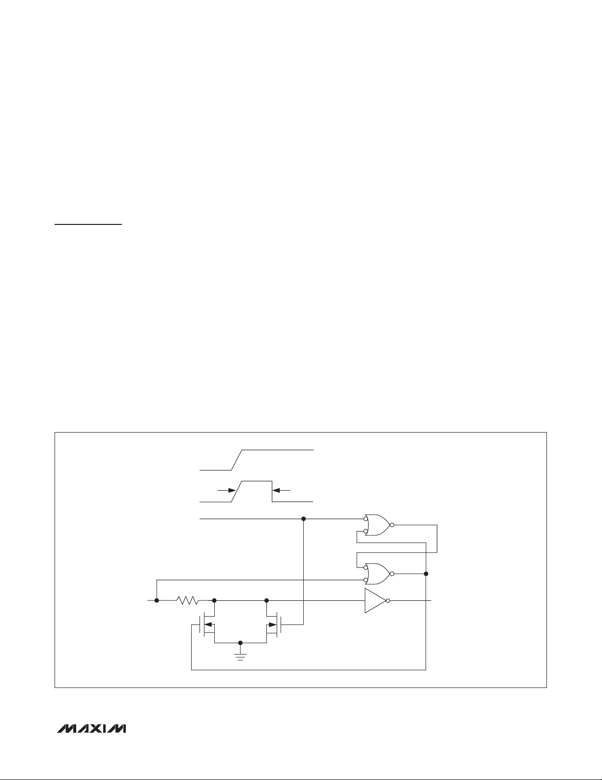
Hot-Swap Input Circuitry
The MAX14770E DE and RE enable inputs feature
hot-swap capability. At the input, there are two NMOS
devices, M1 and M2 (Figure 11). When V
ramps from
CC
0, an internal 15Fs timer turns on M2 and sets the SR
latch that also turns on M1. Transistors M2, a 1mA current sink, and M1, a 100FA current sink, pull DE to GND
through a 5.6kI resistor. M2 is designed to pull DE to
the disabled state against an external parasitic capacitance up to 100pF that can drive DE high. After 15Fs, the
timer deactivates M2 while M1 remains on, holding DE
low against three-state leakages that can drive DE high.
M1 remains on until an external source overcomes the
required input current. At this time, the SR latch resets
and M1 turns off. When M1 turns off, DE reverts to a
standard, high-impedance CMOS input. Whenever V
CC
drops below 1V, the hot-swap input is reset.
For RE, there is a complementary circuit employing two
PMOS devices pulling RE to VCC.
12 _____________________________________________________________________________________
Page 13
High-ESD Profibus RS-485 Transceiver
Thermal-Shutdown Protection
The MAX14770E features thermal-shutdown circuitry.
The internal switch turns off when the junction temperature exceeds +160NC (typ) and immediately goes into a
fault mode. The device exits thermal shutdown after the
junction temperature cools by 15NC (typ).
Applications Information
128 Transceivers on the Bus
The standard RS-485 receiver input impedance is one
unit load, and a standard driver can drive up to 32 unit
loads. The MAX14770E transceiver has a 1/4 unit load
receiver, which allows up to 128 transceivers connected
in parallel on one communication line. Connect any combination of these devices, and/or other RS-485 devices,
for a maximum of 32 unit loads to the line.
Low-Power Shutdown Mode
Low-power shutdown mode is initiated by bringing both
RE high and DE low. In shutdown, the devices draw only
15FA (max) of supply current. RE and DE can be driven
simultaneously; the devices are guaranteed not to enter
shutdown if RE is high and DE is low for less than 50ns. If
the inputs are in this state for at least 800ns, the devices
are guaranteed to enter shutdown.
Driver Output Protection
Two mechanisms prevent excessive output current and
power dissipation caused by faults or by bus contention. The first, a foldback current limit on the output
stage, provides immediate protection against short circuits over the whole common-mode voltage range (see
the Typical Operating Characteristics). The second, a
thermal-shutdown circuit, forces the driver outputs into
a high-impedance state if the die temperature exceeds
+160NC (typ).
Typical Application
The MAX14770E transceivers are designed for bidirectional
data communications on multipoint bus transmission lines.
Figure 12 shows a typical network applications circuit. To
minimize reflections, the line should be terminated at both
ends in its characteristic impedance, and stub lengths off
the main line should be kept as short as possible.
Profibus Termination
The MAX14770E is designed for driving PROFIBUS-DP
termination networks. With a worst-case loading of two
termination networks with 220I termination impedance
and 390I pullups/pulldowns, the drivers can drive
V(
> 2.1V output.
A - B)
MAX14770E
V
CC
15Fs
TIMER
TIMER
DE
Figure 11. Simplified Structure of the Driver Enable Pin (DE)
______________________________________________________________________________________ 13
5.6kI
100FA
1mA
DRIVER
ENABLE
(HOT SWAP)
M2M1
Page 14

High-ESD Profibus RS-485 Transceiver
DI
D
DE
RO
RE
MAX14770E
R
MAX14770E
B
A
Figure 12. Typical Half-Duplex RS-485 Network
R
D
1.5kI
DISCHARGE
RESISTANCE
STORAGE
CAPACITOR
CHARGE-CURRENT-
LIMIT RESISTOR
HIGH-
VOLTAGE
DC
SOURCE
R
1MI
C
100pF
C
S
120I 120I
B
A
D
DIRDE RO RE
DEVICE
UNDER
TEST
B A
DI
AMPERES
D
IP 100%
90%
36.8%
10%
R
DE RO RE
0
0
t
B
A
R
PEAK-TO-PEAK RINGING
I
R
(NOT DRAWN TO SCALE)
RL
TIME
t
DL
CURRENT WAVEFORM
DE
D
DI
RO
RE
Figure 13. Human Body ESD Test Model
Extended ESD Protection
ESD protection structures are incorporated on all pins
to protect against electrostatic discharges up to Q2kV
(HBM) encountered during handling and assembly.
A and B are further protected against high ESD up
to Q35kV (HBM) without damage. The A and B pins
Figure 14. Human Body Current Waveform
Human Body Model
Figure 13 shows the HBM. Figure 14 shows the current
waveform it generates when discharged into a lowimpedance state. This model consists of a 100pF capacitor charged to the ESD voltage of interest that is then
discharged into the device through a 1.5kI resistor.
are also protected against Q20kV Air-Gap and Q10kV
Contact IEC61000-4-2 ESD events. The ESD structures
withstand high ESD both in normal operation and when
the device is powered down. After an ESD event, the
MAX14770E continues to function without latchup.
ESD Test Conditions
ESD performance depends on a variety of conditions.
Contact Maxim for a reliability report that documents test
setup, test methodology, and test results.
14 _____________________________________________________________________________________
The IEC 61000-4-2 standard covers ESD testing and
performance of finished equipment. It does not spe-
cifically refer to integrated circuits. The MAX14770E
is specified for Q20kV Air-Gap Discharge and Q10kV
Contact Discharge IEC 61000-4-2 on the A and B pins.
The main difference between tests done using the HBM
and IEC 61000-4-2 is higher peak current in IEC 61000-4-2.
Because series resistance is lower in the IEC 61000-4-2
IEC 61000-4-2
Page 15

Typical PROFIBUS-DP Operating Circuit
R
C
50MI TO 100MI
High-ESD Profibus RS-485 Transceiver
R
330I
D
100%
90%
MAX14770E
CHARGE-CURRENT-
HIGH-
VOLTAGE
DC
SOURCE
LIMIT RESISTOR
C
150pF
S
DISCHARGE
RESISTANCE
STORAGE
CAPACITOR
Figure 15. IEC61000-4-2 ESD Test Model
V
CC
RO
RE
SHUTDOWN
DE
DI
R
A
B
D
MAX14770E
GND
390I
PROFIBUS B LINE
220I
DEVICE
UNDER
TEST
0.1FF
PROFIBUS A LINE
390I
PEAK
I
10%
= 0.7ns
t
R
TO 1ns
30ns
60ns
t
Figure 16. IEC61000-4-2 ESD Generator Current Waveform
V
R
CC
D
SHUTDOWN
DI
DE
RE
RO
0.1FF
390I
A
220I
B
390I
MAX14770E
GND
ESD test model (Figure 15), the ESD-withstand voltage
measured to this standard is generally lower than that
measured using the HBM. Figure 16 shows the current
waveform for the Q10kV IEC 61000-4-2 Level 4 ESD
Contact Discharge test. The Air-Gap Discharge test
involves approaching the device with a charged probe.
The Contact Discharge method connects the probe to
the device before the probe is energized.
Chip Information
PROCESS: BiCMOS
Package Information
For the latest package outline information and land patterns,
go to www.maxim-ic.com/packages. Note that a “+,” “#,” or
“-” in the package code indicates RoHS status only. Package
drawings may show a different suffix character, but the drawing
pertains to the package regardless of RoHS status.
PACKAGE
TYPE
8 SO S8+4
8 TDFN-EP T833+2
PACKAGE
CODE
OUTLINE
NO.
21-0041 90-0096
21-0137 90-0059
______________________________________________________________________________________ 15
LAND
PATTERN NO.
Page 16

High-ESD Profibus RS-485 Transceiver
Revision History
REVISION
NUMBER
0 10/09 Initial release —
1 4/10 Switched the position of the pins DE and DI (TDFN) in the Pin Configurations 11
2 1/11
REVISION
DATE
Updated logic output specifications, TOC 15, and the Typical PROFIBUS-DP
Operating Circuit, added the “Driver Enable High/Low—Propagation Delay
Difference” parameters and updated various typical values in the Electrical
Characteristics table
MAX14770E
DESCRIPTION
PAGES
CHANGED
3, 4, 10, 15
Maxim cannot assume responsibility for use of any circuitry other than circuitry entirely embodied in a Maxim product. No circuit patent licenses are implied.
Maxim reserves the right to change the circuitry and specifications without notice at any time.
16 Maxim Integrated Products, 120 San Gabriel Drive, Sunnyvale, CA 94086 408-737-7600
©
2011 Maxim Integrated Products Maxim is a registered trademark of Maxim Integrated Products, Inc.
 Loading...