

Page 1
19-6051; Rev 0; 9/11
MAX14759/MAX14761/MAX14763
Above- and Below-the-Rails
Low On-Resistance Analog Switches
General Description
The MAX14759/MAX14761/MAX14763 analog switches
are capable of passing bipolar signals that are beyond
their supply rails. These devices operate from a single
+3.0V to +5.5V supply and support signals in the -25V
to +25V range.
The MAX14759 is a single-pole/single-throw (SPST) analog switch, while the MAX14761 is a dual-SPST analog
switch. The MAX14763 is a single-pole/double-throw
(SPDT) analog switch.
The MAX14759 features 1I (max) on-resistance with
a Q200nA (max) on-leakage current. The MAX14761/
MAX14763 feature 2I (max) on-resistance with a Q100nA
(max) on-leakage current. The low on-resistance and
high bandwidth allow use in digital- and analog-signal
switching applications.
The MAX14759/MAX14763 are available in an 8-pin
(3mm x 3mm) TDFN package. The MAX14761 is available in a 10-pin (3mm x 3mm) TDFN package. These
devices are specified over the -40NC to +85NC extended
temperature range.
Ordering Information/Selector Guide appears at end of data
sheet.
For related parts and recommended products to use with this part, refer
to www.maxim-ic.com/MAX14759.related.
Benefits and Features
S Simplify Power-Supply Requirements
+3.0V to +5.5V Supply Range
-25V to +25V Signal Range
S High Performance
Low 1I (max) or 2I (max) On-Resistance
Low 2.4mI (typ) and 5.1mI (typ) RON Flatness
500mA (max) Switch Current for MAX14759
Thermal Shutdown Protection
-40NC to +85NC Operating Temperature Range
High Bandwidth: 100MHz (typ) Insertion Loss
High-ESD Protection Up to 2kV
S Save Board Space
Small 8-Pin and 10-Pin TDFN Packages
Applications
Industrial Measurement Systems
Instrumentation Systems
RS-485 Termination Switching
CAN Bus Termination Switching
Opto-Relay Replacement
Medical Systems
ATE Systems
Audio Signal Routing and Switching
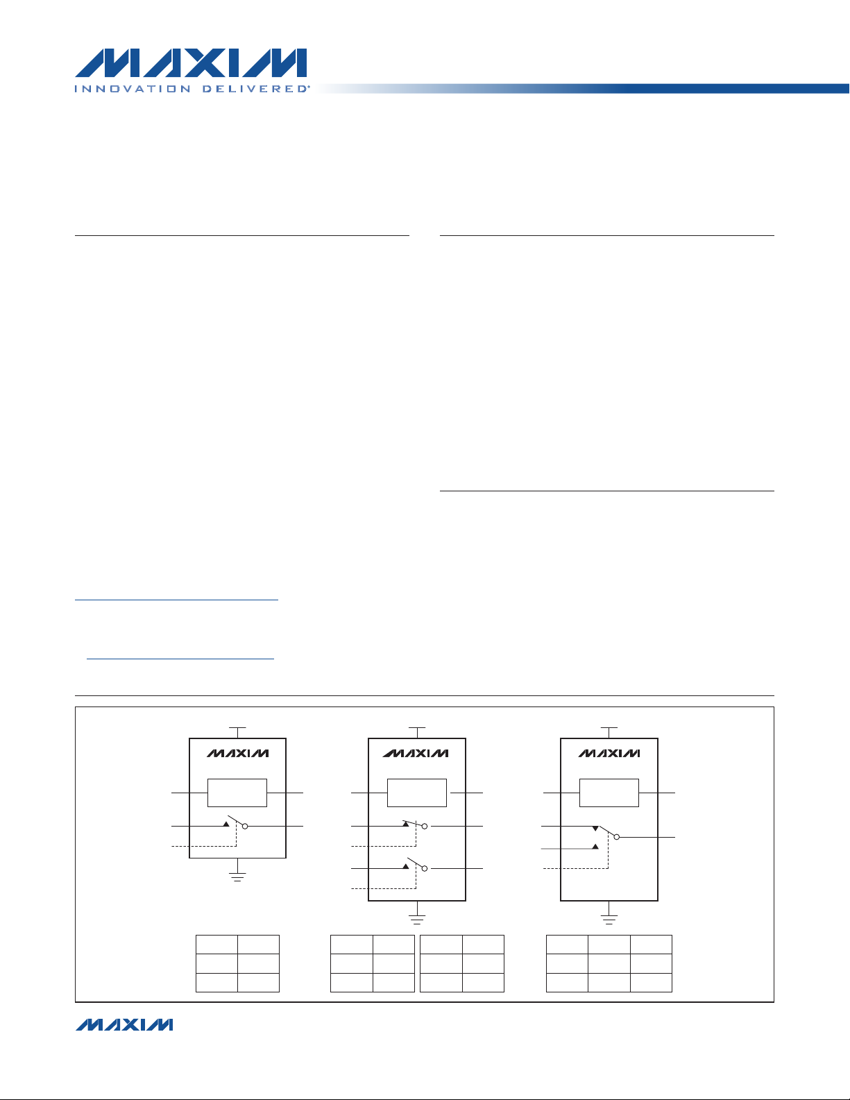
Functional Diagrams/Truth Tables
V
CC
MAX14759
OPEN
V
N
V
P
A1 B1
EN1
A2 B2
EN2
EN1 A1
0
1
V
P
AB
EN
SUPPLY
GENERATION
GND
EN A
0
1
CLOSED
����������������������������������������������������������������� Maxim Integrated Products 1
For pricing, delivery, and ordering information, please contact Maxim Direct at 1-888-629-4642,
or visit Maxim’s website at www.maxim-ic.com.
CLOSED
OPEN
V
CC
MAX14761
SUPPLY
GENERATION
GND
V
N
EN2 A2
OPEN
0
1
CLOSED
V
CC
MAX14763
V
P
A1
A2
SEL
SUPPLY
GENERATION
GND
SEL A1 A2
CLOSED OPEN
0
1
OPEN CLOSED
V
N
COM
Page 2
MAX14759/MAX14761/MAX14763
Above- and Below-the-Rails
Low On-Resistance Analog Switches
ABSOLUTE MAXIMUM RATINGS
(All voltages referenced to GND, unless otherwise noted.)
VCC .......................................................................... -0.3V to +6V
EN, EN1, EN2, SEL ...............................-0.3V to + (VCC + 0.3V)
A, B, A1, A2, B1, B2, COM .................... (VN - 0.3V) to Lesser of
(VP + 0.3V) or (VN + 52V)
VP .................................................................... -0.3V to Lesser of
(+52V) or (VN + 70V)
VN ........................Greater of (VCC - 40V) or (VP - 70V) to +0.3V
VP to V
Continuous Current Through Switch (MAX14759) ........ Q500mA
Stresses beyond those listed under “Absolute Maximum Ratings” may cause permanent damage to the device. These are stress ratings only, and functional operation of the device at these or any other conditions beyond those indicated in the operational sections of the specifications is not implied. Exposure to absolute
maximum rating conditions for extended periods may affect device reliability.
.................................................................
N
-0.3V to +70V
PACKAGE THERMAL CHARACTERISTICS (Note 1)
8-Pin TDFN
Junction-to-Ambient Thermal Resistance (qJA) ..........48°C/W
Junction-to-Case Thermal Resistance (qJC) .................8°C/W
Note 1: Package thermal resistances were obtained using the method described in JEDEC specification JESD51-7, using a four-
layer board. For detailed information on package thermal considerations, refer to www.maxim-ic.com/thermal-tutorial.
ELECTRICAL CHARACTERISTICS
(VCC = +3.0V to +5.5V, TA = -40°C to +85°C, unless otherwise noted. Typical values are at VCC = 5V and TA = +25°C.) (Note 2)
PARAMETER SYMBOL CONDITIONS MIN TYP MAX UNITS
DC CHARACTERISTICS
Power Supply Range V
Continuous Current Through
Switch
Supply Current I
Analog-Signal Range
On-Resistance R
On-Resistance Flatness
A, A1, A2 Off-Leakage Current I
COM, B, B1, B2 Off-Leakage
Current
CC
I
A_
CC
V
COM
VA_, V
ON
DR
ON
A_(OFF)
I
COM(OFF)
I
B_(OFF)
(MAX14759) -500 +500
(MAX14761/MAX14763) -250 +250
VCC ≤ 4.7V
VCC > 4.7V
,
Switch open or closed -25 +25 V
B_
IB = Q500mA, VA = Q25V (MAX14759)
I
or I
COM
(MAX14761/MAX14763)
-25V < VA < +25V, IB = Q500mA (MAX14759)
-25V < V
(MAX14761/MAX14763)
VA = +25V, VB = 0V, Figure 1 (MAX14759) -250 +250
V
= +25V, V
A_
(MAX14761/MAX14763)
V
COM
,
(MAX14759/MAX14763)
V
= 15V, V
B_
= Q250mA, VA_= Q25V
B_
< +25V, I
A_
or VB = 15V, V
Continuous Current Through Switch
(MAX14761, MAX14763) ........................................... Q250mA
Continuous Power Dissipation (TA = +70NC)
8-Pin TDFN Package
(derate 24.4mW/NC above +70NC) .........................1951.2mW
10-Pin TDFN Package
(derate 24.4mW/NC above +70NC) .........................1951.2mW
Operating Temperature Range .......................... -40NC to +85NC
Storage Temperature Range ............................ -65NC to +160NC
Lead Temperature (soldering, 10s) ................................+300NC
Soldering Temperature (reflow) ......................................+260NC
10-Pin TDFN
Junction-to-Ambient Thermal Resistance (qJA) ..........41°C/W
Junction-to-Case Thermal Resistance (qJC) .................9°C/W
3.0 5.5 V
V
= V
EN_
CC
V
= VCC/2 4.1 10
EN_
V
= V
EN_
CC
V
= VCC/2 2.5 6
EN_
or I
B_
or VB_= 0V, Figure 1
COM
A_
= 0V, Figure 1 (MAX14761) -100 +100
A_
= Q250mA
COM
= 0V, Figure 1
4.1 10
2.5 6
0.6 1
1.2 2
2.4
5.1
-250 +250
-100 +100
mA
mA
I
mI
nA
nA
����������������������������������������������������������������� Maxim Integrated Products 2
Page 3
MAX14759/MAX14761/MAX14763
Above- and Below-the-Rails
Low On-Resistance Analog Switches
ELECTRICAL CHARACTERISTICS (continued)
(VCC = +3.0V to +5.5V, TA = -40°C to +85°C, unless otherwise noted. Typical values are at VCC = 5V and TA = +25°C.) (Note 2)
PARAMETER SYMBOL CONDITIONS MIN TYP MAX UNITS
VA = ±25V, B1, B2, or COM are unconnected,
Figure 1 (MAX14759)
On-Leakage Current I
DIGITAL LOGIC
Input-Voltage Low V
Input-Voltage High V
Input Current I
AC CHARACTERISTICS
Power-On Time t
Enable Turn-On Time t
Enable Turn-Off Time t
Break-Before-Make Interval t
Off-Isolation V
Crosstalk V
-3dB Bandwidth BW
Total Harmonic Distortion Plus
Noise
Charge Injection Q V
Input Capacitance C
THERMAL PROTECTION
Thermal Shutdown Temperature t
Shutdown Temperature Hysteresis t
ESD PROTECTION
All Pins Human Body Model
Note 2: All devices are 100% production tested at TA = +25NC. Specifications over operating temperature range are guaranteed
by design.
Note 3: The power-on time is defined as the settling time for the charge pump’s output to reach steady-state value within 1%.
ON
PWRON
ON
OFF
BBM
THD+N
HYST
SHUT
VA = ±25V, B1, B2, or COM are unconnected,
Figure 1 (MAX14761)
VA = ±25V, B1, B2, or COM are unconnected,
Figure 1 (MAX14763)
VCC = 3.0V 0.7
VCC = 3.6V 0.7
IL
VCC = 4.5V 0.8
VCC = 5.5V 0.8
VCC = 3.0V 1.7
VCC = 3.6V 1.9
IH
VCC = 4.5V 2.0
VCC = 5.5V 2.1
L
V
= Q10V, CVP = CVN = 1FF, Note 3
A_
V
= Q10V, RL = 10kI, Figure 2 (MAX14759/
A_
MAX14761)
VA_ = Q10V, RL = 10kI, Figure 2 (MAX14763)
VA_ = Q10V, RL = 10kI, Figure 2
VA_ = 1V
V
= 1V
ISO
CT
IN
A_
CL = 15pF, Figure 4
RS = RL = 50I, f = 100kHz, V
Figure 5 (MAX14763)
RS = 50I, RL = 50I , V
RS = RL = 1kI, f = 20Hz to 20kHz
= GND, CL = 1nF, Figure 7 1370 pC
A_
At A, A1, A2, B, B1, B2, and COM pins 58 pF
, RL = 10kI, Figure 3 (MAX14763)
RMS
, f = 100kHz, RL = 50I,
RMS
= 1V
COM
= 1V
A_
, Figure 6
P-P
RMS
-200 +200
-100 +100
-250 +250
-1 +1 µA
320 ms
152 300
1.12 1.8 ms
300 1000
740
-77 dB
,
-83 dB
100 MHz
0.0012 %
+154
24
Q2
nA
V
V
Fs
Fs
Fs
NC
NC
kV
����������������������������������������������������������������� Maxim Integrated Products 3
Page 4
MAX14759/MAX14761/MAX14763
Above- and Below-the-Rails
Low On-Resistance Analog Switches
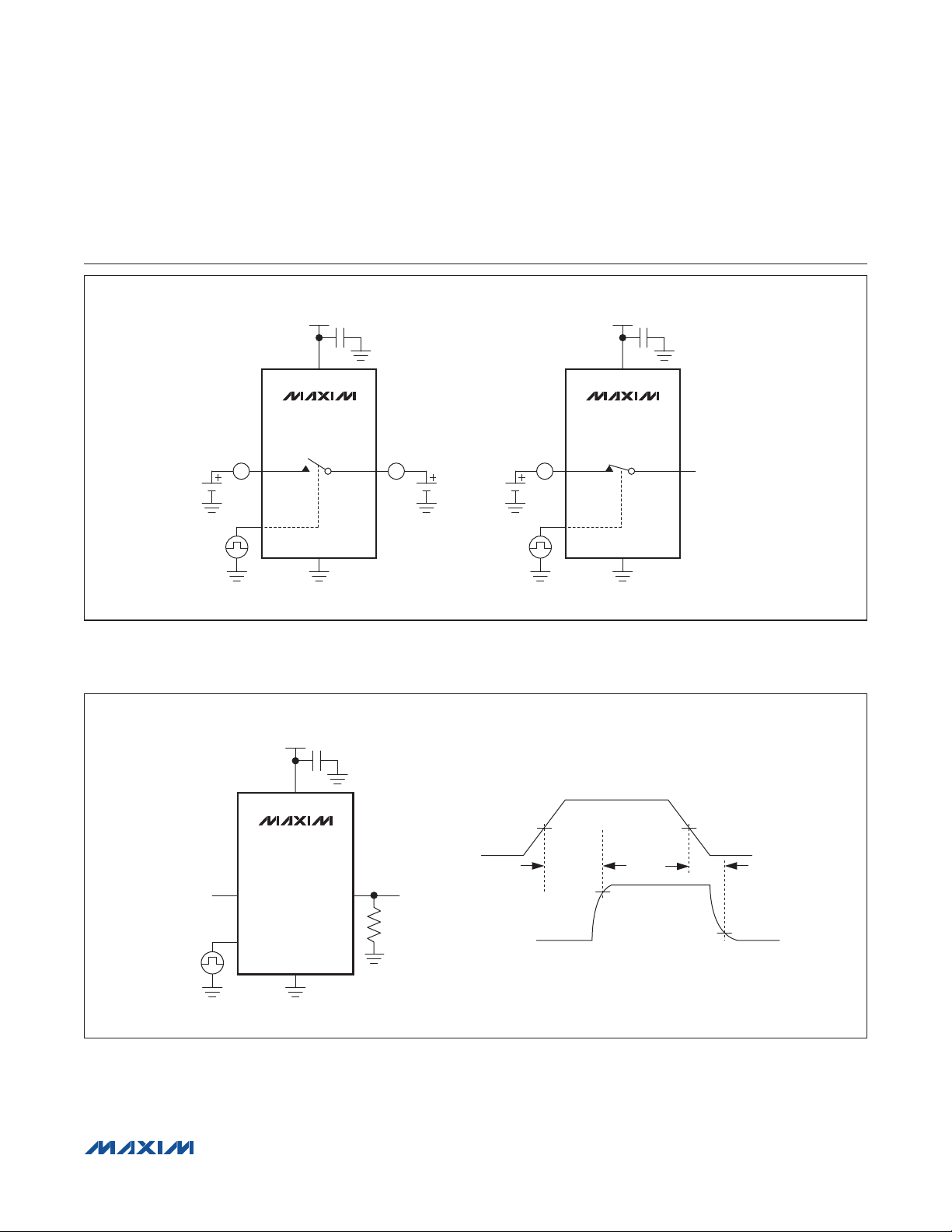
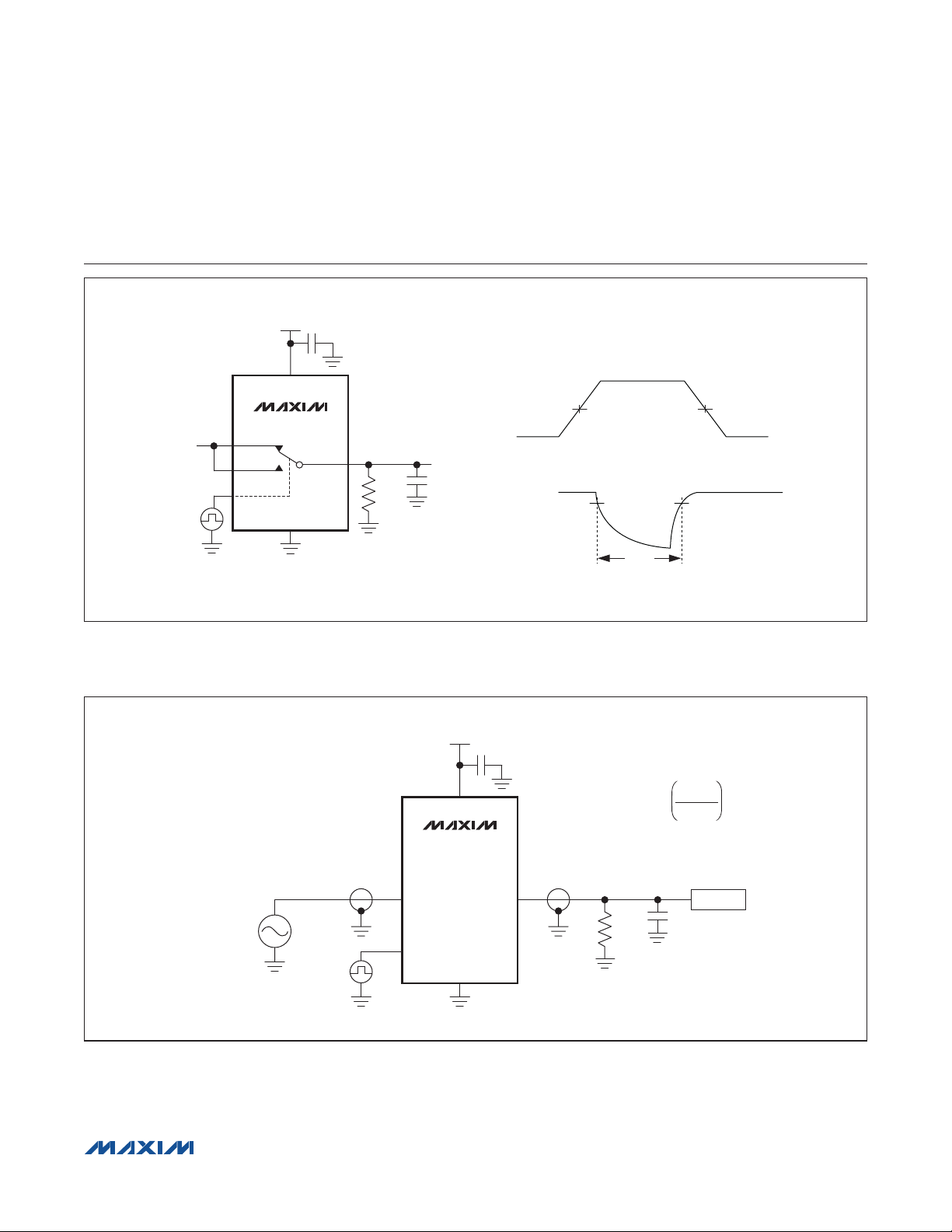
Test Circuits/Timing Diagrams
V
MAX14759
MAX14761
MAX14763
A_
EN_/SEL
SWITCH
OPEN
GND
Figure 1. Leakage Current Measurement
+5V
+5V
CC
0.1µF
0.1µF
B_/COM
+5V
0.1µF
V
CC
MAX14759
MAX14761
MAX14763
GND
B_/COM
UNCONNECTED
AA
SWITCH
CLOSED
A_
A
EN_/SEL
ON-LEAKAGE CURRENTOFF-LEAKAGE CURRENT
LOGIC
INPUT
Figure 2. Switching Time
����������������������������������������������������������������� Maxim Integrated Products 4
A_+10V
EN_/SEL
V
CC
MAX14759
MAX14761
MAX14763
GND
B_/COM V
R
L
OUT
LOGIC
INPUT
SWITCH
OUTPUT
(V
OUT
50%
0
)
t
ON
0.9 x V
OUT
50%
t
OFF
0.1 x V
OUT
Page 5
Low On-Resistance Analog Switches
+5V
0.1µF
V
CC
MAX14763
+10V
LOGIC
INPUT
CL INCLUDES FIXTURE AND STRAY CAPACITANCE.
A1
A2
SEL
COM
GND
MAX14759/MAX14761/MAX14763
Above- and Below-the-Rails
Test Circuits/Timing Diagrams (continued)
+5V
R
L
10kI
LOGIC
INPUT
0V
V
OUT
C
L
SWITCH
OUTPUT
(V
)
OUT
50%
t
BBM
0.8 x V
OUT
Figure 3. Break-Before-Make
SIGNAL
GENERATOR
Figure 4. Off-Isolation
SWITCH
OPEN
A_
EN_/SEL
+5V
V
CC
MAX14759
MAX14761
MAX14763
GND
0.1µF
B_/COM
OFF-ISOLATION = 20LOG
R
L
C
V
B_/COM
L
V
A_
ANALYZER
����������������������������������������������������������������� Maxim Integrated Products 5
Page 6

SIGNAL
GENERATOR
MAX14759/MAX14761/MAX14763
Above- and Below-the-Rails
Low On-Resistance Analog Switches
Test Circuits/Timing Diagrams (continued)
+5V
0.1µF
V
COM
CC
MAX14763
GND SEL
CROSSTALK = 20LOG
A2
A1
50I
V
COM
V
A2
ANALYZER
C
R
L
L
Figure 5. Crosstalk
+5V
Figure 6. Insertion Loss
EN_/SEL
+5V
V
CC
MAX14759
MAX14761
MAX14763
GND
0.1µF
B_/COM
V
V
IN
ON-LOSS = 20LOG
NETWORK
ANALYZER
R
MEAS
R
L
S
V
A_
IN
V
OUT
R
S
REF
R
L
V
OUT
IN
����������������������������������������������������������������� Maxim Integrated Products 6
Page 7

LOGIC
INPUT
MAX14759/MAX14761/MAX14763
Above- and Below-the-Rails
Low On-Resistance Analog Switches
Test Circuits/Timing Diagrams (continued)
+5V
0.1µF
V
A_
EN_/SEL
CC
MAX14759
MAX14761
MAX14763
GND
B_/COM
C
= 1nF
L
V
OUT
LOGIC
INPUT
SWITCH
OUTPUT
(V
OUT
+5V
OFF
0V
)
ON OFF
Q = C
L
DV
x DV
OUT
OUT
Figure 7. Charge Injection
(TA = +25°C, unless otherwise noted.)
ON-RESISTANCE vs. V
2.0
VCC = 3.3V, IB_ = 250mA (MAX14761),
1.8
= 500mA (MAX14759)
I
B
1.6
1.4
1.2
(I)
ON
R
MAX14759
1.0
0.8
0.6
0.4
0.2
-25 25
V
B_/ COM
B_/COM
MAX14761
(V)
Typical Operating Characteristics
2.0
ON-RESISTANCE vs. V
VCC = 5V, IB_ = 250mA (MAX14761),
1.8
= 500mA (MAX14759)
I
MAX14759 toc01
20155 10-15 -10 -5 0-20
B
1.6
1.4
1.2
(I)
ON
R
MAX14759
1.0
0.8
0.6
0.4
0.2
-25 25
V
COM
COM
MAX14759 toc02
MAX14761
20155 10-15 -10 -5 0-20
(V)
ON-RESISTANCE vs. TEMPERATURE
(MAX14759)
1.8
VCC = 5V, IB = 500mA
1.6
1.2
(I)
0.9
ON
R
0.6
0.3
0
-25 25
TA = +85°C
V
COM
TA = +25°C
TA = -40°C
(V)
MAX14759 toc03
20151050-5-10-15-20
����������������������������������������������������������������� Maxim Integrated Products 7
Page 8

(TA = +25°C, unless otherwise noted.)
MAX14759/MAX14761/MAX14763
Above- and Below-the-Rails
Low On-Resistance Analog Switches
Typical Operating Characteristics (continued)
ON-RESISTANCE vs. V
(MAX14761)
3.0
VCC = 5V, IB_ = 250mA
2.7
2.4
2.1
1.8
(I)
1.5
ON
R
1.2
0.9
0.6
0.3
0
-25 25
TA = +85°C
V
COM
TA = +25°C
TA = -40°C
(V)
CHARGE INJECTION vs. V
1600
MAX14759
1400
1200
1000
800
600
CHARGE INJECTION (pC)
400
200
0
-25 25
COM
TA = +25°C
20155 10-15 -10 -5 0-20
TA = +85°C
VB (V)
100
MAX14759 toc04
80
60
40
LEAKAGE CURRENT (nA)
20
0
B
TA = -40°C
LEAKAGE CURRENT vs. TEMPERATURE
(MAX14759)
OFF-LEAKAGE
-40 85
TEMPERATURE (°C)
ON-LEAKAGE
603510-15
SUPPLY CURRENT vs. TEMPERATURE
5.0
VEN = VCC (MAX14759)
4.5
MAX14759 toc07
2015-20 -15 -10 0 5-5 10
4.0
3.5
3.0
2.5
2.0
1.5
SUPPLY CURRENT (mA)
1.0
0.5
0
-40 85
51
MAX14759 toc05
41
31
21
LEAKAGE CURRENT (nA)
11
1
TEMPERATURE (°C)
LEAKAGE CURRENT vs. TEMPERATURE
(MAX14761)
OFF-LEAKAGE
ON-LEAKAGE
-40 85
TEMPERATURE (°C)
603510-15
603510-15
MAX14759 toc08
MAX14759 toc06
CROSSTALK vs. FREQUENCY
0
-20
-40
-60
CROSSTALK (dB)
-80
-100
0.01 100
FREQUENCY (MHz)
MAX14759 toc09
OFF-ISOLATION (dB)
1010.1
OFF-ISOLATION vs. FREQUENCY
0
-20
-40
-60
-80
-100
0.01 100
FREQUENCY (MHz)
1010.1
MAX14759 toc10
����������������������������������������������������������������� Maxim Integrated Products 8
Page 9

(TA = +25°C, unless otherwise noted.)
MAX14759/MAX14761/MAX14763
Above- and Below-the-Rails
Low On-Resistance Analog Switches
Typical Operating Characteristics (continued)
INSERTION LOSS vs. FREQUENCY
0
MAX14759, RL = 50I
-4
-8
-12
INSERTION LOSS (dB)
-16
-20
0.01 1000
FREQUENCY (MHz)
PSRR vs. FREQUENCY
0
-20
-40
PSRR (dB)
-60
-80
0.020
THD+N vs. FREQUENCY
0.018
MAX14759 toc11
1001010.1
MAX14759 toc13
0.016
0.014
0.012
0.010
THD+N (%)
0.008
0.006
0.004
0.002
0
0.01 100
FREQUENCY (kHz)
TURN-ON/OFF TIME vs. V
500
MAX14759
400
t
300
200
TURN-ON/OFF TIME (µs)
100
OFF
t
ON
MAX14759 toc12
1010.1
B_/COM
MAX14759 toc14
-100
0.01 100
FREQUENCY (kHz)
1010.1
0
V
(V)
B_/ COM
2015510-15 -10 -5 0-20-25 25
����������������������������������������������������������������� Maxim Integrated Products 9
Page 10

TOP VIEW
EN V
865
N.C.
MAX14759/MAX14761/MAX14763
Above- and Below-the-Rails
Low On-Resistance Analog Switches
Pin Configurations
EN1
EN2
A
P
7
10 8 7
A1 V
9
A2
P
6
SEL V
A1
P
865
7
A2
MAX14759
+
134
2
V
CC
VNBGND
*EP
MAX17461
+
2
134
V
CC
B1 V
GND B2
*EP
5
N
TDFN
*CONNECT EXPOSED PAD (EP) TO VN.
PIN
MAX14759 MAX14761 MAX14763
1 1 1 V
NAME FUNCTION
Positive-Supply Voltage Input. Bypass VCC to GND with a 0.1FF ceramic
CC
capacitor placed as close as possible to the device.
2 2 2 GND Ground
3 4 3 V
Negative Voltage Output. Bypass VN to GND with a 1FF ceramic capacitor
N
placed as close as possible to the device.
4 — — B Analog Switch Common Terminal
— — 4 COM Analog Switch Common Terminal
5 — — A Analog Switch Normally Open Terminal
6 7 6 V
Positive Voltage Output. Bypass VP to GND with a 1FF ceramic capacitor
P
placed as close as possible to the device.
7 — — N.C. No Connection. Leave unconnected.
8 — — EN
Switch Control Input. Drive EN high to close the switch or drive EN low to open
the switch.
— 8 7 A1 Analog Switch 1 Normally Closed Terminal
MAX14763
+
134
2
V
CC
VNCOMGND
Pin Description
*EP
���������������������������������������������������������������� Maxim Integrated Products 10
Page 11

MAX14759/MAX14761/MAX14763
Above- and Below-the-Rails
Low On-Resistance Analog Switches
Pin Description (continued)
PIN
MAX14759 MAX14761 MAX14763
— 3 — B1 Analog Switch 1 Common Terminal
— 6 5 A2 Analog Switch 2 Normally Open Terminal
— 5 — B2 Analog Switch 2 Common Terminal
— 10 — EN1
— 9 — EN2
— — 8 SEL
— — — EP
NAME FUNCTION
Switch 1 Control Input. Drive EN1 high to open switch 1 or drive EN1 low to
close switch 1.
Switch 2 Control Input. Drive EN2 high to close switch 2 or drive EN2 low to
open switch 2.
Switch Control Input. Drive SEL low to connect the COM terminal to A1 or drive
SEL high to connect the COM terminal to A2.
Exposed Pad. Internally connected to VN; not intended as an electrical
connection. Leave exposed pad unconnected.
Detailed Description
The MAX14759/MAX14761/MAX14763 are analog switches
capable of handling signals above and below their rails.
These devices operate from a single +3.0V to +5.5V supply and support signals in the -25V to +25V range. The
low on-resistance and high bandwidth allow for use in
digital- and analog-signal switching applications.
Analog Signal Range
The devices switch signals in the range from -25V to +25V
that are above and below their rails. The on-resistance for
these devices exhibit a high degree of flatness of 2.4mI
(MAX14759 typ) and 5.1mI (MAX14761/MAX14763 typ)
over the whole input voltage range of -25V to +25V. The
analog switches allow bidirectional current flow, so A, A1,
A2, B, B1, B2, and COM can be used as either inputs or
outputs.
Bypass Capacitors
Bias stabilizing capacitors are required on the VP and VN
pins. 1FF ceramic capacitors are suggested for effective
operation. VP and VN are not intended as a power supply
for other circuitry.
Ensure that negative signals are not present on the A_,
B_, or COM inputs until 1 second has passed after applying VCC.
Differential Termination Resistor Switch
The MAX14759 can be used to switch a differential termination resistor in or out. In RS-485 and CAN applications,
both ends of high-speed transmission lines require termination. Figures 8 and 9 show an application of RS-485
and CAN termination using two equal resistors. These
switches support RS-485’s high -7V to +12V commonmode range.
In RS-232/RS-485 multiprotocol applications, the
MAX14759 can be used for switching in the line-terminating resistors for RS-485 usage, and can disable the
termination resistor for RS-232 operation, as shown in
Figure 10.
The MAX14761 is ideal for switching in fail-safe biasing
resistors in RS-485 applications, as shown in Figures 11
and 12.
Applications Information
Power-Up Conditions
���������������������������������������������������������������� Maxim Integrated Products 11
Page 12

Figure 8. RS-485 Termination Switch
MAX14759/MAX14761/MAX14763
Above- and Below-the-Rails
Low On-Resistance Analog Switches
V
CC
A
RT/2
A
MAX14840
GND
TERMINATION
CONTROL
EN
MAX14759
B
R
/2
T
CANH
RT/2
A
EN EN
CANL
CTRL
B
R
T
MAX3051
Figure 9. CAN Termination Switch
MAX14759
/2
V
CC
MAX3160
RS-485/
RS-232
GND
RT/2
A
MAX14759
B
/2
R
T
A
RT/2
A
EN
CONTROL
B
MAX14759
B
/2
R
T
CTRL
MAX3051
Figure 10. Multiprotocol Termination Switch
���������������������������������������������������������������� Maxim Integrated Products 12
Page 13

MAX14759/MAX14761/MAX14763
Above- and Below-the-Rails
Low On-Resistance Analog Switches
V
CC
R
PU
A1
MAX14761
R
T
RS-485
TRANSCEIVER
Figure 11. Pullup and Pulldown Resistance Switch
V
CC
RS-485
TRANSCEIVER
CONTROL
EN1
EN2
EN1B1
EN2B2
A2
R
PD
A1
MAX14761
A2
B1
B2
CONTROL
V
CC
R
PU
R
T
GND
Figure 12. Fail-Safe Biasing Network Switch
���������������������������������������������������������������� Maxim Integrated Products 13
R
PD
Page 14

MAX14759/MAX14761/MAX14763
Above- and Below-the-Rails
Low On-Resistance Analog Switches
MAX14763
AUDIO
AMPLIFIER
2
AUDIO
AMPLIFIER
1
CONTROL
AUDIO
AMPLIFIER 1
AUDIO
AMPLIFIER 2
MAX14763
A1
COM
A2
SEL
CONTROL
Figure 13. Single-Ended Amplifier Switching Figure 14. Differential Amplifier Switching
A1
A2
SEL
A1
A2
SEL
MAX14763
COM
COM
Audio Amplifier Switch
The MAX14763 is used for selecting between audio
amplifier sources to drive loudspeaker applications
(Figures 13 and 14.)
���������������������������������������������������������������� Maxim Integrated Products 14
Page 15

MAX14759/MAX14761/MAX14763
Above- and Below-the-Rails
Low On-Resistance Analog Switches
Ordering Information/Selector Guide
PART TEMP RANGE PIN-PACKAGE FUNCTION
MAX14759ETA+
MAX14761ETB+
MAX14763ETA+
+Denotes a lead(Pb)-free/RoHS-compliant package.
*EP = Exposed pad.
-40NC to +85NC
-40NC to +85NC
-40NC to +85NC
Chip Information
PROCESS: BiCMOS
RON (MAX) (I)
8 TDFN-EP* 1 x SPST 1
10 TDFN-EP* 2 x SPST 2
8 TDFN-EP* 1 x SPDT 2
Package Information
For the latest package outline information and land patterns
(footprints), go to www.maxim-ic.com/packages. Note that a
“+”, “#”, or “-” in the package code indicates RoHS status only.
Package drawings may show a different suffix character, but
the drawing pertains to the package regardless of RoHS status.
PACKAGE
TYPE
8 TDFN T833+2
10 TDFN T1033+1
PACKAGE
CODE
OUTLINE
NO.
21-0137 90-0059
21-0137 90-0003
LAND PATTERN
NO.
���������������������������������������������������������������� Maxim Integrated Products 15
Page 16

MAX14759/MAX14761/MAX14763
Above- and Below-the-Rails
Low On-Resistance Analog Switches
Revision History
REVISION
NUMBER
0 9/11 Initial release —
REVISION
DATE
DESCRIPTION
PAGES
CHANGED
Maxim cannot assume responsibility for use of any circuitry other than circuitry entirely embodied in a Maxim product. No circuit patent licenses are implied.
Maxim reserves the right to change the circuitry and specifications without notice at any time. The parametric values (min and max limits) shown in the Electrical
Characteristics table are guaranteed. Other parametric values quoted in this data sheet are provided for guidance.
Maxim Integrated Products, 120 San Gabriel Drive, Sunnyvale, CA 94086 408-737-7600 16
©
2011 Maxim Integrated Products Maxim is a registered trademark of Maxim Integrated Products, Inc.
 Loading...