

Page 1
General Description
The MAX14752/MAX14753 are 8-to-1 and dual 4-to-1
high-voltage analog multiplexers. Both devices feature
60Ω (typ) on-resistance with 0.03Ω (typ) on-resistance
flatness. These low on-resistance multiplexers conduct
equally well in either direction. Flexible logic levels for
the channel-select interface are defined by the EN input.
The MAX14752 is a 8-to-1 multiplexer and MAX14753 is
a dual 4-to-1 multiplexer. Both devices operate with
dual supplies of ±10V to ±36V, or a single supply of
+20V to +72V.
The MAX14752/MAX14753 are available in a 16-pin
TSSOP package and are pin compatible with the industry-standard DG408/DG409. Both the MAX14752/
MAX14753 are specified over the extended -40°C to
+85°C operating temperature range.
Applications
Programmable-Logic Controllers
Environment Control Systems
ATE Systems
Medical Monitoring Systems
Automotive
Features
♦ Wide Dual Power-Supply Range ±36V (max)
♦ Wide Single Power-Supply Range +72V (max)
♦ Low On-Resistance 60Ω (typ)
♦ R
ON
Flatness Over Common-Mode Voltage 0.03Ω
(typ)
♦ Low-Input (20nA) On-Leakage Current (max)
♦ EN Voltage Defines Logic Level of S0, S1, and S2
♦ Low I
DD
Supply Current in Disable Mode 25µA (max)
♦ Overvoltage/Undervoltage Clamp Through
Protection Diodes
♦ Break-Before-Make Operation
♦ Pin Compatible with Industry-Standard
DG408/DG409
MAX14752/MAX14753
8-Channel/Dual 4-Channel
72V Analog Multiplexers
________________________________________________________________
Maxim Integrated Products
1
19-4255; Rev 3; 7/10
Ordering Information
+
Denotes a lead(Pb)-free/RoHS-compliant package.
For pricing, delivery, and ordering information, please contact Maxim Direct at 1-888-629-4642,
or visit Maxim's website at www.maxim-ic.com.
Pin Configurations appear at end of data sheet.
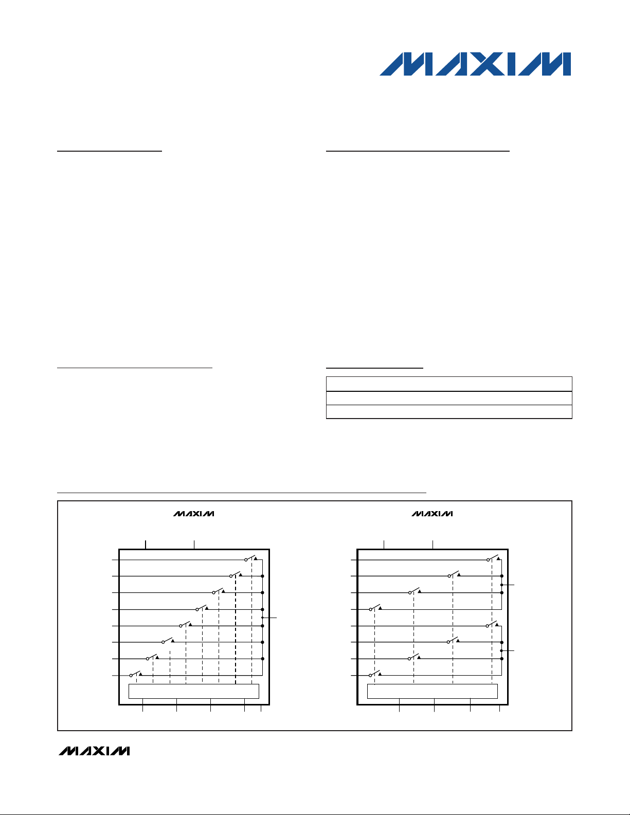
Functional Diagrams
PART TEMP RANGE PIN-PACKAGE
MAX14752EUE+ -40°C to +85°C 16 TSSOP
MAX14753EUE+ -40°C to +85°C 16 TSSOP
MAX14752
V
SS
CONTROL
S1S0 S2
EN
IN0
IN1
IN2
IN3
IN4
IN5
IN6
IN7
V
DD
GND
OUT
INA0
INA1
INA2
INA3
INB0
INB1
INB2
INB3
V
DD
S1 S0
MAX14753
V
SS
OUTA
OUTB
CONTROL
GND
EN
Page 2
MAX14752/MAX14753
8-Channel/Dual 4-Channel
72V Analog Multiplexers
2 _______________________________________________________________________________________
ABSOLUTE MAXIMUM RATINGS
Stresses beyond those listed under “Absolute Maximum Ratings” may cause permanent damage to the device. These are stress ratings only, and functional
operation of the device at these or any other conditions beyond those indicated in the operational sections of the specifications is not implied. Exposure to
absolute maximum rating conditions for extended periods may affect device reliability.
VDDto VSS.............................................................-0.3V to +72V
GND to V
SS
..............................................................-0.3V to V
DD
EN, S0, S1, S2 to GND .................................................................
..............................-0.3V to the lesser of (+12V and V
DD
+ 0.3V)
IN_, INA_, INB_, OUT, OUTA, OUTB to V
SS ......................................
...........
-2V to (V
DD
- V
SS
+ 2V) or 100mA (whichever occurs first)
Continuous Current into IN_, INA_,
INB_, OUT, OUTA, OUTB .............................................100mA
Continuous Power Dissipation (T
A
= +70°C)
16-Pin TSSOP (derate 11.1mW/°C above +70°C) ......890mW
Junction-to-Ambient Thermal Resistance (θ
JA
) (Note 1)
16-Pin TSSOP ..............................................................90°C/W
Junction-to-Case Thermal Resistance (θ
JC
) (Note 1)
16-Pin TSSOP ..............................................................27°C/W
Maximum Operating Temperature Range.........-40°C to +125°C
Junction Temperature..................................................... +150°C
Storage Temperature Range .............................-65°C to +150°C
Lead Temperature (soldering, 10s) .................................+300°C
Soldering Temperature (reflow) .......................................+260°C
DC ELECTRICAL CHARACTERISTICS–DUAL SUPPLIES
(VDD= +35V, VSS= -35V, V
GND
= 0V, VEN= +3.3V, TA= -40°C to +85°C, unless otherwise noted. Typical values are at TA= +25°C.)
)
Note 1: Package thermal resistances were obtained using the method described in JEDEC specification JESD51-7, using a four-layer
board. For detailed information on package thermal considerations, refer to www.maxim-ic.com/thermal-tutorial
.
PARAMETER SYMBOL CONDITIONS MIN TYP MAX UNITS
POWER SUPPLY
VDD Supply Voltage Range V
VSS Supply Voltage Range V
VDD Supply Current
VSS Supply Current
ANALOG MUX
Analog Signal Range
Current Through Multiplexer
On-Resistance R
On-Resistance Matching
Between Channels
On-Resistance Flatness R
Output On-Leakage Current I
DD
SS
I
DD(OFF)
I
DD(ON)
I
SS(OFF)
I
SS(ON)
, V
V
IN_
INA_,
V
, V
INB_
V
OUT,
OUTA, VOUTB
I
IN_, IINA_,
I
INB_
ON
ΔR
ON
FLAT_(ON
OUT(ON)
V
= V
E N
= 0V , V
S _
I N _ = V I N A _
= V
VEN = +5V, VS_ = 0V or VEN, V
V
= +20V
INB_
V
= V
E N
= 0V , V
S _
I N _ = V I N A _
= V
VEN = +5V, VS_ = 0V or VEN, V
= +20V
V
INB_
V
, V
, V
IN_
INA_
I
IN_, IINA_, IINB_
, V
V
OUT
OUTA
I
IN_, IINA_, IINB_
= ±20V -5 +5 mA
INB_
= 5mA; V
, V
OUTB
= 5mA, V
, V
IN_
= ±20V, Figure 1
, V
IN_
±20V, 0V
I
IN_, IINA_, IINB_
, V
V
OUT
MAX14752: V
, V
V
IN_
INA_
MAX14753: V
, V
V
IN_
INA_
OUTA
, V
, V
, V
OUT
INB_
OUT
INB_
= 5mA, V
OUTB
IN_
= ±20V
, V
, V
OUTA
= unconnected, Figure 2
, V
, V
OUTA
= unconnected, Figure 2
, V
OUTB
OUTB
= + 20V 12 25
I N B _
IN_ = VINA_
= + 20V 11 25
I N B _
IN_ = VINA_
, V
INA_
INB_
, V
INA_
INB_
, V
INA_
INB_
= ±20V,
= ±20V,
+10 +36 V
-10 -36 V
=
=
V
SS
,
=
,
-20 +20
-10 +10
270 600
260 600
V
DD
60 130 Ω
0.5 Ω
0.03 Ω
µA
µA
V
nA
Page 3
MAX14752/MAX14753
8-Channel/Dual 4-Channel
72V Analog Multiplexers
_______________________________________________________________________________________ 3
DC ELECTRICAL CHARACTERISTICS–DUAL SUPPLIES (continued)
(VDD= +35V, VSS= -35V, V
GND
= 0V, VEN= +3.3V, TA= -40°C to +85°C, unless otherwise noted. Typical values are at TA= +25°C.)
PARAMETER SYMBOL CONDITIONS MIN TYP MAX UNITS
Output Off-Leakage Current I
Input Off-Leakage Current I
LOGIC (EN, S0, S1, S2)
EN Input Voltage Low V
EN Input Voltage High V
EN, S_ Input Voltage Range VEN, VS_ 11 V
EN Input Current I
S0, S1, S2 Input Voltage Low V
S0, S1, S2 Input Voltage High V
DYNAMIC CHARACTERISTICS
Enable Turn-On Time t
Enable Turn-Off Time t
Transition Time t
Break-Before-Make Time Delay t
Frequency Response BW RS = 50Ω, RL = 1kΩ, Figure 7 20 MHz
Off-Isolation V
Crosstalk V
Total Harmonic Distortion Plus
Noise
Charge Injection Q
OUT(OFF)
IN(OFF)
EN_IL
EN_IH
EN_IH(DC)
IL
IH
ON
OFF
TRANS
BBM
ISO
CT
THD+N R
MAX14752: V
, V
V
IN_
INA_
MAX14753: V
, V
V
IN_
INA_
, V
V
OUT
OUTA
= ±20V, Figure 3
V
INB_
V
= + 11V , V
E N
or ( 0.75 x V
V
, V
IN0
INA0
V
, V
IN0
INA0
V
, V
IN0
INA0
V
, V
I N _
I N A _
Fi g ur e 6
V
, V
IN_
INA_
= 50Ω, CL = 15pF, Figure 8
R
L
RS = RL = 50Ω, Figure 9 62 dB
= RL = 1kΩ, f = 20Hz to 20kHz 0.0014 %
S
V
, V
IN_
INA_
Figure 10
, V
, V
, V
OUTB
OUTB
= ±20V,
= ±40V,
, V
IN_
INA_
-20 +20
-10 +10
,
-5 +5 nA
OUT
, V
= -20V, Figure 3
INB_
, V
OUT
, V
= -40V, Figure 3
INB_
, V
OUTB
OUTA
OUTA
= ±20V, V
0.8 V
2.1 V
= V
= V
E N
S 0
S 1
= ( 0.25 x V
S 2
)
E N
)
0.4 mA
0.25 x
V
EN
0.75 x
V
EN
= ±10V, RL = 10kΩ, Figure 4 1 25 µs
= ±10V, RL = 10kΩ , Fi g ur e 4 0.8 2 µs
= ±10V, RL = 10kΩ , Fi g ur e 5 10 µs
, V
= ± 10V , RL = 10kΩ ,
I N B _
= 1V
, V
INB_
, V
= GND, CL = 1nF,
INB_
, f = 100kHz,
RMS
10 µs
65 dB
200 pC
nA
V
V
Page 4
MAX14752/MAX14753
8-Channel/Dual 4-Channel
72V Analog Multiplexers
4 _______________________________________________________________________________________
DC ELECTRICAL CHARACTERISTICS–SINGLE SUPPLY
(VDD= +70V, VSS= V
GND
= 0V, VEN= +3.3V, TA= -40°C to +85°C, unless otherwise noted. Typical values are at TA= +25°C.) (Note 2)
Note 2: All parameters in single-supply operation are expected to be the same as in dual-supplies operation.
Note 3: IN-OUT capacitances are negligible (< 1pF).
PARAMETER SYMBOL CONDITIONS MIN TYP MAX UNITS
On-Resistance R
OUT, OUTA, OUTB Off-Leakage
Current
On-Input Capacitance C
ON
I
= 5mA, V
IN_
V
INA_
,
V
OUTA
IN_
, V
= +20V (MAX14752),
, V
OUT
V
,
INB_
OUTB
(MAX14753), Figure 1
I
OUT(OFF)
I
OUTA(OFF
I
OUTB(OFF)
MAX14752: V
,
V
INB_
),
MAX14753: V
V
INB_
= +10V, Figure 3
= +10V, Figure 3
OUT
OUT
= +40V, V
= +40V, V
MAX14752, VDD = +50V,
OUT unconnected
IN_ON
MAX14753, VDD = +50V,
OUTA, OUTB
unconnected
MAX14752, VDD = +50V
Off-Input Capacitance C
Off-Output Capacitance C
IN_OFF
MAX14753, VDD = +50V
MAX14752, VDD = +50V
OUT_OFF
MAX14753, VDD = +50V
= +20V
= V
IN_
IN_
V
IN_
V
IN_
V
INA_ ,VINB_ =
=
INA_
= V
INA_
=
= 4V 43
= 25V 26
4V
V
INA_ ,VINB_ =
25V
V
= 4V 6
IN_
= 25V 3.7
V
IN_
V
INA_ ,VINB_ =
4V
V
INA_ ,VINB_ =
25V
V
= 4V 35
OUT_
= 25V 20
V
OUT_
V
OUTA_ ,
V
= 4V
OUTB_
V
OUTA_ ,
V
= 25V
OUTB_
60 130
20 +20
-10 +10
26
16
6
3.7
19
11
nA
pF
pF
pF
Page 5
MAX14752/MAX14753
8-Channel/Dual 4-Channel
72V Analog Multiplexers
_______________________________________________________________________________________ 5
Test Circuits/Timing Diagrams/Truth Tables
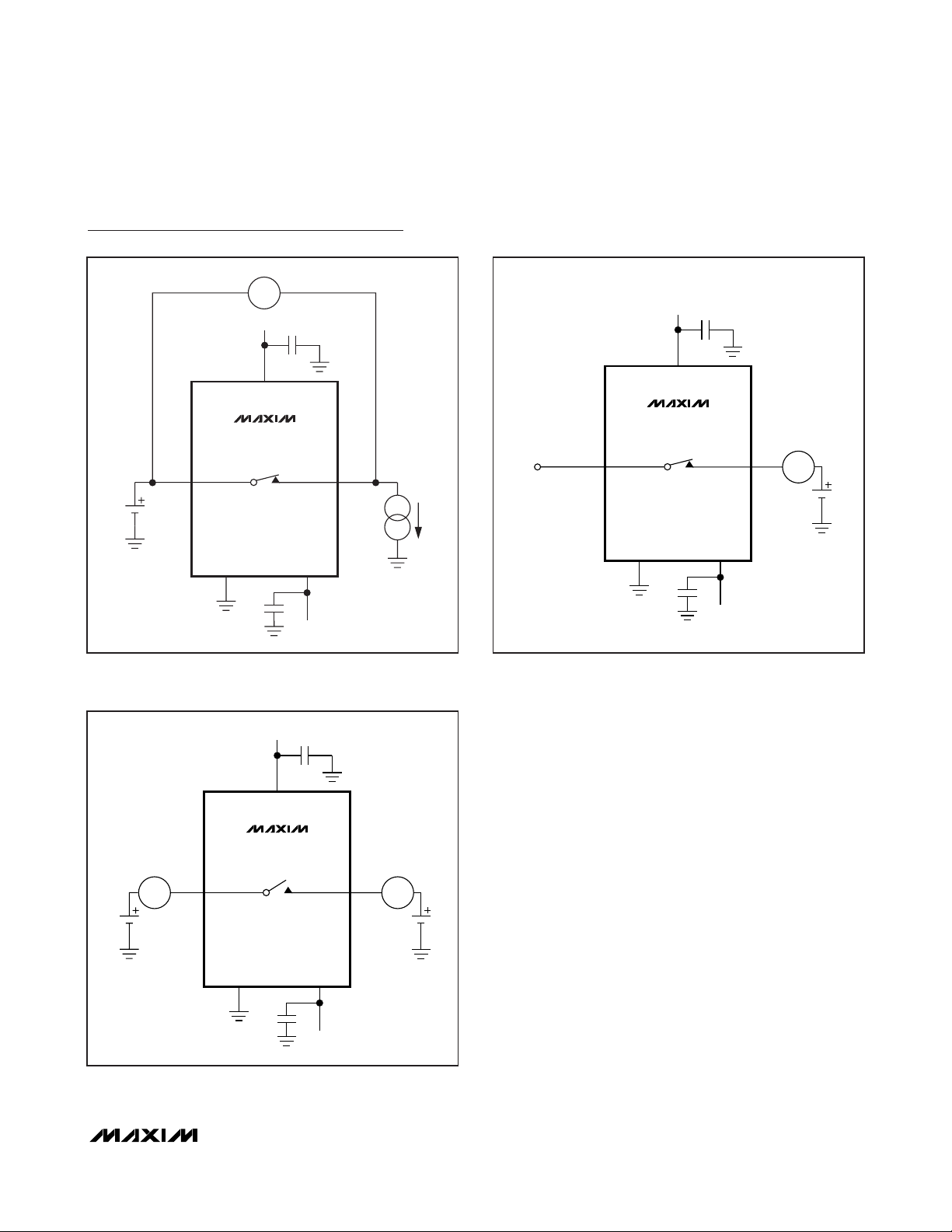
Figure 1. On-Resistance
Figure 2. On-Leakage Current
Figure 3. Off-Leakage Current
V
V
DD
1µF
V
DD
MAX14752
GND
MAX14753
1µF
OUT
OUTA
OUTB
I
IN
V
SS
V
SS
UNCONNECTED
IN_
INA_
INB_
V
IN
IN_
INA_
INB_
GND
V
DD
V
DD
MAX14752
MAX14753
1μF
1μF
I
OUT(ON)
I
OUTA(ON)
OUT
I
OUTB(ON)
OUTA
OUTB
A
V
OUT
V
SS
V
SS
I
IN(OFF)
I
INA(OFF)
I
INB(OFF)
V
IN
IN_
INA_
INB_
GND
V
DD
V
DD
MAX14752
MAX14753
1μF
1μF
I
OUT(OFF)
I
OUTA(OFF)
OUT
I
OUTB(OFF)
OUTA
OUTB
AA
V
OUT
V
SS
V
SS
Page 6

MAX14752/MAX14753
8-Channel/Dual 4-Channel
72V Analog Multiplexers
6 _______________________________________________________________________________________
Test Circuits/Timing Diagrams/Truth Tables (continued)
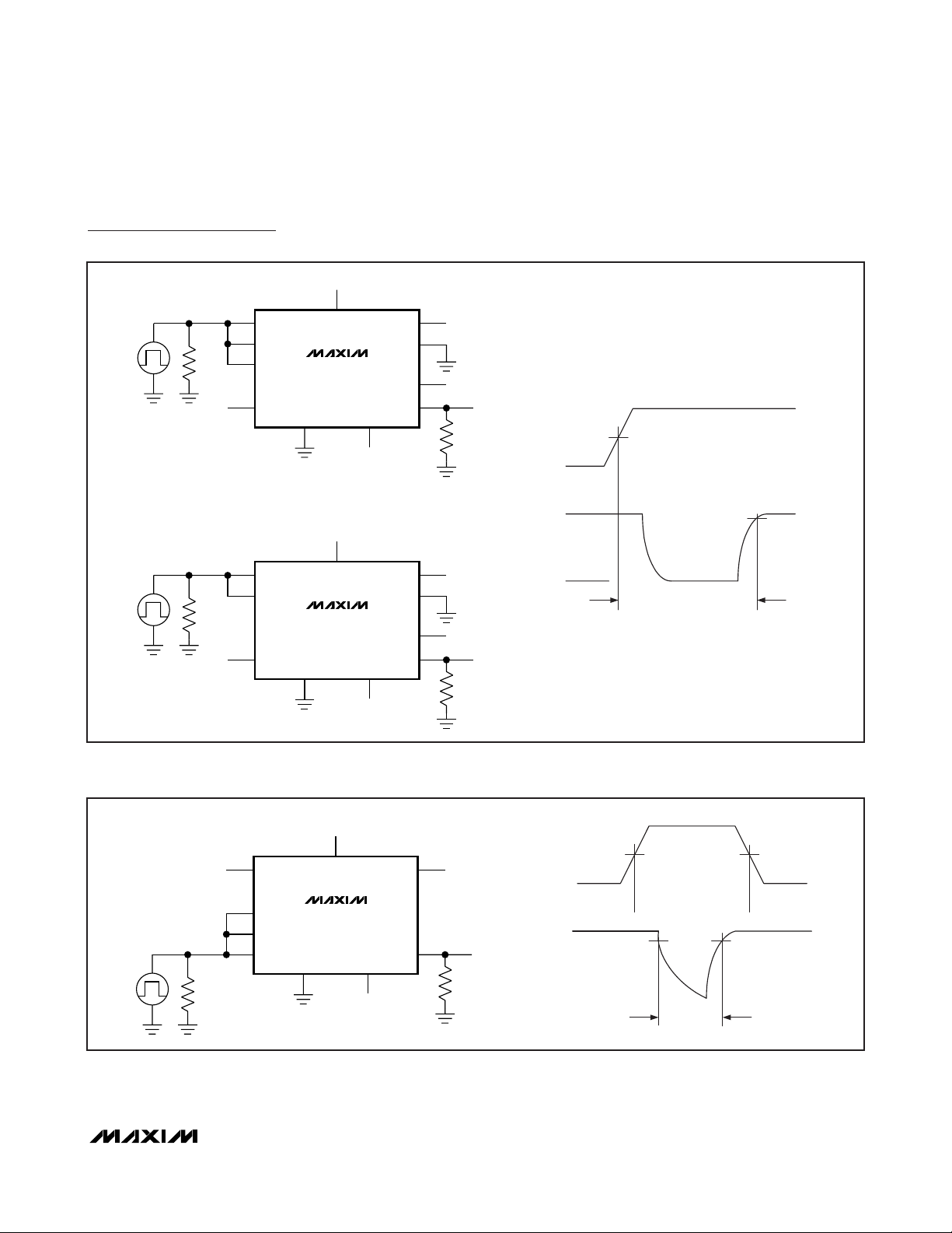
Figure 4. Enable Switching Time
+35V
V
GND
GND
DD
MAX14752
+35V
V
DD
MAX14753
EN
S0
S1
S2
EN
S0
S1
V
SS
-35V
INA1–INA3
INB0–INB3
V
SS
IN0
IN1–IN7
OUT
INA0
OUTA
+10V
10kΩ50Ω
+10V
10kΩ50Ω
V
V
OUT
OUTA
+3.3V
EN
V
OUT
SWITCH
OUTPUT
t
< 20ns
R
< 20ns
t
F
50%
0V
t
ON
, V
OUTA
0V
90%
10%
t
OFF
-35V
Page 7
MAX14752/MAX14753
8-Channel/Dual 4-Channel
72V Analog Multiplexers
_______________________________________________________________________________________ 7
Test Circuits/Timing Diagrams/Truth Tables (continued)
Figure 5. Transition Time
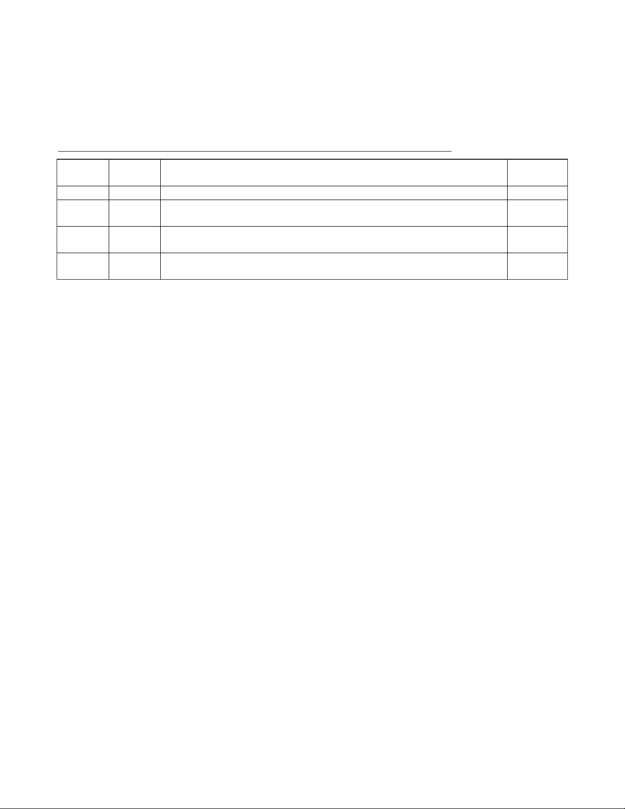
Figure 6. Break-Before-Make Interval
+35V
V
GND
GND
DD
MAX14752
+35V
V
DD
MAX14753
S2
S1
50Ω
+3.3V
50Ω
+3.3V V
S0
EN
S1
S0
EN
V
SS
-35V
INA1–INA2
INB0–INB3
V
SS
-35V
IN1–IN6
OUT
INA0
INA3
OUTA
IN0
IN7
+10V
+10V
10kΩ
+10V
+10V
10kΩ
V
OUT
OUTA
V
OUT
+3.3V
S_
, V
OUTA
SWITCH
OUTPUT
tR < 20ns
< 20ns
t
F
50%
0V
90%
0V
t
TRANS
EN+3.3V
S0
S1
S2
50Ω
GND
+35V
V
DD
MAX14752
V
-35V
SS
IN0–IN7
OUT
+10V
10kΩ
< 20ns
t
R
< 20ns
t
80%
F
t
BBM
+3.3V
S_
0V
V
OUT
V
OUT
SWITCH
OUTPUT
0V
50%
Page 8

MAX14752/MAX14753
8-Channel/Dual 4-Channel
72V Analog Multiplexers
8 _______________________________________________________________________________________
Test Circuits/Timing Diagrams/Truth Tables (continued)
Figure 7. Frequency Response
Figure 8. Off-Isolation
Figure 9. Crosstalk
+35V
1µF
V
DD
+3.3V
EN
MAX14752
IN0
V
IN
NETWORK
ANALYZER
S0
S1
S3
GND
1µF
V
-35V
OUT
SS
+35V
1μF
V
IN
R
= 50Ω
S
IN0
IN7
S0
S1
S2
.
.
.
MAX14752
GND
V
DD
OUT
R
= 1kΩ
L
EN
V
SS
CL = 15pF
ON-LOSS = 20log
V
OUT
V
OUT
MEAS REF
V
OUT
V
IN
R
= 50Ω
S
1μF
+35V
V
IN
IN0
IN1
IN7
S0
S1
S2
.
.
.
MAX14752
GND
V
DD
EN
OUT
V
SS
R
+3.3V
V
= 1kΩ
L
OUT
1μF
OFF ISOLATION = 20log
-35V
V
V
OUT
10nF
IN
CROSSTALK = 20log
-35V
V
V
OUT
IN
Page 9

MAX14752/MAX14753
8-Channel/Dual 4-Channel
72V Analog Multiplexers
_______________________________________________________________________________________ 9
Test Circuits/Timing Diagrams/Truth Tables (continued)
Figure 10. Charge Injection
Table 1. MAX14752 Truth Table
Table 2. MAX14753 Truth Table
+35V
MAX14752
GND
V
DD
OUT
CL = 1nF
V
SS
-35V
IN_
EN
CHANNEL
SELECT
S0
S1
S2
S2 S1 S0 EN OUT
X X X 0 All off
0001IN0
0011IN1
0101IN2
0111IN3
1001IN4
1011IN5
1101IN6
1111IN7
+3.3V
V
EN
0V
V
OUT
V
OUT
0V
ΔV
IS THE MEASURED VOLTAGE DUE TO CHARGE TRANSFER
OUT
ERROR Q WHEN THE CHANNEL TURNS OFF.
Q = CL x ΔV
OUT
S1 S0 EN OUTA OUTB
X X 0 All off All off
0 0 1 INA0 INB0
0 1 1 INA1 INB1
1 0 1 INA2 INB2
1 1 1 INA3 INB3
OFFON ON
ΔV
OUT
Page 10

MAX14752/MAX14753
8-Channel/Dual 4-Channel
72V Analog Multiplexers
10 ______________________________________________________________________________________
Typical Operating Characteristics
(TA= +25°C, unless otherwise noted.)
50
52
56
54
58
60
ON-RESISTANCE
vs. V
OUT
(DUAL SUPPLIES)
MAX14752/3 toc01
R
ON
(Ω)
V
OUT
(V)
-35 5 5 15 25-15-25 35
±35V
±10V
±30V
±20V
20
40
80
60
120
100
140
ON-RESISTANCE vs. V
OUT
AND TEMPERATURE
(DUAL SUPPLIES)
MAX14752/3 toc02
R
ON
(Ω)
V
OUT
(V)
-35 5 5 15 25-15-25 35
VDD = +35V
V
SS
= -35V
TA = +25°C
TA = +85°C
TA = +125°C
TA = -40°C
50
52
56
54
58
60
02010 30 40 50 60 70
ON-RESISTANCE vs. V
OUT
(SINGLE SUPPLY)
MAX14752/3 toc03
V
OUT
(V)
R
ON
(Ω)
+40V+20V
+70V
0
40
80
60
120
100
140
ON-RESISTANCE vs. V
OUT
AND TEMPERATURE
(SINGLE SUPPLY)
MAX14752/3 toc04
R
ON
(Ω)
V
OUT
(V)
-35 50510152025
30-10
-15
-20
-25
-30
35
VDD = +70V
V
SS
= 0V
TA = +25°C
TA = +85°C
TA = +125°C
TA = -40°C
0.01
0.1
1
10
100
-40 -10 5-25 20 35 50 65 80 95 110 125
ON-LEAKAGE vs. TEMPERATURE
MAX14752/3 toc05
TEMPERATURE (°C)
LEAKAGE CURRENT (nA)
VDD = +35V
V
SS
= -35V
I
OUT(ON)
0.01
0.1
1
10
100
-40 -10 5-25 20 35 50 65 80 95 110 125
OFF-LEAKAGE vs. TEMPERATURE
MAX14752/3 toc06
TEMPERATURE (°C)
LEAKAGE CURRENT (nA)
VDD = +35V
V
SS
= -35V
I
OUT(OFF)
I
IN(OFF)
0
100
200
300
400
500
-40 -10 5-25 20 35 50 65 80 95 110 125
CHARGE INJECTION vs. TEMPERATURE
MAX14752/3 toc07
TEMPERATURE (°C)
Q (pC)
VDD = +35V
V
SS
= -35V
250
270
260
300
290
280
310
320
340
330
350
SUPPLY CURRENT vs. TEMPERATURE
MAX14752/3 toc08
I
CC
, I
EE
(μA)
-40 -10 5-25 20 35 50 65 80 95 110 125
TEMPERATURE (°C)
VDD = +35V
V
SS
= -35V
V
EN
= +3.3V
I
CC
I
EE
0
10
30
20
40
50
021345
EN INPUT CURRENT vs. V
S_
MAX14752/3 toc09
VS_ (V)
I
EN
(μA)
VDD = +35V
V
SS
= -35V
Page 11

MAX14752/MAX14753
8-Channel/Dual 4-Channel
72V Analog Multiplexers
______________________________________________________________________________________ 11
Typical Operating Characteristics (continued)
(TA= +25°C, unless otherwise noted.)
0.01 1 100.1 100
CROSSTALK vs. FREQUENCY
MAX14752/3 toc10
FREQUENCY (MHz)
CROSSTALK (dB)
0
-100
-80
-60
-40
-20
VDD = +35V
V
SS
= -35V
0.01 1 100.1 100
OFF-ISOLATION vs. FREQUENCY
MAX14752/3 toc11
FREQUENCY (MHz)
OFF-ISOLATION (dB)
0
-100
-80
-60
-40
-20
VDD = +35V
V
SS
= -35V
0.01 1 100.1 100
ON-LOSS vs. FREQUENCY
MAX14752/3 toc12
FREQUENCY (MHz)
ON-LOSS (dB)
0
-50
-40
-30
-20
-10
VDD = +35V
V
SS
= -35V
0.01 1 100.1 100
TOTAL HARMONIC DISTORTION PLUS NOISE
vs. FREQUENCY
MAX14752/3 toc13
FREQUENCY (MHz)
THD+N (%)
0.005
0
0.001
0.002
0.003
0.004
VDD = +35V
V
SS
= -35V
Page 12

MAX14752/MAX14753
8-Channel/Dual 4-Channel
72V Analog Multiplexers
12 ______________________________________________________________________________________
MAX14752 Pin Description (Single 8-to-1 Mux)
MAX14753 Pin Description (Dual 4-to-1 Mux)
PIN NAME FUNCTION
1 S0 Mux Input Select
2EN
3VSSNegative Supply Voltage. Bypass VSS to GND with a 1µF ceramic capacitor.
4 IN0 Bidirectional Analog Input
5 IN1 Bidirectional Analog Input
6 IN2 Bidirectional Analog Input
7 IN3 Bidirectional Analog Input
8 OUT Bidirectional Analog Output
9 IN7 Bidirectional Analog Input
10 IN6 Bidirectional Analog Input
11 IN5 Bidirectional Analog Input
12 IN4 Bidirectional Analog Input
13 V
14 GND
15 S2 Mux Input Select
16 S1 Mux Input Select
Mux Enable. Drive EN high to enable the device. The EN high voltage defines input logic voltage level for
S0, S1, and S2.
Positive Supply Voltage. Bypass VDD to GND with a 1µF ceramic capacitor.
DD
Ground. Connect GND to V
supply.
for single supply. Bypass GND to VSS with a 1µF ceramic capacitor for dual
SS
PIN NAME FUNCTION
1 S0 Mux Input Select
2EN
3VSSNegative Supply Voltage. Bypass VSS to GND with a 1µF ceramic capacitor.
4 INA0 Bidirectional Analog Input
5 INA1 Bidirectional Analog Input
6 INA2 Bidirectional Analog Input
7 INA3 Bidirectional Analog Input
8 OUTA Bidirectional Analog Output
9 OUTB Bidirectional Analog Output
10 INB3 Bidirectional Analog Input
11 INB2 Bidirectional Analog Input
12 INB1 Bidirectional Analog Input
13 INB0 Bidirectional Analog Input
14 V
15 GND
16 S1 Mux Input Select
Mux Enable. Drive EN high to enable the device. The EN high voltage defines input logic voltage level for
S0 and S1.
Positive Supply Voltage. Bypass VDD to GND with a 1µF ceramic capacitor.
DD
Ground. Connect GND to V
supply.
for single supply. Bypass GND to VSS with a 1µF ceramic capacitor for dual
SS
Page 13

MAX14752/MAX14753
8-Channel/Dual 4-Channel
72V Analog Multiplexers
______________________________________________________________________________________ 13
Detailed Description
The MAX14752/MAX14753 are 8-to-1 and dual 4-to-1
high-voltage analog multiplexers. Both devices feature
60Ω (typ) on-resistance with 0.03Ω (typ) on-resistance
flatness. These low on-resistance multiplexers conduct
equally well in either direction.
The MAX14752 is an 8-to-1 multiplexer and MAX14753
is a dual 4-to-1 multiplexer. Both devices operate with
dual supplies of ±10V to ±36V or a single supply of
+20V to +72V. Both devices can also operate with
unbalanced supplies, such as +36V and -10V. These
multiplexers support rail-to-rail input and output signals.
The control logic level is defined via the EN input. These
devices do not require power-supply sequencing.
Applications Information
Current Through the Mux
The current flowing through each on-channel of the
MAX14752/MAX14753 multiplexers must be limited to
±5mA for normal operation. If the current exceeds this
limit, an internal leakage current from that channel to
VSSappears. Larger input current does not destroy the
device if the max power dissipation is not exceeded.
Input Voltage Clamping
For applications that require input voltages beyond the
normal operating voltages, the internal input diodes to
VDDand VSScan be used to limit the input voltages. As
shown in Figure 11, series resistors can be employed at
the inputs to limit the currents flowing into the diodes during undervoltage and overvoltage conditions. Choose the
limiting resistors such that the input currents are limited to
I
IN_
(max) = 100mA. The values of the current limit resis-
tors can be calculated as the larger of R
LIM+
and R
LIM-.
During an undervoltage or overvoltage condition, the
input impedance is equal to R
LIM
. The additional power
dissipation due to the fault currents needs to be calculated. The MAX14752/MAX14753 multiplexer operates
normally on a channel that is on during an overvoltage
or undervoltage clamping condition on a second channel that is not switched.
Beyond-the-Rail Input
If input voltages are expected to go beyond the supply
voltages, but within the absolute maximum supply voltages of the MAX14752/MAX14753, add two diodes in
series with the supplies as shown in Figure 12.
During undervoltage and overvoltage events, the internal
diodes pull VDD/VSSsupplies up/down. An advantage of
this scheme is that the input impedance is high and
currents do not flow through the MAX14752/MAX14753
during overvoltage and undervoltage events. The input
voltages must be limited to the voltages specified in the
Absolute Maximum Ratings
section.
R
V (max –V
I (max
R
V–V(
LIM+
IN_ DD
IN_
LIM
-
SS IN_
=
=
)
)
mmin
I (max
IN_
)
)
Figure 11. Input Overvoltage and Undervoltage Clamping
R
LIM
R
LIM
R
LIM
R
LIM
R
LIM
R
LIM
R
LIM
R
LIM
V
DD
MAX14752
OUT
CONTROL
V
SS
S0 S2 GNDS1 EN
Page 14

MAX14752/MAX14753
8-Channel/Dual 4-Channel
72V Analog Multiplexers
14 ______________________________________________________________________________________
Figure 12. Beyond-the-Rail Application
1
2
3
4
5
16
15
14
13
12
S1
S2
GND
V
DD
IN0
V
SS
EN
SO
MAX14752
TSSOP
+
TOP VIEW
IN4IN1
6
7
8
11
10
9
IN5
IN6IN3
IN2
IN7 9 OUTBOUT
1
2
3
4
5
16
15
14
13
12
S1
GND
V
DD
INB0INA0
V
SS
EN
SO
INB1INA1
6
7
8
1110INB2
INB3INA3
INA2
OUTA
MAX14753
TSSOP
+
Pin Configurations
Chip Information
PROCESS: CMOS
Package Information
For the latest package outline information and land patterns,
go to www.maxim-ic.com/packages
. Note that a “+”, “#”, or
“-” in the package code indicates RoHS status only. Package
drawings may show a different suffix character, but the drawing
pertains to the package regardless of RoHS status.
PACKAGE
TYPE
PACKAGE
CODE
OUTLINE
NO.
LAND
PATTERN NO.
16 TSSOP U16+1
21-0066 90-0117
V+
V
DD
R
IN_
V
IN
OUT
V
SS
V-
Page 15
MAX14752/MAX14753
8-Channel/Dual 4-Channel
72V Analog Multiplexers
Maxim cannot assume responsibility for use of any circuitry other than circuitry entirely embodied in a Maxim product. No circuit patent licenses are
implied. Maxim reserves the right to change the circuitry and specifications without notice at any time.
Maxim Integrated Products, 120 San Gabriel Drive, Sunnyvale, CA 94086 408-737-7600 ____________________
15
© 2010 Maxim Integrated Products Maxim is a registered trademark of Maxim Integrated Products, Inc.
Revision History
REVISION
NUMBER
0 8/08 Init ial release —
1 10/08
2 2/09 Added capacitance information to EC table
3 7/10
REVISION
DATE
DESCRIPTION
Changed the unit s from mA to μA for V
Characteri stics—Dua l Supplies table
Deleted the “Input Capacitance” parameter from the DC Electrical Characteristics—
Dual Supplies
and VSS supply current in the DC Electrical
DD
PAGES
CHANGED
2
2, 4, 13, 14,
15, 16
3
 Loading...