

Page 1
General Description
The MAX1472 is a crystal-referenced phase-locked
loop (PLL) VHF/UHF transmitter designed to transmit
OOK/ASK data in the 300MHz to 450MHz frequency
range. The MAX1472 supports data rates up to
100kbps, and adjustable output power to more than
+10dBm into a 50Ω load. The crystal-based architecture of the MAX1472 eliminates many of the common
problems with SAW transmitters by providing greater
modulation depth, faster frequency settling, higher
tolerance of the transmit frequency, and reduced
temperature dependence. Combined, these improvements enable better overall receiver performance when
using a superheterodyne receiver such as the MAX1470
or MAX1473.
The MAX1472 is available in a 3mm x 3mm 8-pin
SOT23 package and is specified for the automotive
(-40°C to +125°C) temperature range. An evaluation kit
is available. Contact Maxim Integrated Products for
more information.
Applications
Remote Keyless Entry
RF Remote Controls
Tire Pressure Monitoring
Security Systems
Radio-Controlled Toys
Wireless Game Consoles
Wireless Computer Peripherals
Wireless Sensors
Features
o 2.1V to 3.6V Single-Supply Operation
o Low 5.3mA Operating Supply Current*
o Supports ASK with 90dB Modulation Depth
o Output Power Adjustable to More than +10dBm
o Uses Small Low-Cost Crystal
o Small 3mm
3mm 8-Pin SOT23 Package
o Fast-On Oscillator 220µs Startup Time
MAX1472
300MHz-to-450MHz Low-Power,
Crystal-Based ASK Transmitter
________________________________________________________________
Maxim Integrated Products
1
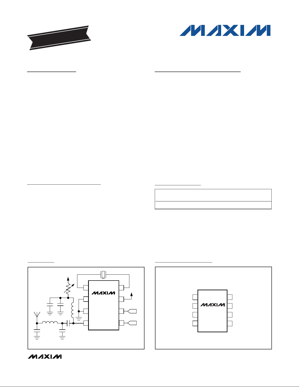
Pin Configuration
Ordering Information
8
7
6
5
1
+
2
3
4
DATA
ENABLE
PAOUT
XTAL2
V
DD
GND
PAGND
XTAL1
MAX1472
3.0V
DATA INPUT
STANDBY OR
POWER-UP
*
680pF220pF
50Ω
ANTENNA
Typical Application Circuit
19-2872; Rev 3; 10/10
For pricing, delivery, and ordering information, please contact Maxim Direct at 1-888-629-4642,
or visit Maxim’s website at www.maxim-ic.com.
EVALUATION KIT
AVAILABLE
*
Optional power adjust resistor.
+
Denotes a lead(Pb)-free/RoHS-compliant package.
T = Tape and reel.
*
At 50% duty cycle (315MHz, 2.7V supply, +10dBm output
power)
PART
MAX1472AKA+T -40°C to +125°C 8 SOT23 AEKS
TEMP
RANGE
PINPACKAGE
TOP
MARK
TOP VIEW
1
XTAL1
2
GND
3
PAGND
4
+
87XTAL2
V
MAX1472
SOT23
DD
DATA
6
ENABLEPAOUT
5
Page 2
MAX1472
300MHz-to-450MHz Low-Power,
Crystal-Based ASK Transmitter
2 _______________________________________________________________________________________
ABSOLUTE MAXIMUM RATINGS
Stresses beyond those listed under “Absolute Maximum Ratings” may cause permanent damage to the device. These are stress ratings only, and functional
operation of the device at these or any other conditions beyond those indicated in the operational sections of the specifications is not implied. Exposure to
absolute maximum rating conditions for extended periods may affect device reliability.
VDDto GND ..........................................................-0.3V to +4.0V
All Other Pins to GND ................................-0.3V to (V
DD
+ 0.3V)
Continuous Power Dissipation (T
A
= +70°C)
8-Pin SOT23 (derate 8.9mW/°C above +70°C)............714mW
Operating Temperature Range .........................-40°C to +125°C
Storage Temperature Range .............................-60°C to +150°C
Lead Temperature (soldering, 10s) .................................+300°C
Soldering Temperature (reflow) .......................................+260°C
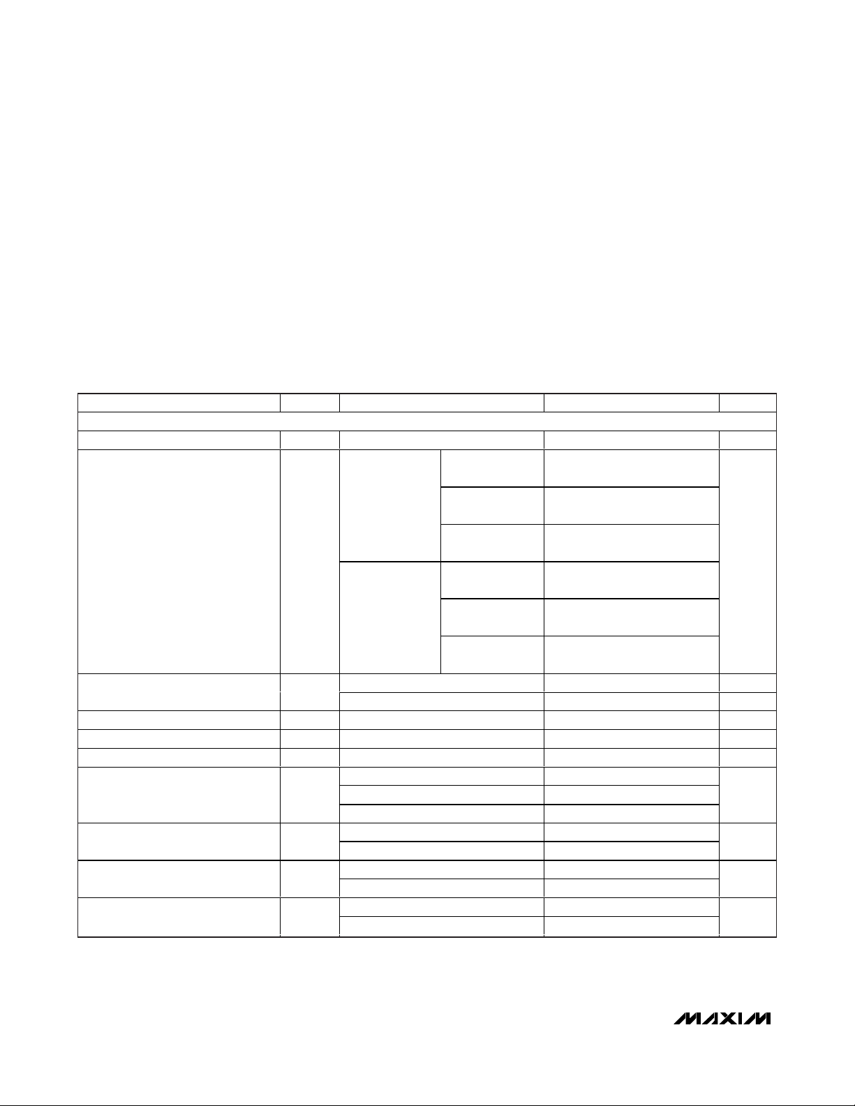
ELECTRICAL CHARACTERISTICS
(
Typical Application Circuit
, output power is referenced to 50Ω, VDD= 2.1V to 3.6V, V
ENABLE
= VDD, TA= -40°C to +125°C, unless
otherwise noted. Typical values are at V
DD
= 2.7V, TA= +25°C, unless otherwise noted.) (Note 1)
PARAMETER SYMBOL CONDITIONS MIN TYP MAX UNITS
SYSTEM PERFORMANCE
Supply Voltage V
Supply Current I
Standby Current I
Frequency Range f
Data Rate (Note 3) 0 100 kbps
Modulation Depth ON to OFF P
Output Power P
Turn-On Time t
Transmit Efficiency with CW
Transmit Efficiency at 50%
Duty Cycle
DD
V
ENABLE
= V
DD
(Note 2)
DD
V
V
V
V
V
ENABLE
= V
DATA
ENABLE
= 0V
DATA
ENABLE
= VDD,
DD
= VDD,
= V
DD
(Note 2)
STDBY
RF
fRF = 433MHz
V
V
V
V
V
V
< VIL, TA < +85°C (Note 3) 5 350 nA
ENABLE
< V
ENABLE
TA < +125°C (Note 3) 1.7 µA
IL
(Note 1) 300 450 MHz
ratio (Note 4) 90 dB
OUT
ENABLE
= V
DATA
ENABLE
= 0V
DATA
= VDD,
DD
= VDD,
TA = +25°C, VDD = 2.7V (Notes 5, 6) 7.3 10.3 12.8
OUT
TA = + 125° C , V
= 2.1V ( N otes 5, 6) 3.3 6.0
D D
TA = -40°C, VDD = 3.6V (Notes 5, 6) 13.7 16.2
ON
To f
To f
f
RF
f
RF
f
RF
f
RF
< 50kHz (Note 7) 220
OFFSET
< 5kHz (Note 7) 450
OFFSET
= 315MHz (Note 8) 43.6
= 433MHz (Note 8) 41.3
= 315MHz (Note 9) 37.6
= 433MHz (Note 9) 35.1
2.1 3.6 V
5.3 9.4
9.1 16.6fRF = 315MHz
1.5 2.3
5.7
9.6
1.7 2.7
mA
dBm
µs
%
%
Page 3
MAX1472
300MHz-to-450MHz Low-Power,
Crystal-Based ASK Transmitter
_______________________________________________________________________________________ 3
ELECTRICAL CHARACTERISTICS (continued)
(
Typical Application Circuit
, output power is referenced to 50Ω, VDD= 2.1V to 3.6V, V
ENABLE
= VDD, TA= -40°C to +125°C, unless
otherwise noted. Typical values are at V
DD
= 2.7V, TA= +25°C, unless otherwise noted.) (Note 1)
Note 1: 100% tested at TA= +25°C. Guaranteed by design and characterization over temperature.
Note 2: 50% duty cycle at 10kHz data.
Note 3: Guaranteed by design and characterization, not production tested.
Note 4: Generally limited by PC board layout.
Note 5: Output power can be adjusted with external resistor.
Note 6: Guaranteed by design and characterization at f
RF
= 315MHz.
Note 7: V
ENABLE
< VILto V
ENABLE
> VIH. f
OFFSET
is defined as the frequency deviation from the desired carrier frequency.
Note 8: V
ENABLE
> VIH, V
DATA
> VIH, Efficiency = P
OUT
/(VDDx IDD).
Note 9: V
ENABLE
> VIH, DATA toggled from VILto VIH, 10kHz, 50% duty cycle, Efficiency = P
OUT
/(VDDx IDD).
PARAMETER SYMBOL CONDITIONS MIN TYP MAX UNITS
PHASE-LOCKED LOOP PERFORMANCE
VCO Gain 330 MHz/V
=100kHz -84
f
OFFSET
f
= 1MHz -91
OFFSET
f
=100kHz -82
OFFSET
= 1MHz -89
f
OFFSET
dBc/Hz
dBc
dBc
Phase Noise
Maximum Carrier Harmonics
Reference Spur
= 315MHz
f
RF
f
= 433MHz
RF
f
= 315MHz -50
RF
= 433MHz -50
f
RF
f
= 315MHz -75
RF
= 433MHz -81
f
RF
Loop Bandwidth 1.6 MHz
Crystal Frequency f
XTAL
/ 32 MHz
f
RF
Oscillator Input Impedance From each XTAL pin to GND 6.2 pF
Frequency Pushing by V
DD
3 ppm/V
DIGITAL INPUTS
Data Input High V
Data Input Low V
IH
IL
V
- 0.25 V
D D
0.25 V
Maximum Input Current 2nA
Pulldown Current 25 µA
Page 4

MAX1472
300MHz-to-450MHz Low-Power,
Crystal-Based ASK Transmitter
4 _______________________________________________________________________________________
Typical Operating Characteristics
(Typical Application Circuit
, VDD= 2.7V, TA= +25°C, unless otherwise noted.)
SUPPLY CURRENT vs. SUPPLY VOLTAGE
MAX1472 toc01
SUPPLY VOLTAGE (V)
SUPPLY CURRENT (mA)
3.22.4 2.8
6
7
8
9
10
11
12
13
5
2.0 3.6
V
ENABLE
= VIH,
V
DATA
= VIH,
f
RF
= 315MHz
-40°C
+25°C
+85°C
+125°C
SUPPLY CURRENT vs. SUPPLY VOLTAGE
MAX1472 toc02
SUPPLY VOLTAGE (V)
SUPPLY CURRENT (mA)
3.22.82.4
1.1
1.2
1.3
1.4
1.5
1.6
1.7
1.8
1.9
2.0 3.6
+85°C
+125°C
-40°C
+25°C
V
ENABLE
= VIH,
V
DATA
= VIL,
f
RF
= 315MHz
SUPPLY CURRENT vs. SUPPLY VOLTAGE
MAX1472 toc03
SUPPLY VOLTAGE (V)
SUPPLY CURRENT (mA)
3.22.82.4
7
8
9
10
11
12
13
6
5
2.0 3.6
V
ENABLE
= VIH,
V
DATA
= VIH,
f
RF
= 433MHz
+25°C
-40°C
+125°C
+85°C
SUPPLY CURRENT vs. SUPPLY VOLTAGE
MAX1472 toc04
SUPPLY VOLTAGE (V)
SUPPLY CURRENT (mA)
3.22.82.4
1.2
1.4
1.6
1.8
2.0
2.2
2.0 3.6
+125°C
-40°C
V
ENABLE
= VIH,
V
DATA
= VIL,
f
RF
= 433MHz
+85°C
+25°C
OUTPUT POWER vs. SUPPLY VOLTAGE
MAX1472 toc05
SUPPLY VOLTAGE (V)
OUTPUT POWER (dBm)
3.22.4 2.8
6
7
8
9
10
11
12
13
14
5
2.0 3.6
V
ENABLE
= VIH,
V
DATA
= VIH,
f
RF
= 315MHz
-40°C
-25°C
+85°C
+125°C
OUTPUT POWER vs. SUPPLY VOLTAGE
MAX1472 toc06
SUPPLY VOLTAGE (V)
OUTPUT POWER (dBm)
3.22.4 2.8
6
7
8
9
10
11
12
13
14
2.0 3.6
V
ENABLE
= VIH,
V
DATA
= VIH,
f
RF
= 433MHz
-40°C
+25°C
+85°C
+125°C
REFERENCE SPUR MAGNITUDE
vs. SUPPLY VOLTAGE
MAX1472 toc07
SUPPLY VOLTAGE (V)
REFERENCE SPUR (dBc)
3.22.82.4
-83
-81
-79
-77
-75
-73
-71
-69
-67
-65
-85
2.0 3.6
315MHz
433MHz
FREQUENCY STABILITY
vs. SUPPLY VOLTAGE
MAX1472 toc08
SUPPLY VOLTAGE (V)
OFFSET FREQUENCY (ppm)
3.22.82.4
-3
-2
-1
0
1
2
-4
2.0 3.6
433MHz
315MHz
TRANSMIT POWER EFFICIENCY
vs. SUPPLY VOLTAGE
MAX1472 toc09
SUPPLY VOLTAGE (V)
EFFICIENCY (%)
3.22.82.4
30
35
40
45
50
55
25
2.0 3.6
+25°C
+85°C
+125°C
-40°C
CW OUTPUT
f
RF
= 315MHz
Page 5

MAX1472
300MHz-to-450MHz Low-Power,
Crystal-Based ASK Transmitter
_______________________________________________________________________________________
5
Typical Operating Characteristics (continued)
(
Typical Application Circuit
, VDD= 2.7V, TA= +25°C, unless otherwise noted.)
TRANSMIT POWER EFFICIENCY
vs. SUPPLY VOLTAGE
50
+25°C
45
40
35
EFFICIENCY (%)
30
25
-40°C
+85°C
2.0 3.6
SUPPLY VOLTAGE (V)
PHASE NOISE vs. OFFSET FREQUENCY
-40
-50
-60
-70
-80
-90
-100
PHASE NOISE (dBc/Hz)
-110
-120
-130
-140
10 10M
f
(Hz)
OFFSET
TRANSMIT POWER EFFICIENCY
vs. SUPPLY VOLTAGE
-40°C
+25°C
+85°C
SUPPLY VOLTAGE (V)
+125°C
OOK OUTPUT AT
50% DUTY CYCLE
= 315MHz
f
RF
3.22.82.4
SUPPLY CURRENT AND OUTPUT POWER
vs. EXTERNAL RESISTOR
POWER
CURRENT
EXTERNAL RESISTOR (Ω)
fRF = 315MHz
100101
+125°C
CW OUTPUT
= 433MHz
f
RF
3.22.82.4
1M100k10k1k100
MAX1472 toc10
EFFICIENCY (%)
MAX1472 toc13
50
45
40
35
30
25
20
2.0 3.6
12
10
8
6
4
OUTPUT POWER (dBm)
2
0
0.1 1000
MAX1472 toc14
45
MAX1472 toc11
12
10
8
6
4
2
0
40
35
30
EFFICIENCY (%)
25
20
10
9
SUPPLY CURRENT (mA)
8
7
6
5
SUPPLY CURRENT (mA)
4
3
2
TRANSMIT POWER EFFICIENCY
vs. SUPPLY VOLTAGE
+25°C
-40°C
+125°C
+85°C
OOK OUTPUT AT
50% DUTY CYCLE
= 433MHz
f
RF
2.0 3.6
SUPPLY VOLTAGE (V)
3.22.4 2.8
SUPPLY CURRENT vs. OUTPUT POWER
fRF = 315MHz
CW
50% DUTY CYCLE
010
OUTPUT POWER (dBm)
862 4
MAX1472 toc12
MAX1472 toc15
25kHz/div
2.5kHz/div
FREQUENCY SETTLING TIME
START: 0s
START: 0s
MAX1472 toc16
1ms
1ms
ENABLE
TRANSITION
FROM LOW
TO HIGH
ENABLE
TRANSITION
FROM LOW
TO HIGH
15%/div
AM DEMODULATION OF PA OUTPUT
START: 0s STOP: 20µs
MAX1472 toc17
DATA RATE
= 100kHz
Page 6

MAX1472
300MHz-to-450MHz Low-Power,
Crystal-Based ASK Transmitter
6 _______________________________________________________________________________________
Detailed Description
The MAX1472 is a highly integrated OOK/ASK transmitter operating over the 300MHz to 450MHz frequency
range. The IC includes a complete PLL and a highly
efficient PA. The device can also be easily placed into
a 5nA low-power shutdown mode.
Shutdown Mode
The ENABLE pin is internally pulled down with a 15µA
current source. If the pin is left unconnected or pulled
low, the MAX1472 goes into shutdown mode, where the
supply current drops to less than 5nA. When ENABLE
is high, the IC is enabled and is ready for transmission
after 220µs (frequency settles to within 50kHz).
The 220µs turn-on time of the MAX1472 is mostly dominated by the crystal oscillator startup time. Once the
oscillator is running, the 1.6MHz PLL loop bandwidth
allows fast-frequency recovery during power-amplifier
toggling.
Phase-Locked Loop
The PLL block contains a phase detector, charge
pump, integrated loop filter, VCO, 32X clock divider,
and crystal oscillator. This PLL requires no external
components, other than a crystal. The relationship
between the carrier and crystal frequency is given by:
f
XTAL
= fRF/ 32
The lock-detect circuit prevents the PA from transmitting until the PLL is locked. In addition, the device shuts
down the PA if the reference frequency is lost.
Power Amplifier (PA)
The PA of the MAX1472 is a high-efficiency, open-drain,
switch-mode amplifier. With proper output matching network, the PA can drive a wide range of impedances,
including the small-loop PC board trace antenna and
any 50Ω antenna. The output-matching network for a
50Ω antenna is shown in the
Typical Application Circuit
.
The output-matching network suppresses the carrier harmonics and transforms the antenna impedance to an
optimal impedance at PAOUT (pin 4), which is about
250Ω .
When the output matching network is properly tuned,
the PA transmits power with high efficiency. The
Typical
Application Circuit
delivers 10.3dBm at 2.7V supply with
9.1mA of supply current. Thus, the overall efficiency is
44%. The efficiency of the PA itself is more than 52%.
Applications Information
Output Power Adjustment
It is possible to adjust the output power down to
-10dBm with the addition of a resistor. The addition of
the power-adjust resistor also reduces power consumption. See the Supply Current and Output Power
vs. External Resistor and Supply Current vs. Output
Power graphs in the
Typical Operating Characteristics
section. It is imperative to add both a low-frequency
and a high-frequency decoupling capacitor as shown
in the
Typical Application Circuit
.
Pin Description
PIN NAME FUNCTION
1 XTAL1 1st Crystal Input. fRF = 32 x f
XTAL
.
2 GND Ground. Connect to system ground.
3 PAGND Ground for the Power Amplifier (PA). Connect to system ground.
4 PAOUT
Power-Amplifier Output. This output requires a pullup inductor to the supply voltage, which may be part
of the output-matching network to a 50Ω antenna.
5
Standby/Power-Up Input. A logic low on ENABLE places the device in standby mode.
6 DATA OOK Data Input. Power amplifier is ON when DATA is high.
7VDDSupply Voltage. Bypass to GND with capacitor as close to the pin as possible.
8 XTAL2 2nd Crystal Input. fRF = 32 x f
XTAL
.
ENABLE
Page 7

MAX1472
300MHz-to-450MHz Low-Power,
Crystal-Based ASK Transmitter
_______________________________________________________________________________________ 7
Crystal Oscillator
The crystal oscillator in the MAX1472 is designed to
present a capacitance of approximately 3.1pF between
the XTAL1 and XTAL2 pins. If a crystal designed to
oscillate with a different load capacitance is used, the
crystal is pulled away from its intended operating frequency, thus introducing an error in the reference frequency. Crystals designed to operate with higher
differential load capacitance always pull the reference
frequency higher. For example, a 9.84375MHz crystal
designed to operate with a 10pF load capacitance
oscillates at 9.84688MHz with the MAX1472, causing
the transmitter to be transmitting at 315.1MHz rather
than 315.0MHz, an error of about 100kHz, or 320ppm.
In actuality, the oscillator pulls every crystal. The crystal’s natural frequency is really below its specified frequency, but when loaded with the specified load
capacitance, the crystal is pulled and oscillates at its
specified frequency. This pulling is already accounted
for in the specification of the load capacitance.
Additional pulling can be calculated if the electrical
parameters of the crystal are known. The frequency
pulling is given by:
where:
f
p
is the amount the crystal frequency is pulled in ppm.
Cmis the motional capacitance of the crystal.
C
case
is the case capacitance.
C
spec
is the specified load capacitance.
C
load
is the actual load capacitance.
When the crystal is loaded as specified, i.e., C
load
=
C
spec
, the frequency pulling equals zero.
Output Matching to 50
ΩΩ
When matched to a 50Ω system, the MAX1472 PA is
capable of delivering more than +10dBm of output
power at VDD= 2.7V. The output of the PA is an opendrain transistor that requires external impedance
matching and pullup inductance for proper biasing.
The pullup inductance from PA to VDDserves three
main purposes: It resonates the capacitance of the PA
output, provides biasing for the PA, and becomes a
high-frequency choke to reduce the RF energy coupling into V
DD
. The recommended output-matching net-
work topology is shown in the
Typical Application
Circuit
. The matching network transforms the 50Ω load
to a higher impedance at the output of the PA in addition to forming a bandpass filter that provides attenuation for the higher order harmonics.
Output Matching to PC Board Loop
Antenna
In most applications, the MAX1472 PA output has to be
impedance matched to a small-loop antenna. The
antenna is usually fabricated out of a copper trace on a
PC board in a rectangular, circular, or square pattern.
The antenna has an impedance that consists of a lossy
component and a radiative component. To achieve
high radiating efficiency, the radiative component
should be as high as possible, while minimizing the
lossy component. In addition, the loop antenna has an
inherent loop inductance associated with it (assuming
the antenna is terminated to ground). For example, in a
typical application, the radiative impedance is less than
0.5Ω, the lossy impedance is less than 0.7Ω, and the
inductance is approximately 50nH to 100nH.
The objective of the matching network is to match the
PA output to the small loop antenna. The matching
components thus transform the low radiative and resistive parts of the antenna into the much higher value of
the PA output, which gives higher efficiency. The low
radiative and lossy components of the small loop antenna result in a higher Q matching network than the 50Ω
network; thus, the harmonics are lower.
f
C
CCCC
p
m
case load case spec
=
+
−
+
⎛
⎝
⎜
⎞
⎠
⎟
×
2
11
10
6
Page 8

MAX1472
Layout Considerations
A properly designed PC board is an essential part of
any RF/microwave circuit. On the PA output, use controlled-impedance lines and keep them as short as
possible to minimize losses and radiation. At high frequencies, trace lengths that are on the order of λ/10 or
longer can act as antennas.
Keeping the traces short also reduces parasitic inductance. Generally, 1in of PC board trace adds about
20nH of parasitic inductance. The parasitic inductance
can have a dramatic effect on the effective inductance.
For example, a 0.5in trace connecting a 100nH inductor adds an extra 10nH of inductance, or 10%.
To reduce the parasitic inductance, use wider traces
and a solid ground or power plane below the signal
traces. Using a solid ground plane can reduce the parasitic inductance from approximately 20nH/in to 7nH/in.
Also, use low-inductance connections to ground on all
GND pins, and place decoupling capacitors close to all
V
DD
connections.
300MHz-to-450MHz Low-Power,
Crystal-Based ASK Transmitter
8 _______________________________________________________________________________________
Functional Diagram
Chip Information
PROCESS: CMOS
Package Information
For the latest package outline information and land patterns,
go to www.maxim-ic.com/packages
. Note that a “+”, “#”, or
“-” in the package code indicates RoHS status only. Package
drawings may show a different suffix character, but the drawing
pertains to the package regardless of RoHS status.
PACKAGE
TYPE
PACKAGE
CODE
OUTLINE NO.
LAND
PATTERN NO.
8 SOT23 K8SN+1
21-0078
90-0176
DATA
ENABLE
XTAL1
XTAL2
LOCK DETECT
MAX1472
OSCILLATOR
AND
GATE
32 x PLL
CRYSTAL-
DRIVER
V
DD
PA
PAOUT
PAGND
GND
Page 9

MAX1472
300MHz-to-450MHz Low-Power,
Crystal-Based ASK Transmitter
Maxim cannot assume responsibility for use of any circuitry other than circuitry entirely embodied in a Maxim product. No circuit patent licenses are
implied. Maxim reserves the right to change the circuitry and specifications without notice at any time.
Maxim Integrated Products, 120 San Gabriel Drive, Sunnyvale, CA 94086 408-737-7600 _____________________
9
© 2010 Maxim Integrated Products Maxim is a registered trademark of Maxim Integrated Products, Inc.
Revision History
REVISION
NUMBER
1 4/05 — —
2 6/09
3 10/10
REVISION
DATE
DESCRIPTION
Updated EC table Ma x supply currents, added lead-free note, and corrected
Electrical Characteristics notes
Removed Maximum Crystal Inductance spec from Electrical Characteristics
table
PAGES
CHANGED
1, 2, 3, 6, 8
3
 Loading...