

Page 1
General Description
The MAX1471 low-power, CMOS, superheterodyne, RF
dual-channel receiver is designed to receive both amplitude-shift-keyed (ASK) and frequency-shift-keyed (FSK)
data without reconfiguring the device or introducing any
time delay normally associated with changing modulation schemes. The MAX1471 requires few external components to realize a complete wireless RF digital data
receiver for the 300MHz to 450MHz ISM bands.
The MAX1471 includes all the active components
required in a superheterodyne receiver including: a lownoise amplifier (LNA), an image-reject (IR) mixer, a fully
integrated phase-locked loop (PLL), local oscillator
(LO), 10.7MHz IF limiting amplifier with received-signalstrength indicator (RSSI), low-noise FM demodulator,
and a 3V voltage regulator. Differential peak-detecting
data demodulators are included for both the FSK and
ASK analog baseband data recovery. The MAX1471
includes a discontinuous receive (DRX) mode for lowpower operation, which is configured through a serial
interface bus.
The MAX1471 is available in a 32-pin thin QFN package
and is specified over the automotive -40°C to +125°C
temperature range.
Applications
Automotive Remote Keyless Entry (RKE)
Tire Pressure Monitoring Systems
Garage Door Openers
Wireless Sensors
Wireless Keys
Security Systems
Medical Systems
Home Automation
Local Telemetry Systems
Features
o ASK and FSK Demodulated Data on Separate
Outputs
o Specified over Automotive -40°C to +125°C
Temperature Range
o Low Operating Supply Voltage Down to 2.4V
o On-Chip 3V Regulator for 5V Operation
o Low Operating Supply Current
7mA Continuous Receive Mode
1.1µA Deep-Sleep Mode
o Discontinuous Receive (DRX) Low-Power
Management
o Fast-On Startup Feature < 250µs
o Integrated PLL, VCO, and Loop Filter
o 45dB Integrated Image Rejection
o RF Input Sensitivity*
ASK: -114dBm
FSK: -108dBm
o Selectable IF BW with External Filter
o Programmable Through Serial User Interface
o RSSI Output and High Dynamic Range with AGC
MAX1471
315MHz/434MHz Low-Power, 3V/5V
ASK/FSK Superheterodyne Receiver
________________________________________________________________
Maxim Integrated Products
1
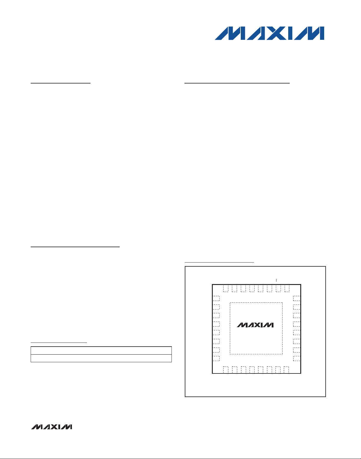
Pin Configuration
19-3272; Rev 4; 9/11
For pricing, delivery, and ordering information, please contact Maxim Direct at 1-888-629-4642,
or visit Maxim’s website at www.maxim-ic.com.
*
0.2% BER, 4kbps, Manchester-encoded data, 280kHz IF BW
Ordering Information
+
Denotes a lead(Pb)-free/RoHS-compliant package.
/V denotes an automotive qualified part.
**
EP = Exposed pad.
PART TEMP RANGE PIN-PACKAGE
MAX1471ATJ/V+ -40°C to +125°C 32 Thin QFN-EP**
TOP VIEW
HVIN
MIXIN-
SCLK
MIXOUT
DIO
AGND
CS
IFIN-
FDATA
25
DVDD
24
23
DGND
22
DFF
21
OPF+
20
DSF+
19
DSF-
PDMAXF
18
17
PDMINF
16
IFIN+
DSA-
DSA+
OPA+
DFA
XTAL2
XTAL1
AVDD
LNAIN
ADATA
PDMINA
PDMAXA
32+31 30 29 28 27 26
1
2
3
4
LNAOUT
MAX1471
MIXIN+
THIN QFN
5
6
7
8
9 101112131415
LNASRC
Page 2
MAX1471
315MHz/434MHz Low-Power, 3V/5V
ASK/FSK Superheterodyne Receiver
2 _______________________________________________________________________________________
ABSOLUTE MAXIMUM RATINGS
Stresses beyond those listed under “Absolute Maximum Ratings” may cause permanent damage to the device. These are stress ratings only, and functional
operation of the device at these or any other conditions beyond those indicated in the operational sections of the specifications is not implied. Exposure to
absolute maximum rating conditions for extended periods may affect device reliability.
High-Voltage Supply, HVIN to DGND ......................-0.3V, +6.0V
Low-Voltage Supply, AVDD and DVDD to AGND ....-0.3V, +4.0V
SCLK, DIO, CS, ADATA,
FDATA ...................................(DGND - 0.3V) to (HVIN + 0.3V)
All Other Pins............................(AGND - 0.3V) to (AVDD + 0.3V)
Continuous Power Dissipation (T
A
= +70°C)
32-Pin Thin QFN (derate 21.3mW/°C above +70°C) ...1702mW
Operating Temperature Range .........................-40°C to +125°C
Junction Temperature......................................................+150°C
Storage Temperature Range .............................-65°C to +150°C
Lead Temperature (soldering, 10s) ................................ +300°C
Soldering Temperature (reflow) ...................................... +260°C
DC ELECTRICAL CHARACTERISTICS
(
Typical Application Circuit
, V
AVDD
= V
DVDD
= V
HVIN
= +2.4V to +3.6V, fRF= 300MHz to 450MHz, TA= -40°C to +125°C, unless other-
wise noted. Typical values are at V
AVDD
= V
DVDD
= V
HVIN
= +3.0V, fRF= 434 MHz, TA= +25°C, unless otherwise noted.) (Note 1)
PARAMETER SYMBOL CONDITIONS MIN TYP MAX UNITS
GENERAL CHARACTERISTICS
Supply Voltage (5V) HVIN
Supply Voltage (3V) V
Supply Current I
Startup Time t
DIGITAL OUTPUTS (DIO, ADATA, FDATA)
Output High Voltage V
Output Low Voltage V
DIGITAL INPUTS (CS, DIO, SCLK)
Input High Threshold V
Input Low Threshold V
DD
ON
DD
OH
OL
IH
IL
AVDD and DVDD unconnected from HVIN,
but connected together
HVIN, AVDD, and DVDD connected to
power supply
TA < +85°C
TA < +105°C
(Note 2)
TA < +125°C
(Note 2)
Time for final signal detection, does not
include baseband filter settling (Note 2)
I
I
= 250µA (Note 2)
SOURCE
= 250µA (Note 2) 0.15 V
SINK
4.5 5.0 5.5 V
2.4 3.0 3.6 V
Operating 7.0 8.4 mA
Polling duty cycle: 10%
duty cycle
DRX mode OFF current 5.0 14.2
Deep-sleep current 1.1 7.1
Operating 8.5 mA
Polling duty cycle: 10%
duty cycle
DRX mode OFF current 15.5
Deep-sleep current 13.4
Operating 8.6 mA
Polling duty cycle: 10%
duty cycle
DRX mode OFF current 44.1
Deep-sleep current 36.4
0.9 x
V
HVIN
705 855
200 250 µs
V
-
HVIN
0.15
.
865
900
0.1 x
V
HVIN
µA
µA
µA
V
V
V
Page 3
MAX1471
315MHz/434MHz Low-Power, 3V/5V
ASK/FSK Superheterodyne Receiver
_______________________________________________________________________________________ 3
DC ELECTRICAL CHARACTERISTICS (continued)
(
Typical Application Circuit
, V
AVDD
= V
DVDD
= V
HVIN
= +2.4V to +3.6V, fRF= 300MHz to 450MHz, TA= -40°C to +125°C, unless other-
wise noted. Typical values are at V
AVDD
= V
DVDD
= V
HVIN
= +3.0V, fRF= 434 MHz, TA= +25°C, unless otherwise noted.) (Note 1)
AC ELECTRICAL CHARACTERISTICS
(
Typical Application Circuit
, V
AVDD
= V
DVDD
= V
HVIN
= +2.4V to +3.6V, fRF= 300MHz to 450MHz, TA= -40°C to +125°C, unless other-
wise noted. Typical values are at V
AVDD
= V
DVDD
= V
HVIN
= +3.0V, fRF= 434 MHz, TA= +25°C, unless otherwise noted.) (Note 1)
PARAMETER
CONDITIONS
UNITS
GENERAL CHARACTERISTICS
ASK
Receiver Sensitivity RF
IN
0.2% BER, 4kbps
Manchester Code, 280kHz
IF BW, 50Ω
FSK
dBm
Maximum Receiver Input Power
Level
RF
MAX
0
dBm
Receiver Input Frequency Range
f
RF
450
MHz
Receiver Image Rejection IR (Note 3) 45 dB
LNA/MIXER (Note 4)
LNA Input Impedance
Normalized to 50Ω
Voltage Conversion Gain (HighGain Mode)
dB
Input-Referred 3rd-Order
Intercept Point (High-Gain Mode)
-38
dBm
Voltage Conversion Gain (LowGain Mode)
dB
Input-Referred 3rd-Order
Intercept Point (Low-Gain Mode)
-5
dBm
LO Signal Feedthrough to
Antenna
-90
dBm
Mixer Output Impedance
Ω
IF
Input Impedance Z
IN_IF
Ω
Operating Frequency f
IF
MHz
3dB Bandwidth 10
MHz
FM DEMODULATOR
Demodulator Gain G
FM
2.2
mV/kHz
PARAMETER SYMBOL CONDITIONS MIN TYP MAX UNITS
Input-High Leakage Current I
Input-Low Leakage Current I
Input Capacitance C
VOLTAGE REGULATOR
Output Voltage V
REG
IH
IL
IN
(Note 2) -20 µA
(Note 2) 20 µA
(Note 2) 2.0 pF
V
HVIN
= 5.0V, I
= 7.0mA 3.0 V
LOAD
SYMBOL
Z
IN_LNA
MIN TYP MAX
-114
-108
300
fRF = 315MHz 1 - j4.7
fRF = 434MHz 1 - j3.4
47.5
12.2
Z
OUT_MIX
330
330
10.7
Page 4
MAX1471
315MHz/434MHz Low-Power, 3V/5V
ASK/FSK Superheterodyne Receiver
4 _______________________________________________________________________________________
AC ELECTRICAL CHARACTERISTICS (continued)
(
Typical Application Circuit
, V
AVDD
= V
DVDD
= V
HVIN
= +2.4V to +3.6V, fRF= 300MHz to 450MHz, TA= -40°C to +125°C, unless other-
wise noted. Typical values are at V
AVDD
= V
DVDD
= V
HVIN
= +3.0V, fRF= 434 MHz, TA= +25°C, unless otherwise noted.) (Note 1)
Note 1: Production tested at TA= +85°C. Guaranteed by design and characterization over entire temperature range.
Note 2: Guaranteed by design and characterization. Not production tested.
Note 3: The oscillator register (0x3) is set to the nearest integer result of f
XTAL
/ 100kHz (see the
Oscillator Frequency Register
section).
Note 4: Input impedance is measured at the LNAIN pin. Note that the impedance at 315MHz includes the 15nH inductive degeneration
from the LNA source to ground. The impedance at 434MHz includes a 10nH inductive degeneration connected from the LNA
source to ground. The equivalent input circuit is 50Ω in series with 2.2pF. The voltage conversion gain is measured with the
LNA input matching inductor, the degeneration inductor, and the LNA/mixer resonator in place, and does not include the IF filter insertion loss.
PARAMETER SYMBOL CONDITIONS MIN TYP MAX UNITS
ANALOG BASEBAND
Maximum Data Filter Bandwidth BW
Maximum Data Slicer Bandwidth BW
Maximum Peak Detector
Bandwidth
Maximum Data Rate
CRYSTAL OSCILLATOR
Crystal Frequency f
Frequency Pulling by V
Crystal Load Capacitance 3pF
DIGITAL INTERFACE TIMING (see Figure 8)
Minimum SCLK Setup to Falling
Edge of CS
Minimum CS Falling Edge to
SCLK Rising-Edge Setup Time
Minimum CS Idle Time t
Minimum CS Period t
Maximum SCLK Falling Edge to
Data Valid Delay
Minimum Data Valid to SCLK
Rising-Edge Setup Time
Minimum Data Valid to SCLK
Rising-Edge Hold Time
Minimum SCLK High Pulse Width t
Minimum SCLK Low Pulse Width t
Minimum CS Rising Edge to
SCLK Rising-Edge Hold Time
Maximum CS Falling Edge to
Output Enable Time
Maximum CS Rising Edge to
Output Disable Time
DD
BW
XTAL
t
SC
t
CSS
CSI
CS
t
DO
t
DS
t
DH
CH
CL
t
CSH
t
DV
t
TR
DF
DS
PD
Manchester coded 33
Nonreturn to zero (NRZ) 66
50 kHz
100 kHz
50 kHz
kbps
9.04 13.728 MHz
3 ppm/V
30 ns
30 ns
125 ns
2.125 µs
80 ns
30 ns
30 ns
100 ns
100 ns
30 ns
25 ns
25 ns
Page 5
MAX1471
315MHz/434MHz Low-Power, 3V/5V
ASK/FSK Superheterodyne Receiver
_______________________________________________________________________________________
5
1
)
)
0
)
)
MAX1471 t 06
(°C)
0
0
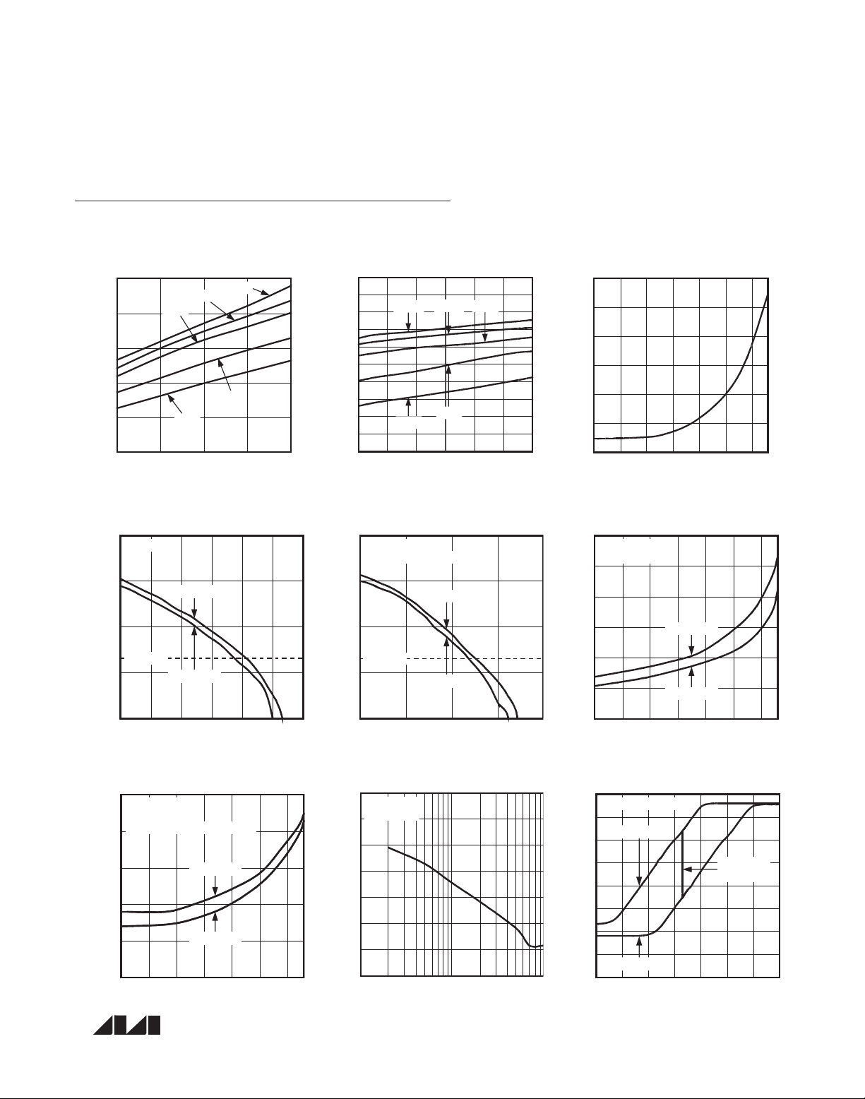
Typical Operating Characteristics
(
Typical Application Circuit
, V
AVDD
= V
DVDD
= V
HVIN
= +3.0V, fRF= 434MHz, TA= +25°C, unless otherwise noted.)
SUPPLY CURRENT
vs. SUPPLY VOLTAGE
8.0
+105°C
7.6
7.2
6.8
SUPPLY CURRENT (mA)
6.4
6.0
2.4 2.7 3.0 3.3 3.6
+85°C
-40°C
SUPPLY VOLTAGE (V)
BIT-ERROR RATE
vs. AVERAGE INPUT POWER (ASK DATA
100
280kHz IF BW
10
fRF = 434MHz
+125°C
+25°C
MAX1471 toc01
SUPPLY CURRENT
vs. RF FREQUENCY
8.0
7.8
7.6
7.4
7.2
7.0
6.8
6.6
SUPPLY CURRENT (mA)
6.4
6.2
6.0
300 325 375350 400 425 450
+105°C
+125°C
+25°C
-40°C
RF FREQUENCY (MHz)
BIT-ERROR RATE
vs. AVERAGE INPUT POWER (FSK DATA
100
280kHz IF BW
FREQUENCY DEVIATION = ±50kHz
10
fRF = 434MHz
DEEP-SLEEP CURRENT
vs. TEMPERATURE
TEMPERATURE (°C)
SENSITIVITY
vs. TEMPERATURE (ASK DATA)
280kHz IF BW
0.2% BER
+85°C
MAX1471 toc02
12
10
8
6
4
DEEP-SLEEP CURRENT (µA)
2
0
-40 10-15 35 60 85 110
-102
-105
-108
MAX1471 toc03
1
0.2% BER
BIT-ERROR RATE (%)
0.1
0.01
-123 -121 -119 -117 -115 -113
fRF = 315MHz
AVERAGE INPUT POWER (dBm
SENSITIVITY
vs. TEMPERATURE (FSK DATA)
-102
280kHz IF BW
0.2% BER
FREQUENCY DEVIATION = ±50kHz
-104
-106
-108
SENSITIVITY (dBm)
-110
-112
-40 10-15 35 60 85 110
fRF = 434MHz
fRF = 315MHz
-1
1
BIT-ERROR RATE
0.2% BER
0.1
0.01
-115 -110-113 -108 -1
fRF = 315MHz
AVERAGE INPUT POWER (dBm
SENSITIVITY vs. FREQUENCY
DEVIATION (FSK DATA)
-98
280kHz IF BW
0.2% BER
-100
-102
-104
-106
SENSITIVITY (dBm)
-108
-110
-112
1101
-111
-114
SENSITIVITY (dBm)
-117
-120
-40 10-15 35 60 85 110
fRF = 434MHz
fRF = 315MHz
TEMPERATURE
RSSI vs. RF INPUT POWER
1.6
AGC HYSTERESIS: 3dB
1.4
HIGH-GAIN MODE
1.2
1.0
0.8
RSSI (V)
0.6
0.4
0.2
LOW-GAIN MODE
0
-130 -90 -70-110
-50
AGC SWITCH
POINT
-30 -10 1
Page 6
MAX1471
315MHz/434MHz Low-Power, 3V/5V
ASK/FSK Superheterodyne Receiver
6 _______________________________________________________________________________________
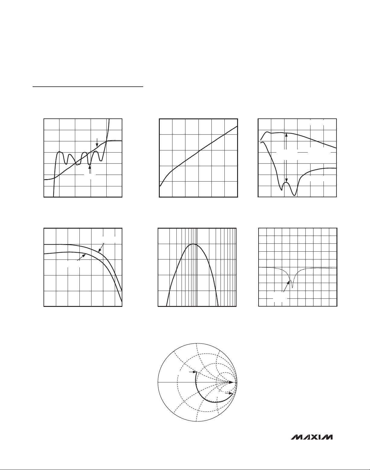
B
Typical Operating Characteristics (continued)
(
Typical Application Circuit
, V
AVDD
= V
DVDD
= V
HVIN
= +3.0V, fRF= 434MHz, TA= +25°C, unless otherwise noted.)
RSSI AND DELTA vs. IF INPUT POWER
2.1
1.8
1.5
1.2
RSSI (V)
0.9
0.6
0.3
0
-90 -50-70 -30 -10 10
RF INPUT POWER (dBm)
IMAGE REJECTION
vs. TEMPERATURE
48
46
44
42
IMAGE REJECTION (dB)
40
38
-40 10-15 35 60 85 110
fRF = 434MHz
DELTA
MAX1471 toc10
RSSI
fRF = 315MHz
°
3.5
2.5
1.5
0.5
-0.5
-1.5
-2.5
-3.5
MAX1471 toc13
FSK DEMODULATOR OUTPUT
vs. IF FREQUENCY
2.0
1.6
1.2
DELTA (%)
0.8
0.4
FSK DEMODULATOR OUTPUT (V)
0
10.4 10.5 10.710.6 10.8 10.9 11.0
IF FREQUENCY (MHz)
NORMALIZED IF GAIN
vs. IF FREQUENCY
5
0
-5
-10
NORMALIZED IF GAIN (dBm)
-15
-20
1 10 100
IF FREQUENCY (MHz)
SYSTEM VOLTAGE GAIN
vs. IF FREQUENCY
60
50
MAX1471 toc11
40
30
20
SYSTEM GAIN (dB)
10
0
-10
010155 202530
45dB IMAGE
REJECTION
IF FREQUENCY (MHz)
UPPER SIDEBAND
LOWER SIDEBAND
S11 LOG-MAGNITUDE PLOT WITH
MATCHING NETWORK OF RFIN (434MHz)
10dB/
MAX1471 toc14
div
0dB
434MHz
-16.4dB
START: 50MHz STOP: 1GHz
FROM RFIN
TO MIXOUT
= 434MHz
f
RF
MAX1471 toc12
MAX1471 toc15
0d
S11 SMITH CHART OF RFIN (434MHz)
500MHz
MAX1471 toc16
200MHz
Page 7
MAX1471
315MHz/434MHz Low-Power, 3V/5V
ASK/FSK Superheterodyne Receiver
_______________________________________________________________________________________
7
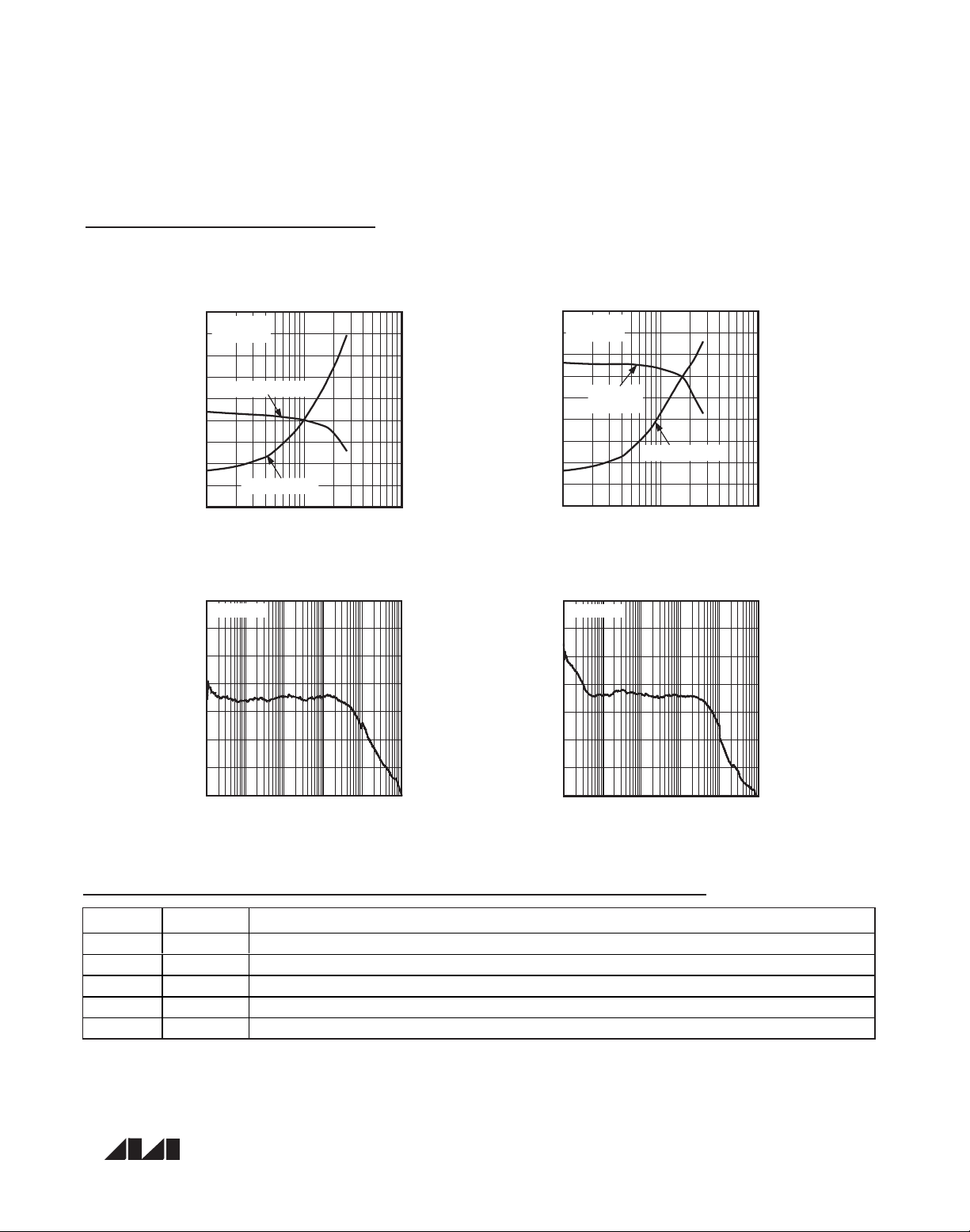
Typical Operating Characteristics (continued)
(
Typical Application Circuit
, V
AVDD
= V
DVDD
= V
HVIN
= +3.0V, fRF= 434MHz, TA= +25°C, unless otherwise noted.)
Pin Description
INPUT IMPEDANCE vs. INDUCTIVE
DEGENERATION
90
fRF = 315MHz
80
L1 = 0nH
70
60
IMAGINARY IMPEDANCE
50
40
30
REAL IMPEDANCE (Ω)
20
10
0
REAL IMPEDANCE
1 100
INDUCTIVE DEGENERATION (nH)
10
PHASE NOISE vs. OFFSET FREQUENCY
-50
fRF = 315MHz
-60
-70
-80
-90
PHASE NOISE (dBc/Hz)
-100
MAX1471 toc17
-125
-150
-175
-200
-225
-250
-275
-300
-325
-350
MAX1471 toc19
INPUT IMPEDANCE vs. INDUCTIVE
90
DEGENERATION
fRF = 434MHz
80
L1 = 0nH
70
60
50
40
30
IMAGINARY IMPEDANCE (Ω)
REAL IMPEDANCE (Ω)
20
10
IMAGINARY
IMPEDANCE
REAL IMPEDANCE
0
1 100
INDUCTIVE DEGENERATION (nH)
10
MAX1471 toc18
-125
-150
-175
-200
-225
-250
-275
-300
-325
-350
IMAGINARY IMPEDANCE (Ω)
PHASE NOISE vs. OFFSET FREQUENCY
-50
fRF = 434MHz
-60
-70
-80
-90
PHASE NOISE (dBc/Hz)
-100
MAX1471 toc20
-110
-120
100 1k 1M 10M
10k 100k
OFFSET FREQUENCY (Hz)
-110
-120
100 1k 1M 10M
10k 100k
OFFSET FREQUENCY (Hz)
PIN NAME FUNCTION
1 DSA- Inverting Data Slicer Input for ASK Data
2 DSA+ Noninverting Data Slicer Input for ASK Data
3 OPA+ Noninverting Op-Amp Input for the ASK Sallen-Key Data Filter
4 DFA Data-Filter Feedback Node. Input for the feedback of the ASK Sallen-Key data filter.
5 XTAL2 2nd Crystal Input
Page 8
MAX1471
315MHz/434MHz Low-Power, 3V/5V
ASK/FSK Superheterodyne Receiver
8 _______________________________________________________________________________________
Pin Description (continued)
PIN NAME FUNCTION
6 XTAL1 1st Crystal Input
7 AVDD
8 LNAIN Low-Noise Amplifier Input
9 LNASRC
10 LNAOUT Low-Noise Amplifier Output. Connect to mixer through an LC tank filter.
11 MIXIN+ Differential Mixer Input. Must be AC-coupled to driving input.
12 MIXIN- Differential Mixer Input. Bypass to AGND with a capacitor.
13 MIXOUT 330Ω Mixer Output. Connect to the input of the 10.7MHz IF filter.
14 AGND Analog Ground
15 IFIN- Differential 330Ω IF Limiter Amplifier Input. Bypass to AGND with a capacitor.
16 IFIN+ Differential 330Ω IF Limiter Amplifier Input. Connect to output of the 10.7MHz IF filter.
17 PDMINF
18 PDMAXF
19 DSF- Inverting Data Slicer Input for FSK Data
20 DSF+ Noninverting Data Slicer Input for FSK Data
21 OPF+ Noninverting Op-Amp Input for the FSK Sallen-Key Data Filter
22 DFF Data-Filter Feedback Node. Input for the feedback of the FSK Sallen-Key data filter.
23 DGND Digital Ground
24 DVDD
25 FDATA Digital Baseband FSK Demodulator Data Output
26 CS Active-Low Chip-Select Input
27 DIO Serial Data Input/Output
28 SCLK Serial Interface Clock Input
29 HVIN High-Voltage Supply Input. For 3V operation, connect HVIN to AVDD and DVDD.
30 ADATA Digital Baseband ASK Demod Data Output
31 PDMINA
32 PDMAXA
— EP Exposed Pad. Connect to ground.
Analog Power-Supply Voltage for RF Sections. AVDD is connected to an on-chip +3.0V low-dropout
regulator. Decouple to AGND with a 0.1µF capacitor.
Low-Noise Amplifier Source for External Inductive Degeneration. Connect an inductor to AGND to set
LNA input impedance.
Minimum-Level Peak Detector for FSK Data. Connect to ground if peak detector is not used. See the
Peak Detectors section.
Maximum-Level Peak Detector for FSK Data. Connect to ground if peak detector is not used. See the
Peak Detectors section.
Digital Power-Supply Voltage for Digital Sections. Connect to AVDD. Decouple to DGND with a 10nF
capacitor.
Minimum-Level Peak Detector for ASK Output. Connect to ground if peak detector is not used. See the
Peak Detectors section.
Maximum-Level Peak Detector for ASK Output. Connect to ground if peak detector is not used. See the
Peak Detectors section.
Page 9

MAX1471
315MHz/434MHz Low-Power, 3V/5V
ASK/FSK Superheterodyne Receiver
_______________________________________________________________________________________ 9
Functional Diagram
LNAIN
LNASRC
AGND
XTAL1
XTAL2
DIO
SCLK
DVDD
LNAOUT11MIXIN+12MIXIN-
10
IMAGE
REJECTION
8
LNA
MIXOUT15IFIN-16IFIN+
°
0
13
IF LIMITING
AMPS
Σ
R
9
14
6
5
26
CS
27
28
24
23DGND
CRYSTAL
OSCILLATOR
CONTROL REGISTERS,
DIVIDE
BY 32
PHASE
DETECTOR
SERIAL INTERFACE,
AND POLLING TIMER
VCO
LOOP
FILTER
°
90
FSK
R
DF1
100kΩ
R
DF2
100kΩ
FSK
DEMODULATOR
RSSI
ASK
DF1
100kΩ
ASK DATA FILTER
R
DF2
100kΩ
4
3
2
31
32
DFA
OPA+
DSA+
PDMINA
PDMAXA
HVIN
AVDD
1
DSA-
FSK DATA
FILTER
3.0V
29
REG
7
3.0V
30
ADATA
MAX1471
25
FDATA19DSF-18PDMAXF
17
PDMINF
20
DSF+21OPF+22DFF
Page 10

MAX1471
Detailed Description
The MAX1471 CMOS superheterodyne receiver and a
few external components provide a complete ASK/FSK
receive chain from the antenna to the digital output data.
Depending on signal power and component selection,
data rates as high as 33kbps using Manchester Code
(66kbps nonreturn to zero) can be achieved.
The MAX1471 is designed to receive binary FSK or
ASK data on a 300MHz to 450MHz carrier. ASK modulation uses a difference in amplitude of the carrier to
represent logic 0 and logic 1 data. FSK uses the difference in frequency of the carrier to represent a logic 0
and logic 1.
Low-Noise Amplifier (LNA)
The LNA is a cascode amplifier with off-chip inductive
degeneration that achieves approximately 28dB of voltage gain that is dependent on both the antenna-matching network at the LNA input, and the LC tank network
between the LNA output and the mixer inputs.
The off-chip inductive degeneration is achieved by connecting an inductor from LNASRC to AGND. This inductor sets the real part of the input impedance at LNAIN,
allowing for a flexible match to low input impedances
such as a PCB trace antenna. A nominal value for this
inductor with a 50Ω input impedance is 15nH at
315MHz and 10nH at 434MHz, but the inductance is
affected by PCB trace length. See the
Typical
Operating Characteristics
to see the relationship
between the inductance and input impedance. The
inductor can be shorted to ground to increase sensitivity by approximately 1dB, but the input match is not
optimized for 50Ω.
The LC tank filter connected to LNAOUT comprises L2
and C9 (see the
Typical Application Circuit
). Select L2
and C9 to resonate at the desired RF input frequency.
The resonant frequency is given by:
where L
TOTAL
= L2 + L
PARASITICS
and C
TOTAL
= C9 +
C
PARASITICS
.
L
PARASITICS
and C
PARASITICS
include inductance and
capacitance of the PCB traces, package pins, mixer
input impedance, LNA output impedance, etc. These
parasitics at high frequencies cannot be ignored, and
can have a dramatic effect on the tank filter center frequency. Lab experimentation should be done to optimize the center frequency of the tank.
Automatic Gain Control (AGC)
When the AGC is enabled, it monitors the RSSI output.
When the RSSI output reaches 1.28V, which corresponds to an RF input level of approximately -64dBm,
the AGC switches on the LNA gain reduction attenuator.
The attenuator reduces the LNA gain by 35dB, thereby
reducing the RSSI output by about 0.55V. The LNA
resumes high-gain mode when the RSSI output level
drops back below 0.68V (approximately -67dBm at the
RF input) for a programmable interval called the AGC
dwell time. The AGC has a hysteresis of approximately
3dB. With the AGC function, the RSSI dynamic range is
increased, allowing the MAX1471 to reliably produce an
ASK output for RF input levels up to 0dBm with a modulation depth of 18dB. AGC is not necessary and can be
disabled when utilizing only the FSK data path.
The MAX1471 features an AGC lock controlled by the
AGC lock bit (see Table 8). When the bit is set, the LNA
is locked in its present gain state.
Mixer
A unique feature of the MAX1471 is the integrated
image rejection of the mixer. This device was designed
to eliminate the need for a costly front-end SAW filter for
many applications. The advantage of not using a SAW
filter is increased sensitivity, simplified antenna matching, less board space, and lower cost.
The mixer cell is a pair of double-balanced mixers that
perform an IQ downconversion of the RF input to the
10.7MHz intermediate frequency (IF) with low-side
injection (i.e., fLO= fRF- fIF). The image-rejection circuit
then combines these signals to achieve approximately
45dB of image rejection. Low-side injection is required
as high-side injection is not possible due to the on-chip
image rejection. The IF output is driven by a source follower, biased to create a driving impedance of 330Ω to
interface with an off-chip 330Ω ceramic IF filter. The
voltage conversion gain driving a 330Ω load is approximately 19.5dB. Note that the MIXIN+ and MIXIN- inputs
are functionally identical.
Phase-Locked Loop (PLL)
The PLL block contains a phase detector, charge
pump/integrated loop filter, voltage-controlled oscillator
(VCO), asynchronous 32x clock divider, and crystal
oscillator. This PLL does not require any external components. The relationship between the RF, IF, and reference frequencies is given by:
f
REF
= (fRF- fIF)/32
To allow the smallest possible IF bandwidth (for best sensitivity), the tolerance of the reference must be minimized.
315MHz/434MHz Low-Power, 3V/5V
ASK/FSK Superheterodyne Receiver
10 ______________________________________________________________________________________
f
=
LC
2π
TOTAL TOTAL
1
×
Page 11

Intermediate Frequency (IF)
The IF section presents a differential 330Ω load to provide matching for the off-chip ceramic filter. It contains
five AC-coupled limiting amplifiers with a bandpass-filter-type response centered near the 10.7MHz IF frequency with a 3dB bandwidth of approximately 10MHz.
For ASK data, the RSSI circuit demodulates the IF to
baseband by producing a DC output proportional to
the log of the IF signal level with a slope of approximately 16mV/dB. For FSK, the limiter output is fed into a
PLL to demodulate the IF.
FSK Demodulator
The FSK demodulator uses an integrated 10.7MHz PLL
that tracks the input RF modulation and determines the
difference between frequencies as logic-level ones and
zeros. The PLL is illustrated in Figure 1. The input to the
PLL comes from the output of the IF limiting amplifiers.
The PLL control voltage responds to changes in the frequency of the input signal with a nominal gain of
2.2mV/kHz. For example, an FSK peak-to-peak deviation of 50kHz generates a 110mV
P-P
signal on the control line. This control line is then filtered and sliced by
the FSK baseband circuitry.
The FSK demodulator PLL requires calibration to overcome variations in process, voltage, and temperature.
For more information on calibrating the FSK demodulator, see the
Calibration
section. The maximum calibration time is 120µs. In DRX mode, the FSK demodulator
calibration occurs automatically just before the IC
enters sleep mode.
Crystal Oscillator
The XTAL oscillator in the MAX1471 is used to generate
the local oscillator (LO) for mixing with the received signal. The XTAL oscillator frequency sets the received
signal frequency as:
f
RECEIVE
= (f
XTAL
x 32) +10.7MHz
The received image frequency at:
f
IMAGE
= (f
XTAL
x 32) -10.7MHz
is suppressed by the integrated quadrature imagerejection circuitry.
For an input RF frequency of 315MHz, a reference frequency of 9.509MHz is needed for a 10.7MHz IF frequency (low-side injection is required). For an input RF
frequency of 433.92MHz, a reference frequency of
13.2256MHz is required.
The XTAL oscillator in the MAX1471 is designed to present a capacitance of approximately 3pF between the
XTAL1 and XTAL2. If a crystal designed to oscillate
with a different load capacitance is used, the crystal is
pulled away from its stated operating frequency, introducing an error in the reference frequency. Crystals
designed to operate with higher differential load capacitance always pull the reference frequency higher.
In actuality, the oscillator pulls every crystal. The crystal’s natural frequency is really below its specified frequency, but when loaded with the specified load
capacitance, the crystal is pulled and oscillates at its
specified frequency. This pulling is already accounted
for in the specification of the load capacitance.
Additional pulling can be calculated if the electrical
parameters of the crystal are known. The frequency
pulling is given by:
where:
fpis the amount the crystal frequency pulled in ppm.
Cmis the motional capacitance of the crystal.
C
case
is the case capacitance.
C
spec
is the specified load capacitance.
C
load
is the actual load capacitance.
When the crystal is loaded as specified, i.e., C
load
=
C
spec
, the frequency pulling equals zero.
MAX1471
315MHz/434MHz Low-Power, 3V/5V
ASK/FSK Superheterodyne Receiver
______________________________________________________________________________________ 11
Figure 1. FSK Demodulator PLL Block Diagram
⎛
C
m
f
=
p
⎜
2
⎝
11
+
CCCC
case load case spec
−
+
⎞
6
10
×
⎟
⎠
IF
LIMITING
AMPS
DETECTOR
PHASE
CHARGE
PUMP
LOOP
FILTER
TO FSK BASEBAND FILTER
AND DATA SLICER
10.7MHz VCO
2.2mV/kHz
Page 12

MAX1471
Data Filters
The data filters for the ASK and FSK data are implemented as a 2nd-order lowpass Sallen-Key filter. The
pole locations are set by the combination of two onchip resistors and two external capacitors. Adjusting
the value of the external capacitors changes the corner
frequency to optimize for different data rates. The corner frequency in kHz should be set to approximately
1.5 times the fastest expected Manchester data rate in
kbps from the transmitter. Keeping the corner frequency near the data rate rejects any noise at higher frequencies, resulting in an increase in receiver sensitivity.
The configuration shown in Figure 3 can create a
Butterworth or Bessel response. The Butterworth filter
offers a very flat amplitude response in the passband
and a rolloff rate of 40dB/decade for the two-pole filter.
The Bessel filter has a linear phase response, which
works well for filtering digital data. To calculate the
value of the capacitors, use the following equations,
along with the coefficients in Table 2:
where f
C
is the desired 3dB corner frequency.
For example, choose a Butterworth filter response with
a corner frequency of 5kHz:
315MHz/434MHz Low-Power, 3V/5V
ASK/FSK Superheterodyne Receiver
12 ______________________________________________________________________________________
Figure 2. Typical Application Circuit
C26
RF INPUT
C5
C4
Y1
V
DD
C6
DVDD
DGND
DFF
OPF+
OPF+
DSF+
DSF-
PDMAXF
PDMINF
ASK DATA OUT
SCLK
DIO
CS
FSK DATA OUT
V
DD
24
23
22
21
21
C21
C21
20
19
18
17
C23
C22
R8
*
*SEE LAST PARAGRAPH OF
PEAK DETECTORS SECTION
C27
V
DD
3.0V
V
11
30
ADATA
MIXIN+
C11
DD
29
HVIN
EXPOSED PAD
C9
L2
C10
28
SLCK
MAX1471
MIXIN-
12
27 26
DIO
MIXOUT13AGND14IFIN+
C8
V
DD
IN GND
25
CS
FDATA
IFIN-
16
15
C12
OUT
Y2
*
32
31
1
DSA-
R3
2
DSA+
3
OPA+
C3
4
DFA
C14
5
XTAL2
C15
6
XTAL1
7
AVDD
L1
8
LNAIN
C7
L3
PDMINA
PDMAXA
LNASRC9LNAOUT
10
C
=
F1
=
C
F2
b
100
akf
()()()
C
a
4 100ππ
kf
()()()
C
Page 13

Choosing standard capacitor values changes CF1to
470pF and CF2to 220pF. In the
Typical Application
Circuit
, CF1and CF2are named C4 and C3, respective-
ly, for ASK data, and C21 and C22 for FSK data.
Data Slicers
The purpose of a data slicer is to take the analog output
of a data filter and convert it to a digital signal. This is
achieved by using a comparator and comparing the analog input to a threshold voltage. The threshold voltage is
set by the voltage on the DSA- pin for the ASK receive
chain (DSF- for the FSK receive chain), which is connected to the negative input of the data slicer comparator.
Numerous configurations can be used to generate the
data-slicer threshold. For example, the circuit in Figure
4 shows a simple method using only one resistor and
one capacitor. This configuration averages the analog
output of the filter and sets the threshold to approximately 50% of that amplitude. With this configuration,
the threshold automatically adjusts as the analog signal
varies, minimizing the possibility for errors in the digital
data. The sizes of R and C affect how fast the threshold
tracks to the analog amplitude. Be sure to keep the corner frequency of the RC circuit much lower than the
lowest expected data rate.
With this configuration, a long string of NRZ zeros or
ones can cause the threshold to drift. This configuration
works best if a coding scheme, such as Manchester
MAX1471
315MHz/434MHz Low-Power, 3V/5V
ASK/FSK Superheterodyne Receiver
______________________________________________________________________________________ 13
Table 1. Component Values for Typical Application Circuit
Note: Component values vary depending on PCB layout.
*Wire wound recommended.
COMPONENT VALUE FOR 433.92MHz RF VALUE FOR 315MHz RF DESCRIPTION (%)
C3 220pF 220pF 10
C4 470pF 470pF 5
C5 0.047µF 0.047µF 10
C6 0.1µF 0.1µF 10
C7 100pF 100pF 5
C8 100pF 100pF 5
C9 1.0pF 2.2pF ±0.1pF
C10 220pF 220pF 10
C11 100pF 100pF 5
C12 1500pF 1500pF 10
C14 15pF 15pF 5
C15 15pF 15pF 5
C21 220pF 220pF 10
C22 470pF 470pF 5
C23 0.01µF 0.01µF 10
C26 0.1µF 0.1µF 10
C27 0.047µF 0.047µF 10
L1 56nH 100nH 5 or better*
L2 16nH 30nH 5 or better*
L3 10nH 15nH 5 or better*
R3 25kΩ 25kΩ 5
R8 25kΩ 25kΩ 5
Y1 13.2256MHz 9.509MHz Crystek or Hong Kong X’tals
Y2 10.7MHz ceramic filter 10.7MHz ceramic filter Murata SFECV10.7 series
1 000
C
=
F1
1 414 100 3 14 5
..
()( )()()
C
=
F2
4 100 3 14 5
()( )( )( )
.
k kHz
Ω
1 414
.
k kHz
.
Ω
pF
≈
450
pF
≈
225
Page 14

MAX1471
coding, which has an equal number of zeros and ones,
is used.
Figure 5 shows a configuration that uses the positive and
negative peak detectors to generate the threshold. This
configuration sets the threshold to the midpoint between
a high output and a low output of the data filter.
Peak Detectors
The maximum peak detectors (PDMAXA for ASK,
PDMAXF for FSK) and minimum peak detectors (PDMINA for ASK, PDMINF for FSK), in conjunction with resistors and capacitors shown in Figure 5, create DC
output voltages proportional to the high and low peak
values of the filtered ASK or FSK demodulated signals.
The resistors provide a path for the capacitors to discharge, allowing the peak detectors to dynamically follow peak changes of the data-filter output voltages.
The maximum and minimum peak detectors can be
used together to form a data-slicer threshold voltage at
a midvalue between the maximum and minimum voltage levels of the data stream (see the
Data Slicers
section and Figure 5). The RC time constant of the peakdetector combining network should be set to at least 5
times the data period.
If there is an event that causes a significant change in
the magnitude of the baseband signal, such as an AGC
gain switch or a power-up transient, the peak detectors
may “catch” a false level. If a false peak is detected,
the slicing level is incorrect. The MAX1471 has a feature called peak-detector track enable (TRK_EN),
where the peak-detector outputs can be reset (see
Figure 6). If TRK_EN is set (logic 1), both the maximum
and minimum peak detectors follow the input signal.
When TRK_EN is cleared (logic 0), the peak detectors
revert to their normal operating mode. The TRK_EN
function is automatically enabled for a short time and
then disabled whenever the IC recovers from the sleep
portion of DRX mode, or when an AGC gain switch
occurs. Since the peak detectors exhibit a fast
attack/slow decay response, this feature allows for an
extremely fast startup or AGC recovery. See Figure 7
for an illustration of a fast-recovery sequence. In addition to the automatic control of this function, the
TRK_EN bits can be controlled through the serial interface (see the
Serial Control Interface
section).
If the peak detectors are not used, make sure that the
FSKPD_EN and ASKPD_EN bits in Register 0x0 are
maintained at the default setting of logic 0 and short
each of the four PD pins directly to ground or through a
capacitor whose value is approximately 1000pF. If a
peak detector pin is left open, the FDATA and ADATA
signals can potentially couple back into the DSA+ or
the DSA- lines (depending on circuit design and layout), causing an oscillation at the output of the data
slicer comparator. The PDMINA peak detector is particularly vulnerable to this coupling because its pin (31) is
next to the ADATA pin (30).
315MHz/434MHz Low-Power, 3V/5V
ASK/FSK Superheterodyne Receiver
14 ______________________________________________________________________________________
Figure 3. Sallen-Key Lowpass Data Filter
Table 2. Coefficients to Calculate C
F1
and C
F2
Figure 4. Generating Data-Slicer Threshold Using a Lowpass
Filter
FILTER TYPE a b
Butterworth
(Q = 0.707)
Bessel
(Q = 0.577)
MAX1471
ADATA
FDATA
MAX1471
DSA+
DSF+
DATA
SLICER
1.414 1.000
1.3617 0.618
RSSI OR
FSK DEMOD
100kΩ 100kΩ
OPA+
OPF+
C
F2
DSADSF-
C
DFA
DFF
C
F1
DSA+
DSF+
R
Page 15

Power-Supply Connections
The MAX1471 can be powered from a 2.4V to 3.6V
supply or a 4.5V to 5.5V supply. The device has an onchip linear regulator that reduces the 5V supply to 3V
needed to operate the chip.
To operate the MAX1471 from a 3V supply, connect
DVDD, AVDD, and HVIN to the 3V supply. When using
a 5V supply, connect the supply to HVIN only and connect AVDD and DVDD together. In both cases, bypass
DVDD and HVIN with a 0.01µF capacitor and AVDD
with a 0.1µF capacitor. Place all bypass capacitors as
close as possible to the respective supply pin.
Control Interface Considerations
When operating the MAX1471 with a +4.5V to +5.5V
supply voltage, the CS, DIO, and SCLK pins can be driven by a microcontroller with either 3V or 5V interface
logic levels. When operating the MAX1471 with a +2.4V
to +3.6V supply, only 3V logic from the microcontroller
is allowed.
MAX1471
315MHz/434MHz Low-Power, 3V/5V
ASK/FSK Superheterodyne Receiver
______________________________________________________________________________________ 15
Figure 5. Generating Data-Slicer Threshold Using the Peak Detectors
Figure 6. Peak-Detector Track Enable
MAX1471
MAXIMUM PEAK
DATA
SLICER
ADATA
FDATA
BASEBAND
FILTER
DETECTOR
PDMAXA
PDMAXF
C
MINIMUM PEAK
DETECTOR
MAXIMUM PEAK
DETECTOR
TRK_EN = 1
MINIMUM PEAK
DETECTOR
RR
PDMINA
PDMINF
PDMAXA
PDMAXF
PDMINA
PDMINF
C
TO SLICER
INPUT
MAX1471
TRK_EN = 1
Page 16

MAX1471
Serial Control Interface
Communication Protocol
The MAX1471 can use a 4-wire interface or a 3-wire
interface (default). In both cases, the data input must
follow the timing diagrams shown in Figures 8 and 9.
Note that the DIO line must be held LOW while CS is
high. This is to prevent the MAX1471 from entering discontinuous receive mode if the DRX bit is high. The
data is latched on the rising edge of SCLK, and therefore must be stable before that edge. The data
sequencing is MSB first, the command (C[3:0]; see
Table 3), the register address (A[3:0]; see Table 4) and
the data (D[7:0]; see Table 5).
The mode of operation (3-wire or 4-wire interface) is
selected by DOUT_FSK and/or DOUT_ASK bits in the
configuration register. Either of those bits selects the
ASKOUT and/or FSKOUT line as a SERIAL data output.
Upon receiving a read register command (0x2), the
serial interface outputs the data on either pin, according to Figure 10.
If neither of these bits are 1, the 3-wire interface is
selected (default on power-up) and the DIO line is
effectively a bidirectional input/output line. DIO is
selected as an output of the MAX1471 for the following
CS cycle whenever a READ command is received. The
CPU must tri-state the DIO line on the cycle of CS that
follows a read command, so the MAX1471 can drive
the data output line. Figure 11 shows the diagram of
the 3-wire interface. Note that the user can choose to
send either 16 cycles of SCLK, as in the case of the 4wire interface, or just eight cycles, as all the registers
are 8-bits wide. The user must drive DIO low at the end
of the read sequence.
The MASTER RESET command (0x3) (see Table 3)
sends a reset signal to all the internal registers of the
MAX1471 just like a power-off and power-on sequence
would do. The reset signal remains active for as long as
CS is high after the command is sent.
Continuous Receive Mode (DRX = 0)
In continuous receive mode, individual analog modules
can be powered on directly through the power configuration register (register 0x0). The SLEEP bit (bit 0)
overrides the power settings of the remaining bits and
puts the part into deep-sleep mode when set. It is also
necessary to write the frequency divisor of the external
crystal in the oscillator frequency register (register 0x3)
to optimize image rejection and to enable accurate calibration sequences for the polling timer and the FSK
demodulator. This number is the integer result of
f
XTAL
/100kHz.
If the FSK receive function is selected, it is necessary to
perform an FSK calibration to improve receive sensitivity. Polling timer calibration is not necessary. See the
Calibration
section for more information.
315MHz/434MHz Low-Power, 3V/5V
ASK/FSK Superheterodyne Receiver
16 ______________________________________________________________________________________
Figure 7. Fast Receiver Recovery in FSK Mode Utilizing Peak
Detectors
Figure 8. Digital Communications Timing Diagram
200mV/div
DATA OUTPUT
2V/div
RECEIVER ENABLED, TRK_EN SET
TRK_EN CLEARED
MAX PEAK DETECTOR
FILTER OUTPUT
MIN PEAK DETECTOR
DATA OUTPUT
100µs/div
t
CS
SCLK
HIGH-IMPEDANCE
DIO
CS
t
CSS
t
SC
t
DH
t
DI
DATA IN
t
CH
t
CL
t
CSI
HIGH-IMPEDANCE
t
t
DV
D7
DO
D0
DATA OUT
HI-Z
t
CSH
t
TR
Page 17

Discontinuous Receive Mode (DRX = 1)
In the discontinuous receive mode (DRX = 1), the
power signals of the different modules of the MAX1471
toggle between OFF and ON, according to internal
timers t
OFF
, t
CPU
, and tRF. It is also necessary to write
the frequency divisor of the external crystal in the oscillator frequency register (register 0x3). This number is
the integer result of f
XTAL
/100kHz. Before entering the
discontinuous receive mode for the first time, it is also
necessary to calibrate the timers (see the
Calibration
section).
The MAX1471 uses a series of internal timers (t
OFF
,
t
CPU
, and tRF) to control its power-up. The timer
sequence begins when both CS and DIO are one. The
MAX1471 has an internal pullup on the DIO pin, so the
user must tri-state the DIO line when CS goes high.
The external CPU can then go to a sleep mode during
t
OFF
. A high-to-low transition on DIO, or a low level on
DIO serves as the wake-up signal for the CPU, which
must then start its wake-up procedure, and drive DIO
low before t
LOW
expires (t
CPU
+ tRF). Once tRFexpires,
the MAX1471 enables the FSKOUT and/or ASKOUT
data outputs. The CPU must then keep DIO low for as
long as it may need to analyze any received data.
Releasing DIO causes the MAX1471 to pull up DIO,
reinitiating the t
OFF
timer.
Oscillator Frequency Register (Address: 0x3)
The MAX1471 has an internal frequency divider that
divides down the crystal frequency to 100kHz. The
MAX1471 uses the 100kHz clock signal when calibrating
itself and also to set the image-rejection frequency. The
hexadecimal value written to the oscillator frequency register is the nearest integer result of f
XTAL
/100kHz.
For example, if data is being received at 315MHz, the
crystal frequency is 9.509375MHz. Dividing the crystal
frequency by 100kHz and rounding to the nearest integer gives 95, or 0x5F hex. So for 315MHz, 0x5F would
be written to the oscillator frequency register.
MAX1471
315MHz/434MHz Low-Power, 3V/5V
ASK/FSK Superheterodyne Receiver
______________________________________________________________________________________ 17
Figure 9. Data Input Diagram
SCLK
Figure 10. Read Command on a 4-Wire SERIAL Interface
CS
DIO C3 A3C0C1C2 A0 D7 D6 D5 D4 D3 D2 D1
COMMAND
A2 A1 D0
ADDRESS
CS
SCLK
0 0 1 0 0 0 0 0 0 0 0 0A3 A2 A1 A0
DIO
ADATA (IF DOUT_ASK = 1)
FDATA (IF DOUT_FSK = 1)
READ
COMMAND
ADDRESS
DATA
DATA
C3 C2 C1 C0 A3 A2 A1 A0 D0D7
COMMAND
R7 R6 R5 R4 R3 R2 R1 R0 R0R7
REGISTER DATA
R7 R6 R5 R4 R3 R2 R1 R0 R0R7
REGISTER DATA
ADDRESS
REGISTER
REGISTER
DATA
DATA
DATA
Page 18

MAX1471
AGC Dwell Timer Register (Address: 0xA)
The AGC dwell timer holds the AGC in low-gain state
for a set amount of time after the power level drops
below the AGC switching threshold. After that set
amount of time, if the power level is still below the AGC
threshold, the LNA goes into high-gain state. This is
important for ASK since the modulated data may have
a high level above the threshold and a low level below
the threshold, which without the dwell timer would
cause the AGC to switch on every bit.
The AGC dwell time is dependent on the crystal frequency and the bit settings of the AGC dwell timer register. To calculate the dwell time, use the following
equation:
where Reg 0xA is the value of register 0xA in decimal.
To calculate the value to write to register 0xA, use the
following equation and use the next integer higher than
the calculated result:
Reg 0xA ≥ 3.3 x log
10
(Dwell Time x f
XTAL
)
For Manchester Code (50% duty cycle), set the dwell
time to at least twice the bit period. For nonreturn-tozero (NRZ) data, set the dwell to greater than the period of the longest string of zeros or ones. For example,
using Manchester code at 315MHz (f
XTAL
=
9.509375MHz) with a data rate of 4kbps (bit period =
125µs), the dwell time needs to be greater than 250µs:
Reg 0xA ≥ 3.3 x log
10
(250µs x 9.509375MHz) ≈11.14
Choose the register value to be the next integer value
higher than 11.14, which is 12 or 0x0C hex.
The default value of the AGC dwell timer on power-up
or reset is 0x0D.
Calibration
The MAX1471 must be calibrated to ensure accurate
timing of the off timer in discontinuous receive mode or
when receiving FSK signals. The first step in calibration
is ensuring that the oscillator frequency register
(address: 0x3) has been programmed with the correct
divisor value (see the
Oscillator Frequency Register
section). Next, enable the mixer to turn the crystal driver on.
315MHz/434MHz Low-Power, 3V/5V
ASK/FSK Superheterodyne Receiver
18 ______________________________________________________________________________________
Figure 11. Read Command in 3-Wire Interface
Table 3. Command Bits
CS
SCLK
0 0 1 0 0 0 0 0 0 0 0 0A3 A2 A1 A0
DIO
READ
COMMAND
ADDRESS DATA
CS
SCLK
DIO
0 0 1 0 0 0 0 0 0 0 0 0A3 A2 A1 A0 R7 R6 R5 R4 R3 R2 R1 A3
READ
COMMAND
C[3:0] DESCRIPTION
0x0 No operation
0x1 Write data
0x2 Read data
0x3 Master reset
0x4–0xF Not used
Dfwell Time
ADDRESS DATA
Reg0xA
2
=
XTAL
R7 R6 R5 R4 R3 R2 R1 R0 R0R7
REGISTER DATA
16 BITS OF DATA
REGISTER DATA
8 BITS OF DATA
REGISTER
DATA
Page 19

Calibrate the polling timer by setting POL_CAL_EN = 1
in the configuration register (register 0x1). Upon completion, the POL_CAL_DONE bit in the status register
(register 0x8) is 1, and the POL_CAL_EN bit is reset to
zero. If using the MAX1471 in continuous receive
mode, polling timer calibration is not needed.
FSK receiver calibration is a two-step process. Set
FSKCALLSB = 1 (register 0x1) or to reduce the calibration time, accuracy can be sacrificed by setting the
FSKCALLSB = 0. Next, initiate FSK receiver calibration,
set FSK_CAL_EN = 1. Upon completion, the
FSK_CAL_DONE bit in the status register (register 0x8)
is one, and the FSK_CAL_EN bit is reset to zero.
When in continuous receive mode and receiving FSK
data, recalibrate the FSK receiver after a significant
change in temperature or supply voltage. When in discontinuous receive mode, the polling timer and FSK
receiver (if enabled) are automatically calibrated during
every wake-up cycle.
Off Timer (t
OFF
)
The first timer, t
OFF
(see Figure 12), is a 16-bit timer
that is configured using: register 0x4 for the upper byte,
register 0x5 for the lower byte, and bits PRESCALE1
and PRESCALE0 in the configuration register (register
0x1). Table 10 summarizes the configuration of the t
OFF
timer. The PRESCALE1 and PRESCALE2 bits set the
size of the shortest time possible (t
OFF
time base). The
data written to the t
OFF
registers (0x4 and 0x5) is multi-
plied by the time base to give the total t
OFF
time. On
power-up, the off timer registers are set to zero and
must be written before using DRX mode.
During t
OFF
, the MAX1471 is operating with very low
supply current (5.0µA typ), where all of its modules are
turned off, except for the t
OFF
timer itself. Upon com-
pletion of the t
OFF
time, the MAX1471 signals the user
by asserting DIO low.
MAX1471
315MHz/434MHz Low-Power, 3V/5V
ASK/FSK Superheterodyne Receiver
______________________________________________________________________________________ 19
Table 4. Register Summary
REGISTER
A[3:0]
0x0 Power configuration
0x1 Configuration
0x2 Control
0x3 Oscillator frequency
0x4
0x5
0x6 CPU recovery timer—t
0x7
0x8
0x9 Status register (read only)
0xA AGC dwell timer Controls the dwell (release) time of the AGC.
REGISTER NAME DESCRIPTION
Enables/disables the LNA, AGC, mixer, baseband, peak detectors, and sleep mode
(see Table 6).
Sets options for the device such as output enables, off-timer prescale, and
discontinuous receive mode (see Table 7).
Controls AGC lock, peak-detector tracking, as well as polling timer and FSK
calibration (see Table 8).
Sets the internal clock frequency divisor. This register must be set to the integer
/100kHz (see the Oscillator Frequency Register section).
XTAL
Off timer—t
(upper byte)
Off timer—t
(lower byte)
RF settle timer—t
(upper byte)
RF settle timer—t
(lower byte)
OFF
OFF
RF
RF
result of f
Sets the duration that the MAX1471 remains in low-power mode when DRX is active
(see Table 10).
Increases maximum time the MAX1471 stays in lower power mode while CPU wakes
CPU
up when DRX is active (see Table 11).
During the time set by the settle timer, the MAX1471 is powered on with the peak
detectors and the data outputs disabled to allow time for the RF section to settle.
DIO must be driven low at any time during t
restarts (see Table 12).
Provides status for PLL lock, AGC state, crystal operation, polling timer, and FSK
calibration (see Table 9).
LOW
= t
+ tRF or the timer sequence
CPU
Page 20

MAX1471
CPU Recovery Timer (t
CPU
)
The second timer, t
CPU
(see Figure 12), is used to delay
the power-up of the MAX1471, thereby providing extra
power savings and giving a CPU the time required to
complete its own power-on sequence. The CPU is signaled to begin powering up when the DIO line is pulled
low by the MAX1471 at the end of t
OFF
. t
CPU
then begins
counting down, while DIO is held low by the MAX1471.
At the end of t
CPU
, the tRFcounter begins.
t
CPU
is an 8-bit timer, configured through register 0x6.
The possible t
CPU
settings are summarized in Table 11.
The data written to the t
CPU
register (0x6) is multiplied
by 120µs to give the total t
CPU
time. On power-up, the
CPU timer register is set to zero and must be written
before using DRX mode.
RF Settle Timer (tRF)
The third timer, tRF(see Figure 12), is used to allow the
RF sections of the MAX1471 to power up and stabilize
before ASK or FSK data is received. tRFbegins counting once t
CPU
has expired. At the beginning of tRF, the
modules selected in the power control register (register
0x0) are powered up with the exception of the peak
detectors and have the tRFperiod to settle.
315MHz/434MHz Low-Power, 3V/5V
ASK/FSK Superheterodyne Receiver
20 ______________________________________________________________________________________
Table 5. Register Configuration
*
Power-up state = 1. All other bits, power-up state = 0.
ADDRESS DATA
A3 A2 A1 A0 D7 D6 D5 D4 D3 D2 D1 D0
POWER CONFIGURATION (0x0)
0 0 0 0 LNA_EN AGC_EN
CONFIGURATION (0x1)
0 0 0 1 X
CONTROL (0x2)
0 0 1 0 X
OSCILLATOR FREQUENCY (0x3)
0 0 1 1 d7d6d5d4d3d2d1d0
OFF TIMER (upper byte) (0x4)
0 1 0 0 t15 t14 t13 t12 t11 t10 t9 t8
OFF TIMER (lower byte) (0x5)
0 1 0 1 t7t6t5t4t3t2t1t0
CPU RECOVERY TIMER (0x6)
0 1 1 0 t7t6t5t4t3t2t1t0
RF SETTLE TIMER (upper byte) (0x7)
0 1 1 1 t15 t14 t13 t12 t11 t10 t9 t8
RF SETTLE TIMER (lower byte) (0x8)
1 0 0 0 t7t6t5t4t3t2t1t0
STATUS REGISTER (read only) (0x9)
1 0 0 1
AGC DWELL TIMER (0xA)
1 0 1 0 X X X dt4 dt3* dt2* dt1 dt0*
LOCK
DET
GAIN
SET*
AGC
LOCK
AGCST
MIXER_ENFSKBB_ENFSKPD_ENASKBB_ENASKPD_
FSKCALLSBFSK_
DOUT
XX
CLK
ALIVE
XXX
ASK_
DOUT
FSKTRK_ENASKTRK_ENP OL_
TOFF_
PS1
EN
TOFF_
PS0
C AL_E N
P OL_C AL
_D O N E
SLEEP
DRX_
MODE
FSK_CAL
_EN
FSK_CAL
_DONE
Page 21

At the end of tRF, the MAX1471 stops driving DIO low
and enables ADATA, FDATA, and peak detectors if
chosen to be active in the power configuration register
(0x0). The CPU must be awake at this point, and must
hold DIO low for the MAX1471 to remain in operation.
The CPU must begin driving DIO low any time during
t
LOW
= t
CPU
+ tRF. If the CPU fails to drive DIO low,
DIO is pulled high through the internal pullup resistor,
and the timer sequence is restarted, leaving the
MAX1471 powered down. Any time the DIO line is driven high while the DRX = 1, the DRX sequence is initiated, as defined in Figure 12.
tRFis a 16-bit timer, configured through registers 0x7
(upper byte) and 0x8 (lower byte). The possible tRFsettings are in Table 12. The data written to the t
RF
register
(0x7 and 0x8) is multiplied by 120µs to give the total t
RF
time. On power-up, the RF timer registers are set to
zero and must be written before using DRX mode.
Typical Power-Up Procedure
Here is a typical power-up procedure for receiving either
ASK or FSK signals at 315MHz in continuous mode:
1) Write 0x3000 to reset the part.
2) Write 0x10FE to enable all RF and baseband sections.
3) Write 0x135F to set the oscillator frequency register
to work with a 315MHz crystal.
4) Write 0x1120 to set FSKCALLSB for an accurate
FSK calibration.
5) Write 0x1201 to begin FSK calibration.
6) Read 0x2900 and verify that bit 0 is 1 to indicate
FSK calibration is done.
The MAX1471 is now ready to receive ASK or FSK data.
Due to the high sensitivity of the receiver, it is recommended that the configuration registers be changed
only when not receiving data. Receiver desensitization
may occur, especially if odd-order harmonics of the
SCLK line fall within the IF bandwidth.
MAX1471
315MHz/434MHz Low-Power, 3V/5V
ASK/FSK Superheterodyne Receiver
______________________________________________________________________________________ 21
Table 6. Power Configuration Register (Address: 0x0)
BIT ID BIT NAME
LNA_EN LNA enable 7 0
AGC_EN AGC enable 6 0
MIXER_EN Mixer enable 5 0
FSKBB_EN
FSKPD_EN
ASKBB_EN
ASKPD_EN
SLEEP Sleep mode 0 0
FSK baseband
enable
FSK peak
detector enable
ASK baseband
enable
ASK peak
detector enable
BIT LOCATION
(0 = LSB)
40
30
20
10
POWER-UP
STATE
1 = Enable LNA
0 = Disable LNA
1 = Enable AGC
0 = Disable AGC
1 = Enable mixer
0 = Disable mixer
1 = Enable FSK baseband
0 = Disable FSK baseband
1 = Enable FSK peak detectors
0 = Disable FSK peak detectors
1 = Enable ASK baseband
0 = Disable ASK baseband
1 = Enable ASK peak detectors
0 = Disable ASK peak detectors
1 = Deep-sleep mode
0 = Normal operation
FUNCTION
Page 22

MAX1471
Layout Considerations
A properly designed PCB is an essential part of any
RF/microwave circuit. On high-frequency inputs and
outputs, use controlled-impedance lines and keep
them as short as possible to minimize losses and radiation. At high frequencies, trace lengths that are on the
order of λ/10 or longer act as antennas.
Keeping the traces short also reduces parasitic inductance. Generally, 1in of a PCB trace adds about 20nH
of parasitic inductance. The parasitic inductance can
have a dramatic effect on the effective inductance of a
passive component. For example, a 0.5in trace connecting a 100nH inductor adds an extra 10nH of inductance or 10%.
To reduce the parasitic inductance, use wider traces
and a solid ground or power lane below the signal
traces. Also, use low-inductance connections to ground
on all GND pins, and place decoupling capacitors
close to all V
DD
or HVIN connections.
315MHz/434MHz Low-Power, 3V/5V
ASK/FSK Superheterodyne Receiver
22 ______________________________________________________________________________________
Table 7. Configuration Register (Address: 0x1)
BIT ID BIT NAME
X Don’t care 7 0 Don’t care.
GAINSET Gain set 6 1
BIT LOCATION
(0 = LSB)
FSKCALLSB
DOUT_FSK FSKOUT enable 4 0
DOUT_ASK ASKOUT enable 3 0
TOFF_PS1 Off-timer prescale 2 0
TOFF_PS0 Off-timer prescale 1 0
DRX_MODE Receive mode 0 0
FSK accurate
calibration
50
POWER-UP
STATE
FUNCTION
0 = LNA low-gain state.
1 = LNA high-gain state.
For manual gain control, enable the AGC (AGC_EN =
1), set LNA gain state to desired setting, then disable
the AGC (AGC_EN = 0).
FSKCALLSB = 1 enables a longer, more accurate
FSK calibration.
FSKCALLSB = 0 provides for a quick, less accurate
FSK calibration.
This bit enables the FDATA pin to act as the serial
data output in 4-wire mode. (See the Communication
Protocol section.)
This bit enables the ADATA pin to act as the serial
data output in 4-wire mode. (See the Communication
Protocol section.)
Sets LSB size for the off timer. (See the Off Timer
section.)
1 = Discontinuous receive mode. (See the
Discontinuous Receive Mode section.)
0 = Continuous receive mode. (See the Continuous
Receive Mode section.)
Page 23

MAX1471
315MHz/434MHz Low-Power, 3V/5V
ASK/FSK Superheterodyne Receiver
______________________________________________________________________________________ 23
Table 8. Control Register (Address: 0x2)
Table 9. Status Register (Read Only) (Address: 0x9)
BIT ID BIT NAME
X None 7 Don’t care Don’t care.
AGCLOCK AGC lock 6 0 Locks the LNA gain in its present state.
X None 5, 4 Don’t care.
FSK peak
FSKTRK_EN
ASKTRK_EN
POL_CAL_EN
FSK_CAL_EN
detector track
enable
ASK peak
detector track
enable
Polling timer
calibration enable
FSK calibration
enable
BIT LOCATION
(0 = LSB)
30
20
10
00
POWER-UP
STATE
FUNCTION
Enables the tracking mode of the FSK peak detectors
when FSKTRK_EN = 1. (See the Peak Detectors
section.)
Enables the tracking mode of the ASK peak detectors
when ASKTRK_EN = 1.
(See the Peak Detectors section.)
POL_CAL_EN = 1 starts the polling timer calibration.
Calibration of the polling timer is needed when using
the MAX1471 in discontinous receive mode.
POL_CAL_EN resets when calibration completes
properly. (See the Calibration section.)
FSK_CAL_EN starts the FSK receiver calibration.
FSK_CAL_EN resets when calibration completes
properly. (See the Calibration section.)
BIT ID BIT NAME
LOCKDET Lock detect 7
AGCST AGC state 6
CLKALIVE
X None 4, 3, 2 Don’t care.
POL_CAL_DONE
FSK_CAL_DONE
Clock/crystal
alive
Polling timer
calibration done
FSK calibration
done
BIT LOCATION
(0 = LSB)
5
1
0
0 = Internal PLL is not locked so the MAX1471 will not receive data.
1 = Internal PLL is locked.
0 = LNA in low-gain state.
1 = LNA in high-gain state.
0 = No valid clock signal seen at the crystal inputs.
1 = Valid clock at crystal inputs.
0 = Polling timer calibraton in progress or not completed.
1 = Polling timer calibration is complete.
0 = FSK calibration in progress or not completed.
1 = FSK calibration is compete.
FUNCTION
Page 24

MAX1471
315MHz/434MHz Low-Power, 3V/5V
ASK/FSK Superheterodyne Receiver
24 ______________________________________________________________________________________
Figure 12. DRX Mode Sequence of the MAX1471
Table 12. RF Settle Timer (tRF)
Configuration
Table 10. Off-Timer (t
OFF
) Configuration
Table 11. CPU Recovery Timer (t
CPU
)
Configuration
CS
DIO
t
OFF
t
CPU
t
RF
ADATA OR
FDATA
PRESCALE1 PRESCALE0
0 0 120µs 120µs 7.86s
0 1 480µs 480µs 31.46s
1 0 1920µs 1.92ms 2 min 6s
1 1 7680µs 7.68ms 8 min 23s
t
OFF
t
OFF
t
CPU
t
LOW
t
RF
TIME BASE
(1 LSB)
MIN t
REG 0x4 = 0x00
REG 0x5 = 0x01
OFF
REG 0x4 = 0xFF
REG 0x5 = 0xFF
MAX t
OFF
MIN t
TIME BASE
(1 LSB)
120µs 120µs 30.72ms
MIN t
REG 0x6 = 0x01
CPU
MAX t
REG 0x6 = 0xFF
CPU
TIME BASE
(1 LSB)
120µs 120µs 7.86s
REG 0x7 = 0x00
REG 0x8 = 0x01
RF
MAX t
REG 0x7 = 0xFF
REG 0x8 = 0xFF
RF
Page 25

MAX1471
315MHz/434MHz Low-Power, 3V/5V
ASK/FSK Superheterodyne Receiver
______________________________________________________________________________________ 25
Chip Information
PROCESS: CMOS
Package Information
For the latest package outline information and land patterns
(footprints), go to www.maxim-ic.com/packages
. Note that a
“+”, “#”, or “-” in the package code indicates RoHS status only.
Package drawings may show a different suffix character, but
the drawing pertains to the package regardless of RoHS status.
PACKAGE
TYPE
PACKAGE
CODE
OUTLINE
NO.
LAND
PATTERN NO.
32 TQFN-EP T3255+3
21-0140 90-0001
Page 26

MAX1471
315MHz/434MHz Low-Power, 3V/5V
ASK/FSK Superheterodyne Receiver
Maxim cannot assume responsibility for use of any circuitry other than circuitry entirely embodied in a Maxim product. No circuit patent licenses are
implied. Maxim reserves the right to change the circuitry and specifications without notice at any time. The parametric values (min and max limits) shown in
the Electrical Characteristics table are guaranteed. Other parametric values quoted in this data sheet are provided for guidance.
26
____________________Maxim Integrated Products, 120 San Gabriel Drive, Sunnyvale, CA 94086 408-737-7600
© 2011 Maxim Integrated Products Maxim is a registered trademark of Maxim Integrated Products, Inc.
Revision History
REVISION
NUMBER
2 11/10
3 12/10 Updated Ordering Information and AC Electrical Characteristics 1, 3
4 9/11
REVISION
DATE
DESCRIPTION
Updated Ordering Information, Absolute Maximum Ratings, AC Electrical
Characteristics, and Package Information
Added text to describe unused PD pins, updated Typical Application Circuit,
eliminated inductor vendor in Table 1, updated the Peak Detectors section, and
added Control Interface Considerations section
PAGES
CHANGED
1, 2, 4, 25
8, 12–15
 Loading...