
General Description
The MAX1460 implements a revolutionary concept in
signal conditioning, where the output of its 16-bit analog-to-digital converter (ADC) is digitally corrected over
the specified temperature range. This feature can be
readily exploited by automotive, industrial, and medical
market segments, in applications such as sensors and
smart batteries. Digital correction is provided by an
internal digital signal processor (DSP) and on-chip 128bit EEPROM containing user-programmed calibration
coefficients. The conditioned output is available as a
12-bit digital word and as a ratiometric (proportional to
the supply voltage) analog voltage using an on-board
12-bit digital-to-analog converter (DAC). The uncommitted op amp can be used to filter the analog output, or
implement a 2-wire, 4–20mA transmitter.
The analog front end includes a 2-bit programmablegain amplifier (PGA) and a 3-bit coarse-offset (CO)
DAC, which condition the sensor’s output. This coarsely
corrected signal is digitized by a 16-bit ADC. The DSP
uses the digitized sensor signal, the temperature sensor, and correction coefficients stored in the internal
EEPROM to produce the conditioned output.
Multiple or batch manufacturing of sensors is supported with a completely digital test interface. Built-in testability features on the MAX1460 result in the integration
of three traditional sensor-manufacturing operations
into one automated process:
• Pretest: Data acquisition of sensor performance
under the control of a host test computer.
• Calibration and Compensation: Computation and
storage of calibration and compensation coefficients
determined from transducer pretest data.
• Final Test Operation: Verification of transducer calibration and compensation, without removal from the
pretest socket.
The MAX1460 evaluation kit (EV kit) allows fast evaluation and prototyping, using a piezoresistive transducer
(PRT) and a Windows
®
-based PC. The user-friendly EV
kit simplifies small-volume prototyping; it is not necessary
to fully understand the test-system interface, the calibration algorithm, or many other details to evaluate the
MAX1460 with a particular sensor. Simply plug the PRT
into the EV kit, plug the EV kit into a PC parallel port, connect the sensor to an excitation source (such as a pressure controller), and run the MAX1460 EV kit software.
An oven is required for thermal compensation.
Features
♦ Low-Noise, 400µA Single-Chip Sensor Signal
Conditioning
♦ High-Precision Front End Resolves Less than 1µV
of Differential Input Signal
♦ On-Chip DSP and EEPROM Provide Digital
Correction of Sensor Errors
♦ 16-Bit Signal Path Compensates Sensor Offset
and Sensitivity and Associated Temperature
Coefficients
♦ 12-Bit Parallel Digital Output
♦ Analog Output
♦ Compensates a Wide Range of Sensor Sensitivity
and Offset
♦ Single-Shot Automated Compensation
Algorithm—No Iteration Required
♦ Built-In Temperature Sensor
♦ Three-State, 5-Wire Serial Interface Supports
High-Volume Manufacturing
________________________Applications
Hand-Held Instruments
Piezoresistive Pressure and Acceleration
Transducers and Transmitters
Industrial Pressure Sensors and 4–20mA
Transmitters
Smart Battery Charge Systems
Weigh Scales and Strain-Gauge Measurement
Flow Meters
Dive Computers and Liquid-Level Sensing
Hydraulic Systems
Automotive Systems
Customization
Maxim can customize the MAX1460 for unique requirements. With a dedicated cell library of more than 90 sensor-specific functional blocks, Maxim can quickly provide
customized MAX1460 solutions, including customized
microcode for unusual sensor characteristics. Contact
Maxim for further information.
MAX1460
Low-Power, 16-Bit Smart ADC
________________________________________________________________ Maxim Integrated Products 1
19-4784; Rev 0; 10/99
PART
MAX1460CCM 0°C to +70°C
TEMP. RANGE PIN-PACKAGE
48 TQFP
Ordering Information
Functional Diagram appears at end of data sheet.
Pin Configuration appears at end of data sheet.
Windows is a registered trademark of Microsoft Corp.
EVALUATION KIT
AVAILABLE
For free samples & the latest literature: http://www.maxim-ic.com, or phone 1-800-998-8800.
For small orders, phone 1-800-835-8769.
PGA Gain
MAX1460
Low-Power, 16-Bit Smart ADC
2 _______________________________________________________________________________________
ABSOLUTE MAXIMUM RATINGS
ELECTRICAL CHARACTERISTICS
(VDD= +5V, VSS= 0, f
XIN
= 2MHz, TA= T
MIN
to T
MAX
, unless otherwise noted.)
Stresses beyond those listed under “Absolute Maximum Ratings” may cause permanent damage to the device. These are stress ratings only, and functional
operation of the device at these or any other conditions beyond those indicated in the operational sections of the specifications is not implied. Exposure to
absolute maximum rating conditions for extended periods may affect device reliability.
Supply Voltage, VDDto VSS......................................-0.3V to +6V
All Other Pins ...................................(V
SS
- 0.3V) to (VDD+ 0.3V)
Short-Circuit Duration, All Outputs .............................Continuous
Continuous Power Dissipation (T
A
= +70°C)
48-Pin TQFP (derate 12.5mW/°C above +70°C ).....1000mW
Operating Temperature Range...............................0°C to +70°C
Storage Temperature Range .............................-65°C to +160°C
Lead Temperature (soldering, 10sec) .............................+300°C
CO-DAC code = 011
CO-DAC code = 010
Continuous conversion
CO-DAC code = 001
CO-DAC code = 000
During operation
CO-DAC code = 100
CO-DAC code = 101
CO-DAC code = 110
CO-DAC code = 111
PGA gain code = 11
PGA gain code = 10
From VSSto V
DD
PGA gain code = 01
PGA gain code = 00
CONDITIONS
134 149 164
81 96 111
32 47 62
-20 -5 10
-10 5 20
-62 -47 -32
-111 -96 -81
% V
DD
-164 -149 -134
Coarse Offset
90 93 96
74 77 80
59 61 64
V/V
43 46 49
µA
400 700
I
DD
Supply Current (Note 2)
V
4.75 5.0 5.25
V
DD
Supply Voltage (Note 1)
dB
90
CMRRCommon-Mode Rejection Ratio
nV/°C
±1200
Input-Referred Offset TC
Hz
15
Throughput Rate
MΩ
1.0
R
IN
Input Impedance
ppm/°C
±40
Gain Temperature Coefficient (TC)
UNITSMIN TYP MAXSYMBOLPARAMETER
TA= 0°C to +70°C
5kΩ input impedance
PGA gain code = 00, CO-DAC code = 000
°C
1.3
Linearity
LSB/°C
260
Resolution
LSB
RMS
2
Output-Referred Noise
nV
RMS
1700
Input-Referred Noise
%
0.006
INLIntegral Nonlinearity (Note 5)
Bits
16
Resolution
ADC (Notes 3, 4)
TEMPERATURE SENSOR (Note 6)
GENERAL CHARACTERISTICS
ANALOG INPUT
PGA AND COARSE-OFFSET DAC (Notes 3, 4)
PGA Gain
MAX1460
Low-Power, 16-Bit Smart ADC
_______________________________________________________________________________________ 3
CONDITIONS UNITSMIN TYP MAXSYMBOLPARAMETER
DAC Resolution
12
bits
Integral Nonlinearity INL
1
LSB
Differential Nonlinearity DNL
0.5
LSB
Op Amp Supply Current 100 µA
Input Common-Mode Range CMR
VSS+ 1.3 VDD- 1.0
V
Open-Loop Gain A
V
60 dB
Offset Voltage (as unity-gain
follower)
V
OS
V
IN
= 2.5V (no load)
-30 +30
mV
Output Voltage Swing No load
VSS+ 0.05 VDD- 0.05
V
Output Current Range V
OUT
= (VSS+ 0.2V) to (VDD- 0.2V) ±500 µA
Note 1: EEPROM programming requires a minimum VDD= 4.75V. IDDmay exceed its limits during this time.
Note 2: This value does not include the sensor or load current. This value does include the uncommitted op amp current. Note that
the MAX1460 will convert continuously if REPEAT MODE is set in the EEPROM.
Note 3: See the Analog Front-End, including PGA, Coarse Offset DAC, ADC, and Temperature Sensor sections.
Note 4: The signal input to the ADC is the output of the PGA plus the output of the CO-DAC. The reference to the ADC is V
DD
. The
plus full-scale input to the ADC is +V
DD
and the minus full-scale input to the ADC is -VDD. This specification shows the con-
tribution of the CO-DAC to the ADC input.
Note 5: See Figure 2 for ADC outputs between +0.8500 to -0.8500.
Note 6: The sensor and the MAX1460 must always be at the same temperature during calibration and use.
Note 7: The Output DAC is specified using the external lowpass filter (Figure 8).
Note 8: SDIO is an input/output digital pin. It is only enabled as a digital output pin when the MAX1460 receives from the test sys-
tem the commands 8 hex or A hex (Table 4).
Note 9: XIN is a digital input pin only when the TEST pin is high.
Note 10: Guaranteed by design. Not subject to production testing.
ELECTRICAL CHARACTERISTICS (continued)
(VDD= +5V, VSS= 0, f
XIN
= 2MHz, TA= T
MIN
to T
MAX
, unless otherwise noted.)
Input High Voltage V
IH
4.0
V
Input Low Voltage V
IL
1.0
V
Input Hysteresis V
HYST
1.0
V
Input Leakage I
IN
VIN= 0 or V
DD
±10
µA
Input Capacitance C
IN
(Note 10)
50.0
pF
Output Voltage Low V
OL
I
SINK
= 500µA
0.5
V
Output Voltage High V
OH
I
SOURCE
= 500µA
4.5
V
Three-State Leakage Current I
L
CS = 0
±10
µA
Three-State Output Capacitance C
OUT
CS = 0 (Note 10)
50.0
pF
Output Voltage Low V
OL
I
SINK
= 500µA
0.3
V
Output Voltage High V
OH
I
SOURCE
= 500µA
4.7
V
Three-State Leakage Current I
L
CS = 0
±10
µA
Three-State Output Capacitance C
OUT
CS = 0 (Note 10)
50.0
pF
OUTPUT DAC (Note 7)
UNCOMMITTED OP AMP
DIGITAL INPUTS: START, CS1, CS2, SDIO (Note 8), RESET, XIN (Note 9), TEST
DIGITAL OUTPUTS: D[11...0]
DIGITAL OUTPUTS: SDIO (Note 8), SDO, EOC, OUT
MAX1460
Low-Power, 16-Bit Smart ADC
4 _______________________________________________________________________________________
NAME FUNCTION
1, 2, 12,
13, 18, 19,
31, 32, 36,
41–45
N.C. No Connection. Not internally connected.
3 AGND Analog Ground. Connect to VDDand VSSusing 10kΩ resistors (see Functional Diagram).
PIN
4 START
Optional conversion start input signal, used for extending sensor warm-up time. Internally pulled to
VDDwith a 1MΩ (typical) resistor.
5 I.C. Internally Connected. Leave unconnected.
9 D9 Parallel Digital Output - bit 9
8 D8 Parallel Digital Output - bit 8
7 D7 Parallel Digital Output - bit 7
6 D6 Parallel Digital Output - bit 6
16, 17
CS1,
CS2
Chip-Select Input. The MAX1460 is selected when CS1 and CS2 are both high. When either CS1 or
CS2 is low, all digital outputs are high impedance and all digital inputs are ignored. CS1 and CS2 are
internally pulled high to V
DD
with a 1MΩ (typical) resistor.
15 V
SS
Negative Supply Input
14, 37, 38 V
DD
Positive Supply Voltage Input. Connect a 0.1µF bypass capacitor from VDDto VSS. Pins 14, 37, and 38
must all be connected to the positive power supply on the PCB.
11 D11 Parallel Digital Output - bit 11 (MSB)
10 D10 Parallel Digital Output - bit 10
20 SDIO
Serial Data Input/Output. Used only during programming/testing, when the TEST pin is high. The test
system sends commands to the MAX1460 through SDIO. The MAX1460 returns the current instruction
ROM address and data being executed by the DSP to the test system. SDIO is internally pulled to V
SS
with a 1MΩ (typical) resistor. SDIO goes high impedance when either CS1 or CS2 is low and remains
in this state until the test system initiates conversion.
21 SDO
Serial Data Output. Used only during programming/testing. SDO allows the test system to monitor the
DSP registers. The MAX1460 returns to the test system results of the DSP current instruction. SDO is
high impedance when TEST is low.
22
RESET
Reset Input. When TEST is high, a low-to-high transition on RESET enables the MAX1460 to accept
commands from the test system. This input is ignored when TEST is low. Internally pulled high to V
DD
with a 1MΩ (typical) resistor.
26 D2 Parallel Digital Output - bit 2
25 D1 Parallel Digital Output - bit 1
24 D0 Parallel Digital Output - bit 0 (LSB)
23 EOC
End of Conversion Output. A high-to-low transition of the EOC pulse can be used to latch the Parallel
Digital Output (pins D[11...0]).
Pin Description
MAX1460
Low-Power, 16-Bit Smart ADC
_______________________________________________________________________________________ 5
Rail-to-Rail is a registered trademark of Nippon Motorola, Ltd.
Pin Description (continued)
NAME FUNCTIONPIN
33 AMPOUT General-Purpose Operational Amplifier Output
30 OUT
Output DAC. The bitstream on OUT, when externally filtered, creates a ratiometric analog output voltage. OUT is proportional to the 12-bit parallel digital output.
29 D5 Parallel Digital Output - bit 5
28 D4 Parallel Digital Output - bit 4
27 D3 Parallel Digital Output - bit 3
34 AMP+ Noninverting Input of General-Purpose Operational Amplifier
35 AMP- Inverting Input of General-Purpose Operational Amplifier
39 XOUT
Internal Oscillator Output. Connect a 2MHz ceramic resonator (Murata CST200) or crystal from XOUT
to XIN.
40 XIN
Internal Oscillator Input. When TEST is high, this pin must be driven by the test system with a 2MHz,
50% duty cycle clock signal. The resonator does not need to be disconnected in test mode.
46 INP Positive Sensor Input. Input impedance is typically > 1MΩ. Rail-to-Rail®input range.
47 TEST
Test/Program Mode Enable Input. When high, enables the MAX1460 programming/testing operations.
Internally pulled to VSSwith a 1MΩ (typical) resistor.
48 INM Negative Sensor Input. Input impedance is typically > 1MΩ. Rail-to-rail input range.
MAX1460
Low-Power, 16-Bit Smart ADC
6 _______________________________________________________________________________________
Detailed Description
The main functions of the MAX1460 include:
• Analog Front End: Includes PGA, coarse-offset DAC,
ADC, and temperature sensor
• Test System Interface: Writes calibration coefficients
to the DSP registers and EEPROM
• Test System Interface: observes the DSP operation.
The sensor signal enters the MAX1460 and is adjusted
for coarse gain and offset by the analog front end. Five
bits in the configuration register set the coarse-offset
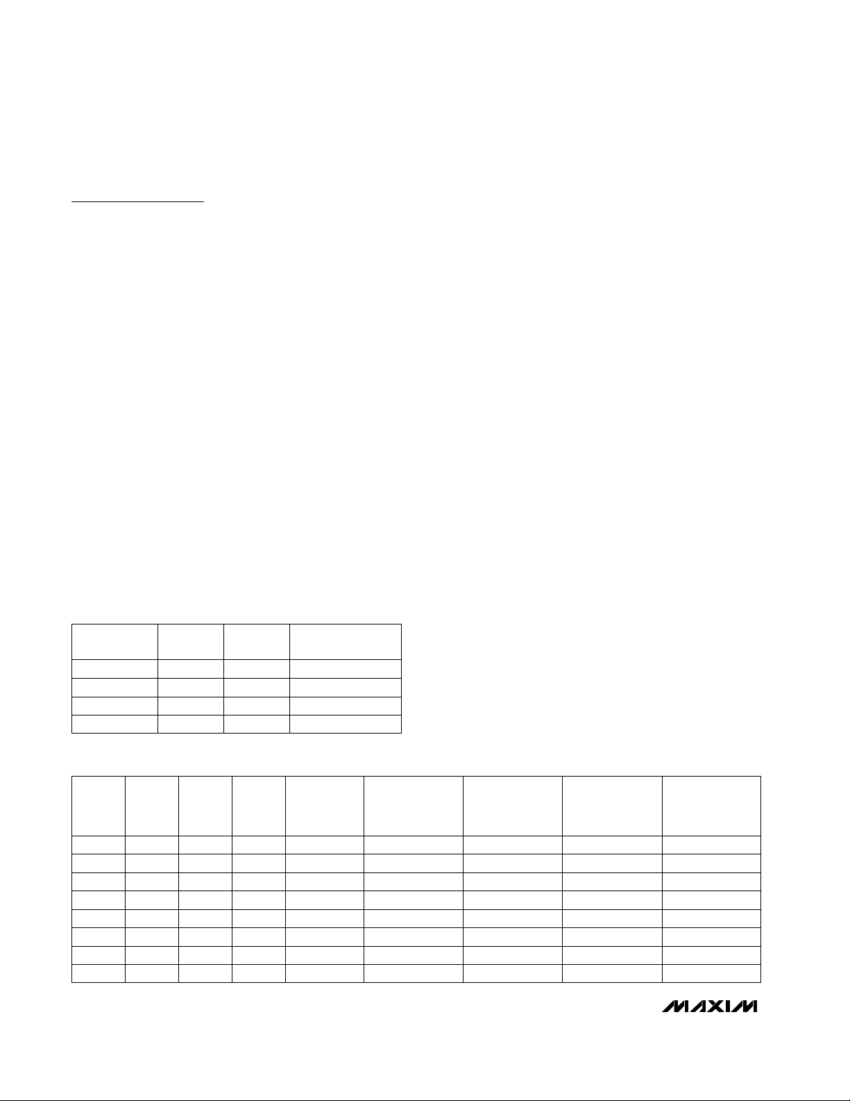
DAC and the coarse gain of the PGA (Tables 1 and 2).
These bits must be properly configured for the optimum
dynamic range of the ADC. The digitized sensor signal
is stored in a read-only DSP register.
The on-chip temperature sensor also has a 3-bit
coarse-offset DAC that places the temperature signal in
the ADC operating range. Digitized temperature is also
stored in a read-only DSP register. The DSP uses the
digitized sensor, the temperature signals, and the correction coefficients to calculate the compensated and
corrected output.
The MAX1460 supports an automated production environment, where a test system communicates with a
batch of MAX1460s and controls temperature and sen-
sor excitation. The three-state digital outputs on the
MAX1460 allow parallel connection of transducers, so
that all five serial interface lines (XIN, TEST, RESET,
SDIO, and SDO) can be shared. The test system
selects an individual transducer using CS1 and CS2.
The test system must vary the sensor’s input and temperature, calculate the correction coefficients for each
unit, load the coefficients into the MAX1460 nonvolatile
EEPROM, and test the resulting compensation.
The MAX1460 DSP implements the following characteristic equation:
where Gain corrects the sensor’s sensitivity, G
1
and G
2
correct for Gain-TC, T and Signal are the digitized outputs of the analog front end, Of0corrects the sensor’s
offset, Of1and Of2correct the Offset-TC, and D
OFF
is
the output offset pedestal.
The test system can write the calibration coefficients
into the MAX1460 EEPROM or write to the DSP registers directly. The MAX1460 can begin a conversion
using either the EEPROM contents or the register contents. When the test system issues commands, the
MAX1460 is a serially controlled slave device.
The test system observes the MAX1460 DSP operation
in order to acquire the temperature and signal ADC
results, to verify the calibration coefficients, and to get
the output D. The MAX1460 places the contents of several important DSP registers on the serial interface after
the tester issues a Start Conversion command.
After calibration, compensation, and final test, the
MAX1460 is adapted to its sensor and the pair can be
removed from the test system. Use the resulting trans-
93113
77012
61101
46000
NOMINAL GAIN
(V/V)
PGA-0PGA-1
PGA SETTING
1
(mV RTI)
(V
DD
= 5V)
CO-0CO-1CO-S
PGA SETTING
3
(mV RTI)
(V
DD
= 5V)
PGA SETTING
2
(mV RTI)
(V
DD
= 5V)
PGA SETTING
0
(mV RTI)
(V
DD
= 5V)
% V
DD
(at ADC
input)
CO
SETTING
122
79
39
8097162110+3 149
010+2 52
100+1
6210496
25315147
-4
4
-39
-79
-122
-3-3-5-5
3355
-25-31-47
-52-62
-104
-96
-80-97-162-149
000+0
001-0
101-1
011-2
111-3
Table 2. Typical Coarse Offset DAC Settings
Table 1. Nominal PGA Gain Settings
PGA
SETTING
-51
D Gain 1 G T G T
=++
()
1
Signal Of Of T Of T D
++ +
01 22OFF
2
2
+

MAX1460
Low-Power, 16-Bit Smart ADC
_______________________________________________________________________________________ 7
ducer by applying power and the START signal. Latch
the 12-bit parallel digital output using the EOC pulse.
The maximum conversion rate of the MAX1460 is 15Hz,
using a 2MHz resonator. If an analog output is desired,
build a simple lowpass filter using the OUT pin, the
uncommitted op amp, and a few discrete components
(Figure 8).
Analog Front End, Including PGA, Coarse
Offset DAC, ADC, and Temperature Sensor
Before the sensor signal is digitized, it must be gained
and coarse-offset corrected to maximize the ADC
dynamic range. There are 2 bits (four possible settings)
in the configuration register for the PGA gain, and 3 bits
(eight possible settings) for the CO DAC. The flowchart
(Figure 1) shows a procedure for finding the optimum
Figure 1. Flowchart for Determining PGA and CO Settings
–MAKE A TEST SYSTEM VARIABLE CALLED “NoMoreGain.”
–SET THE TEMPERATURE TO WHERE THE SENSOR’S SENSITIVITY IS HIGHEST. THIS IS NORMALLY COLD FOR SILICON PRTs.
–SET THE PGA GAIN SETTINGS TO MINIMUM.
–CLEAR THE VARIABLE “NoMoreGain.”
–APPLY MIDSCALE EXCITATION TO THE SENSOR.
–FIND THE COARSE OFFSET DAC SETTING WHERE THE DIGITIZED SIGNAL REGISTER IS CLOSEST TO ZERO (MIDSCALE).
–APPLY MAXIMUM SENSOR EXCITATION.
–TEST FOR CLIPPING (DIGITIZED SIGNAL > 0.85).
DID ADC CLIP?
YES YES
IS THE PGA AT
MINIMUM GAIN?
–APPLY MINIMUM SENSOR EXCITATION.
–TEST FOR CLIPPING (DIGITIZED SIGNAL < -0.85).
THE SENSOR SENSITIVITY
IS TOO LARGE. ADD A
RESISTOR BETWEEN THE
TOP OF THE BRIDGE
, THEN
AND V
DD
START OVER.
V
DD
SERIES
RESISTOR
NO NO
–REDUCE THE PGA GAIN ONE STEP.
–SET THE VARIABLE “NoMoreGain.”
IS THE PGA AT
MAXIMUM GAIN?
YES YES
CAUTION: CLIPPING IS STILL POSSIBLE FOR LARGE SENSOR’S OFFSET TC AND LARGE TEMPERATURE RANGES.
IF NECESSARY, GUARDBAND AGAINST CLIPPING BY REDUCING THE ±0.85 CLIPPING CONSTANTS ABOVE.
NO
IS “NoMoreGain” SET?
RECORD THE PGA AND COARSE OFFSET SETTINGS.
NO
SENSOR
INCREASE THE PGA GAIN ONE STEP.
MAX1460
Low-Power, 16-Bit Smart ADC
8 _______________________________________________________________________________________
analog front-end settings when the sensor’s characteristics are unknown. Use the tabulated values (Tables 1
and 2) if the peak sensor excursions are known. See
the Test System Interface section for details on writing
these analog front-end bits.
The PGA gain and the CO are very stable, but are not
accurate. Manufacturing variances on the gain and offset of the MAX1460 analog front-end superposition the
residual sensor errors, and are later removed during
final calibration.
For example, suppose the sensor’s sensitivity is
+10mV/V with an offset of -12mV/V. Let the supply volt-
age be +5V. The full scale (-FS) output of the sensor is
then +5V(-12mV/V) = -60mV; +FS is then +5V (-12mV/V
+ 10mV/V) = -10mV. Following through the flowchart,
the PGA gain setting is +3 (gain = 93V/V) and the CO
correction setting is +1 (+25mV RTI) - (Referred-to
Input). The coarsely corrected -FS input to the ADC is
(-60mV + 25mV)93 = -3.255V. The +FS input to the
ADC is (-10mV + 25mV)93 = +1.395V. The input range
of the ADC is ±VDD. Thus the maximum and minimum
digitized sensor signals become -3.255 / 5 = -0.651
and +1.395 / 5 = +0.279.
Notice that the bridge multiplies the signal by VDDand
the ADC divides the signal by VDD. Thus, the system is
ratiometric and not dependent on the DC value of VDD.
The ADC output clips to ±1.0 when input values exceed
±V
DD
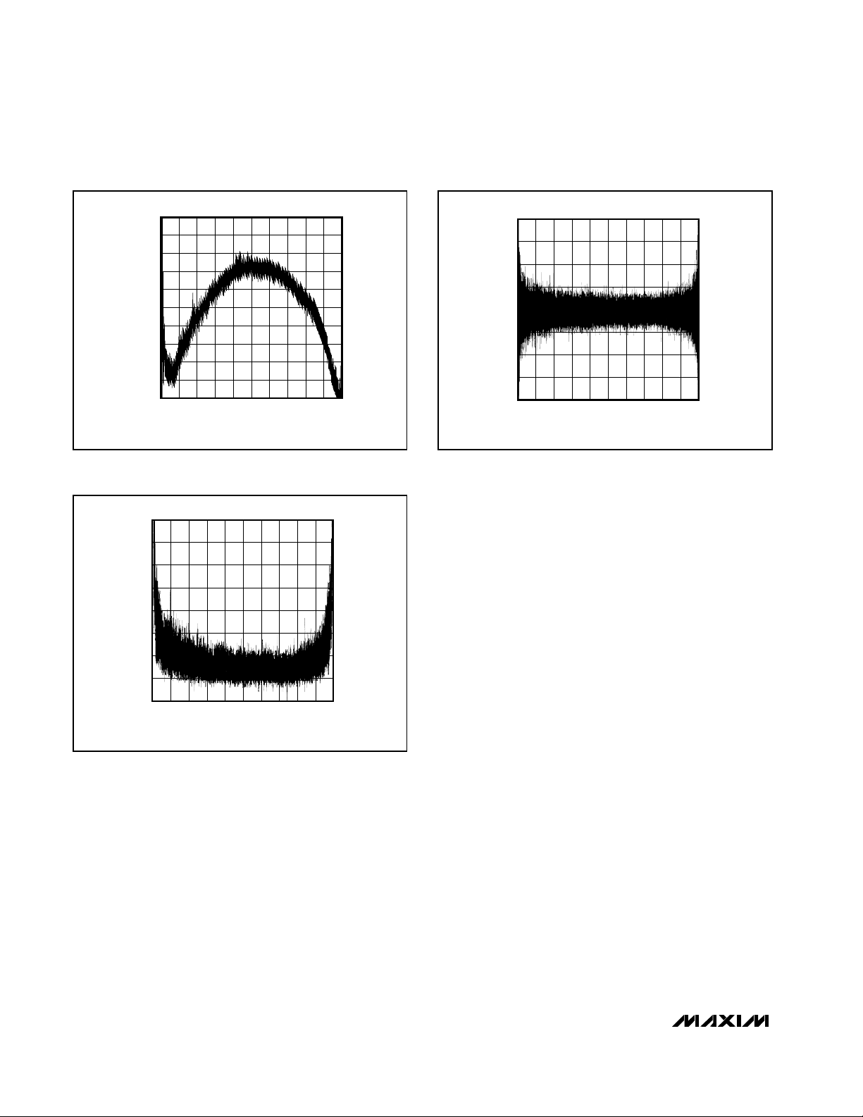
. The best signal-to-noise ratio (SNR) is achieved
when the ADC input is within ±85% of V
DD
(Figure 2).
The MAX1460 includes an internal temperature-sensing
bridge allowing the MAX1460 temperature to be used
as a proxy for the sensor temperature. For this reason,
the MAX1460 must be mounted in thermal proximity to
the sensor. The output of the temperature-sensing
bridge is also corrected by a 3-bit coarse-offset DAC
and processed by the ADC. The selection of the
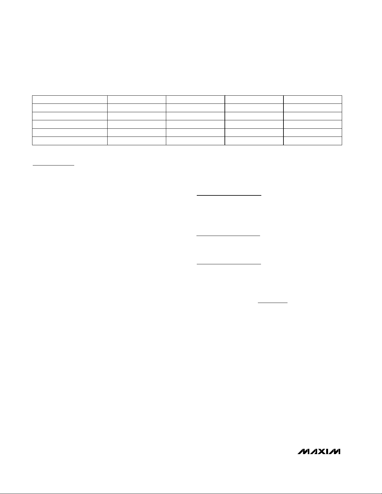
Temperature Sensor Offset (TSO) bits in the configuration register should be made so that the digitized temperature signal is as close to 0.0 as possible at
midscale temperature. This is done to maximize the
dynamic range of the thermal-calibration coefficients
(Table 3).
Figure 2a. Analog Front-End INL (typical)
Figure 2b. Analog Front-End Differential Nonlinearity (DNL)
(typical)
Figure 2c. Analog Front-End Noise Standard Deviation of the
Samples (typical)
0.010
0.008
0.006
0.004
0.002
0
-0.002
0.004
NONLINEARITY ERROR (%FS)
-0.006
-0.008
-0.010
-100 -60 -40 -20-80 0 20 40 8060 100
SENSOR SIGNAL INPUT OR ADC INPUT/OUTPUT RANGE (%)
4.0
3.5
3.0
2.5
2.0
1.5
1.0
0.5
NOISE STANDARD DEVIATION (16-BIT LSBs)
0
-100 -60 -40 -20 0-80 20 40 60 80 100
SENSOR SIGNAL INPUT OR ADC INPUT/OUTPUT RANGE (%)
4
3
2
1
0
-1
ERROR (16-BIT LSBs)
-2
-3
-4
-100 -20-40-80 -60 0 20 40 60 80 100
SENSOR SIGNAL INPUT OR ADC INPUT RANGE (%)

MAX1460
Low-Power, 16-Bit Smart ADC
_______________________________________________________________________________________ 9
Test-System Interface: Writing Calibration
Coefficients to the DSP Registers
and EEPROM
To make the MAX1460 respond to commands from the
test system, raise the TEST pin and drive XIN with a
2MHz clock signal. It is not necessary to remove the
resonator. RESET must be low for at least 16 clock
cycles to initialize the MAX1460. Then, a rising transi-
tion on RESET begins a 32-bit serial transfer of the testsystem command word through SDIO. The test system
transitions SDIO on falling edges of the XIN clock; the
MAX1460 latches data is on the rising edge (Figure 3).
The 32-bit command word generated by the test-system is divided into four fields (Figure 3). The 4-bit command field is interpreted in Table 4. The other fields are
usually ignored, except that command 1 hex uses the
two register fields, and command 2 hex requires an
EEPROM address. The command word fields are:
• Register Data Field: Holds the calibration coefficients to be written into the MAX1460 16-bit registers
• EEPROM Address Field: Holds the hexadecimal
address of the EEPROM bit to be set (from 00 hex to
7F hex)
• Register Address Field: Contains the address of the
register (0 to 7) where the calibration coefficient is to
be written
• Command Field: Instructs the MAX1460 to take a
particular action (Table 4)
Figure 3. Test-System Command Timing Diagram
TSO-0TSO-1TSO-2
TEMPERATURE
BRIDGE
OFFSET
TSO
SETTING
1117
0116
1015
Minimum
–
–
–
–
–
–
Maximum
0014
1103
0102
1001
0000
Table 3. Temperature Sensor Offset
(TSO) Settings
MIN
16 CLK
CYCLES
XIN
TEST
RESET
SDIO
D0 D1 D2 D3 D4 D5 D6 D7 D8 D9
NOTE: ALL TRANSITIONS MUST OCCUR WITHIN 100ns OF THE XIN CLOCK EDGE.
00 01 02 03 29 30 31 00 01 02 03 29 30 31 00 01 02 03 29 30 31 00 01 02 03 29 30 31
D0 D1 D2 D3 C3
COMMAND 1
NU
NU D0 D1 D2 D3 C3
REGISTER DATA FIELD
COMMAND 2 COMMAND 3 COMMAND n
D10 D11 D12 D13
NU
NU D0 D1 D2 D3 C3
D14
D15 E0 E1 E2 E3 E4 E5 E6 R0 R1 R2 C0 C1 C2 C3 NU NU
MSB LSBLSB MSB LSB MSB LSB MSB
EEPROM ADDRESS
FIELD
NU
NU D0 D1 D2
REG.
ADD
D3 C3 NU
COMMAND
NU

MAX1460
Low-Power, 16-Bit Smart ADC
10 ______________________________________________________________________________________
Writing to the DSP Registers
Command 1 hex writes calibration coefficients from the
test system directly into the DSP registers. Tester commands 8 hex and C hex cause the MAX1460 to start a
conversion using the calibration coefficients in the registers. This direct use of the registers speeds calibration and compensation because it does not require
EEPROM write-access time. Bringing RESET low clears
the DSP registers, so the test system should always
write to the registers and start a conversion in a single
command timing sequence.
As shown in Table 5, seven registers hold the calibration coefficients of the characteristic equation [D
OUT
=
Gain (1+G1T + G2T2) (Signal + Of0+ Of1T + Of2T2) +
D
OFF
] implemented by the MAX1460 DSP. All of the
registers are 16-bit, two’s complement coding format.
When a register is interpreted as an integer, the decimal range is from -32768 (8000 hex) to +32767 (7FFF
hex). Fractional coefficient values range from -1.0
(8000 hex) to +0.99997 (7FFF hex).
The register at address 0 is called the Configuration
Register. It holds the coarse offset, PGA gain, Op Amp
Power-Down, temperature-sensor offset, repeat mode,
and reserved bits, as shown in Table 6. The functionality of the coarse offset, PGA gain, and temperature-sensor bits are described in the Analog Front End section.
The Op Amp Power-Down bit enables the uncommitted
op amp when set. The repeat-mode bit is tested by the
last instruction of the DSP microcode, and, if set, immediately initiates another conversion cycle. The Maxim
reserved bits should not be altered.
Write a calibration coefficient into a DSP register. 1
0
1 hex
4 hex
0
0 0 0
0
2 hex
0 hex
0
0
8 hex
Block-Erase the entire EEPROM (writes “0” to all 128 bits). 0 1 0
A hex
Write “1” to a single EEPROM bit. 0 0 1
0
NOOP (NO-OPeration) 0 0 0
0
Start Conversion command. The registers are not updated with EEPROM values.
SDIO and SDO are enabled as DSP outputs.
1 0 0
C hex
E hex
C0HEX CODE
Reserved 3, 5, 6, 7, 9, B, D, F hex
- - - -
Start Conversion command. The registers are updated with EEPROM values. SDIO
and SDO are enabled as DSP outputs.
1 0 1
Start Conversion command. The registers are not updated with EEPROM values.
SDIO and SDO are disabled.
1 1 0
Start Conversion command. The registers are updated with EEPROM values. SDIO
and SDO are disabled.
1 1 1
COMMAND C3 C2 C1
Table 4. Test System Commands
Gain
6
7
1
2
Of
2
Gain correction -32768 to +32767 Integer
Quadratic TC offset
3
4
-1.0 to +0.99997 Fraction
D
OFF
G
1
Linear TC gain -1.0 to +0.99997 Fraction
Output midscale pedestal
G
2
Quadratic TC gain -1.0 to +0.99997 Fraction
-32768 to +32767
Of
0
Offset correction -1.0 to +0.99997 Fraction
Integer
REGISTER
ADDRESS
Of
1
5 Linear TC offset -1.0 to +0.99997 Fraction
COEFFICIENT FUNCTION RANGE FORMAT
Table 5. DSP Calibration Coefficient Registers

MAX1460
Low-Power, 16-Bit Smart ADC
______________________________________________________________________________________ 11
Writing to the Internal EEPROM
The test system writes to the EEPROM with commands
4 hex (Block-Erase the entire EEPROM), 2 hex (Write
“1” to a single EEPROM bit) and 0 hex (NOOP). During
normal operation (when the TEST pin is low) or when
the test system issues instructions A hex or E hex (Start
conversion from EEPROM values), the DSP reads the
Calibration Coefficients from the EEPROM.
In the normal production flow, determine the calibration
coefficients using direct register access. Then load the
calibration coefficients into the EEPROM with tester
instruction 2 hex. Instruction 4 hex block-erases the
EEPROM and is necessary only for a rework or reclaim
operation. For each part, the Maxim reserved bits in the
Configuration Register should be read before instruction 4 hex is issued, and restored afterwards. The
MAX1460 is shipped with its internal EEPROM uninitialized, except for the reserved bits.
The internal 128-bit EEPROM is arranged as eight 16bit words. These eight words are the configuration
register and the seven calibration-coefficient values
(Table 7).
The MAX1460 EEPROM is bit addressable. The final calibration coefficients must be mapped into the
EEPROM locations that are to be set. There is no bitclear instruction. Any EEPROM write operation is neces-
sarily long because the internal charge pump must create and maintain voltages above 20V long enough to
cause a reliably permanent change in the memory.
Writing an EEPROM bit requires 6ms, so writing the
EEPROM typically requires less than 400ms. Do not
decrease the EEPROM write times.
To write an EEPROM bit, the test system must be compliant with the Command Timing Diagram shown in Figure
3, performing the following operations:
1) Issue command 0 hex, including the EEPROM
address field of the bit to be written.
2) Issue command 2 hex, with the address field used in
step 1. Continuously repeat this command 375 times
(6ms).
3) Issue command 0 hex, including the EEPROM
address field used in steps 1 and 2.
The procedure for using command 4 hex (Block-Erase
the EEPROM) is similar. Record the Maxim Reserved
bits in the configuration register prior to using this command, and restore them afterwards. The number of
Block-Erase operations should not exceed 100.
1) Issue command 0 hex.
2) Issue command 4 hex. Continuously repeat this
command 375 times (6ms).
3) Issue command 0 hex.
Test System Interface:
Observing the DSP Operation
Test system commands 8 hex and A hex initiate a conversion while allowing the test system to observe the
operation of the DSP. To calibrate a unit, the test system must know the digitized temperature and sensor
signals, stored in DSP registers 8 and 9, and the calibrated and compensated output stored in DSP register
10. The test system should also verify the EEPROM con-
tents, registers 0–7. All these signals pass through DSP
register S during the execution of the instruction ROM
microcode. The SDO pin outputs the S register values,
and the SDIO pin tells the tester which signal is currently
on S.
01 CO-0 (LSB)
09 Maxim Reserved
TSO-0 (LSB)
CO-1 (MSB)
0 (LSB)
8
TSO-1
0A 9
0B
CO-S (Sign)
10
TSO-2 (MSB)
02 1
0C 11
0D
03 2
12 Maxim Reserved
PGA-1 (MSB)04 3
Maxim Reserved
Maxim Reserved
0E
05 4
13
0F 14
Repeat Mode
PGA-0 (LSB)
10 15 (MSB)
Maxim Reserved
Maxim Reserved
06 5
07 6
Op Amp Power-Down
08 7
EEPROM
ADDRESS
(HEX)
DESCRIPTION
BIT
POSITION
Table 6. Configuration Register Bitmap

MAX1460
Low-Power, 16-Bit Smart ADC
12 ______________________________________________________________________________________
There are three internal DSP registers that are directly
observable on the SDIO and SDO pins:
• S: 16-bit DSP Scratch or Accumulator register, con-
taining the result of the execution of the current
microcode instruction.
• P: 8-bit DSP Program Pointer register, which holds
the address of the instruction ROM microcode.
• PS: 8-bit DSP Program Store register. PS is the
instruction that the DSP is currently executing. PS is
the instruction ROM data at address P.
The DSP instructions relevant to the test system are listed in Table 8.
After the test system sends the Start Conversion commands 8 hex or A hex, SDIO and SDO are both
enabled as MAX1460 serial outputs. The test system
should disable (high impedance) its SDIO driver to
avoid a bus conflict at this time so that the MAX1460
can drive the pin. After the DSP executes each one of
the microcode instructions, the contents of the registers
S, P, and PS are output in a serial format (Figure 4).
A new DSP instruction and a new state of the S, P, and
PS registers are delivered every 16n + 9 clock cycles,
where n = 0, 1, 2... after the Start Conversion command
completes. The tester should latch the SDIO and SDO
0F
MSB Configuration LSB
0D0E
1F
MSB
0B
Gain LSB
EE Address (hex) 10
1D
09
Contents
1E
0A
1BEE Address (hex) 20 19
Contents
1A
0C
1C 18 16
08
17 14 12
06
1315 11
07
2F
MSB G
1
04
LSB
2D
02
2E
03
3F
MSB
05
2B
G
2
LSB
01
EE Address (hex) 30
3D
29
Contents
3E
2A
3BEE Address (hex) 40 39
Contents
3A
2C
3C 38 36
28
37 34 32
26
3335 31
27 24 222325 21
4F
MSB Of
0
LSB
4D4E
5F
MSB
4B
Of
1
LSB
EE Address (hex) 50
5D
49
Contents
5E
4A
5BEE Address (hex) 60 59
Contents
5A
4C
5C 58 56
48
57 54 52
46
5355 51
47
6F
MSB Of
2
44
LSB
6D
42
6E
43
7F
MSB
45
6B
D
OFF
LSB
41
EE Address (hex) 70
7D
69
Contents
7E
6A
7BEE Address (hex) 00 79
Contents
7A
6C
7C 78 76
68
77 74 72
66
7375 71
67 64 626365 61
Table 7. EEPROM Memory Map
D7 Register 7—D
OFF
Register 8—Temperature
Signal
Register 0—Configuration
56
Register 9—Sensor Signal
D8 01
D9
Register 1—Gain
3B
Register 10—Compensated
Output D
D0 66 or 6C
EA 65 or 6B
D1 47
Register 2—G
1
D2 11
D3 2E Register 3—G
2
Register 4—Of
0
Register 5—Of
1
D4 38
D5 03
Register 6—Of
2
D6 22
INSTRUCTION
CODE (PS)
(HEX)
S REGISTER VALUE
PROGRAM
COUNTER
(P)
(HEX)
Table 8. Subset of DSP Instruction

MAX1460
Low-Power, 16-Bit Smart ADC
______________________________________________________________________________________ 13
Figure 4. DSP Serial Output Timing Diagram
bits on the falling edge of the XIN clock signal. When
the P and PS registers in Table 8 appear on SDIO, the
tester should save the corresponding SDO data.
The conversion timing of the MAX1460 is shown in
Figure 5 and Table 9. In the figure, the conversion is
initiated by a rising transition on the START pin.
Equivalently, conversion can be initiated in TEST mode
after completion of tester commands 8 hex or A hex, or
reinitiated by the state of the Repeat Mode bit in the
configuration register. After a conversion is initiated,
the 16-bit ADC digitizes the temperature and sensor
signals during t
ADC
. Then, the DSP executes the
instruction ROM microcode during t
DSP
. In TEST mode,
and during t
DSP
, SDIO and SDO outputs carry useful
information. At 130,586 clock cycles after the Start
Conversion command is received, the LSB of the S and
P DSP registers is available on SDO and SDIO. The last
DSP instruction is D0 hex. The tester can now start a
new communication sequence by lowering the RESET
pin for at least 16 clock cycles, and then resume driving SDIO. SDIO becomes high impedance when
RESET is low.
Figure 5. MAX1460 Conversion Timing
th
CLOCK CYCLE (16 (n + 1) + 9)th CLOCK CYCLE
(16 n + 9)
XIN
LSB
SDO
S12 S13 S14 S15
SDIO
PS4 PS5 PS6 PS7 P0 P1 P2 P3 P4 P5 P6 P7 PS0 PS1
DSP CYCLE n-1 DSP CYCLE n DSP CYCLE n+1
NOTE: ALL TRANSITIONS MUST OCCUR WITHIN 100ns OF THE XIN CLOCK EDGE.
S0 S1 S2 S3 S4 S5 S6 S7 S8 S9
LSB LSBMSB
V
DD
t
WARM
START
(OPTIONAL)
MSB
S10 S11 S12 S13 S14 S15 S0 S1 S2 S3 S4 S5 S6 S7 S8 S9 S10 S11
MSB
PS2 PS3 PS4 PS5 PS6 PS7 P0 P1 P2 P3 P4 P5 P6 P7 PS0 PS1 PS2 PS3
t
CONV
t
ADC
SDIO & SDO
(TEST MODE)
D [11...0]
EOC
t
DSP
t
EOC
MAX1460
Low-Power, 16-Bit Smart ADC
14 ______________________________________________________________________________________
Applications Information
Calibration and Compensation Procedure
Perform fine calibration by characterizing the sensor/
MAX1460 pair using the test system and then finding
the calibration coefficients Gain, G1, G2, Of0, Of1, and
Of
2
using the equations below. This simple fine-calibration procedure requires three temperatures, denoted A,
B, and C, and two sensor excitations, named S and L
for small and large. Thus, there are six data points (AS,
AL, BS, BL, CS, and CL); six unknown calibration coefficients; and six versions of the characteristic equation, in
the form:
Equation (1)
where DL, DS, and D
OFF
are determined by the end
product specification. D
L
is the desired MAX1460 output corresponding to the L sensor excitation; DSis the
desired MAX1460 output corresponding to the S sensor excitation; D
OFF
is the desired midscale output;
SignalCLis the digitized sensor reading at temperature
C with the L sensor excitation applied; and TCis the
digitized temperature reading at temperature C.
Unstable digitized temperature readings indicate that
thermal equilibrium has not been achieved, necessitating increased soak times or a better thermal control.
Averaging many readings from the MAX1460 will help
filter out AC variations in the sensor excitation and oven
temperature.
Begin calibration by soaking the sensor and the
MAX1460 pair at the first temperature, A, and apply the
L excitation to the sensor. Start a conversion and
record the digitized temperature TAand the digitized
signal SignalAL. Apply the S sensor excitation, and
record the digitized signal SignalAS. Repeat this procedure for temperatures B and C, recording TB, SignalBL,
SignalBS, TC, SignalCL, and SignalCS.
The A
L
and ASversions of equation 1 may be ratioed to
obtain:
Equation (2a)
Similarly,
Equation (2b)
Equation (2c)
where
Equation (3)
Equations 2a, 2b, and 2c form a system of three linear
equations, with three unknowns, Of
0
, Of1, and Of2.
Solve for Of
0
, Of1, and Of2.
The small sensor excitation versions of Equation 1 can
be ratioed to obtain:
Equation (4a)
Equation (4b)
Y Y G TY TY
G TY TY 0
CS BS 1 B CS C BS
2B2CS C2BS
−
()
+−
()
+
−
=
Table 9. MAX1460 Conversion Timing
PARAMETER SYMBOL MIN MAX UNITS
Sensor Warm-Up Time t
WARM
35
—
ms
ADC Time t
ADC
130,585 130,585 XIN clk cycles
DSP Time t
DSP
3,220 3,364 XIN clk cycles
EOC Pulse Width t
EOC
8 8 XIN clk cycles
Conversion Time t
CONV
133,805 133,949 XIN clk cycles
Signal x Signal
−
⋅
AL AS
1x
−
Signal x Signal
−
⋅
BL BS
1x
−
Of Of T Of T 0
++ + =
01A2A
Of Of T Of T 0
++ + =
01B2B
D D Gain 1 G T G T
−= ++
L OFF 1 C 2 C
Signal Of Of T Of T
++ +
CL 0 1 C 2 C
2
2
Signal x Signal
−
⋅
CL CS
1x
−
x
=
Of Of T Of T 0
++ + =
01C2C
DD
−
L OFF
DD
−
S OFF
YY G TYTY
−
()
CS AS 1 A CS C AS
G T Y T Y 0
2A2CS C2AS
+−
()
−
=
2
2
2
+

MAX1460
Low-Power, 16-Bit Smart ADC
______________________________________________________________________________________ 15
where:
Equation (5a)
Equation(5b)
Equation (5c)
Equations 4a and 4b form a system of two linear equations and two unknowns, G1and G2. Solve for G1and
G2. Equation 1 can now be readily solved for the last
unknown, Gain.
Arithmetic manipulation can magnify measurement
errors and noise. Quantization of the calibration coefficients is another reason to consider adjusting the Gain
and D
OFF
coefficients. To do this, load the MAX1460
registers with the calculated coefficients Gain, G1, G2,
Of0, Of1, Of2, and D
OFF
. Assuming the oven is still at
temperature C and the S sensor excitation is still
applied, measure the output DCS. Change to the L sensor excitation, and measure D
CL
. Compute the new
Gain coefficient using equation 6. Remeasure DCL, and
compute the new D
OFF
coefficient, given by equation
7.
Equation (6)
Equation (7)
The final calibration coefficients may now be written
into the MAX1460 EEPROM. The unit is now ready for
final test.
Figure 6. Sensor Characteristics Before Compensation
Figure 7. Compensated Sensor/MAX1460 Pair
Figure 8. Filtering the Output DAC
UNCOMPENSATED SENSOR ERROR
10
8
6
4
2
0
-2
ERROR (%FSO)
-4
-6
-8
-10
0 10203040506070
TEMPERATURE (°C)
COMPENSATED TRANSDUCER ERROR
0.20
0.15
0.10
0.05
0
-0.05
-0.10
ERROR (% SPAN, 4000 CODES)
-0.15
-0.20
02010 30 40 50 60 70
FSO
OFFSET
TEMPERATURE (°C)
FSO
OFFSET
Y
AS
Y
BS
=
Signal Of Of T Of T
=
Signal Of Of T Of T
DD
−
S OFF
++ +
AS 0 1 A 2 A
DD
−
S OFF
++ +
BS 0 1 B 2 B
2
2
CF
1µF
R
MAX1460
OP AMP
500k
F
AMPOUT
FILTERED
ANALOG
OUTPUT
2
V
DD
OUT
AGND
Y
CS
UNFILTERED
BITSTREAM
=
R
D1
10k
R
D2
10k
R1
500k
AMP-
AMP+
DD
S OFF
Signal Of Of T Of T
++ +
CS 0 1 C 2 C
−
GAIN Gain
DDDD
new
OFF
=
new
DD
−
LS
DD
−
CL CS
=+−
OFF L CL

MAX1460
Low-Power, 16-Bit Smart ADC
16 ______________________________________________________________________________________
This algorithm minimizes the error directly at the six test
conditions, AS, AL, BS, BL, CS, and CL. Space the
temperatures A, B, and C widely to minimize the signalto-noise ratio of the measurement. If there is a large
error remaining in the finished product, move the calibration temperatures closer to the peak error temperatures. Similarly, full-scale sensor excitation may not be
the best calibration condition if the sensor has nonlinearities. Move S and L away from full scale.
Figure 6 shows the characteristics of an individual
Lucas-NovaSensor model NPH8-100-EH, 0 to 15psig,
silicon pressure sensor. Figure 7 shows the result of the
compensated sensor/MAX1460 pair.
Using the Compensated
Sensor/MAX1460 Pair
After calibration and removal from the test system, the
MAX1460 and the sensor form a mated pair. The START
pin can be connected to VDDor left unconnected if the
sensor does not require a significant warm-up time. Now
operation is simple: just apply power and latch the parallel output D when EOC falls. Temperature is digitized during the first half of t
ADC
, so the MAX1460 provides a
minimum sensor warm-up time of 35ms. Using a 2MHz
resonator, the conversion time t
CONV
is nominally 67ms. If
the Repeat Mode bit is set, conversions repeat at a rate of
15Hz.
If the sensor requires more than 35ms of warm-up time,
the START pin may be used to initiate conversion (Figure
5). If the Repeat Mode bit is set, START should remain
high. If the Repeat Mode bit is reset, START may be used
to externally control the conversion rate of the MAX1460.
After the 12-bit parallel output D is latched, end the conversion by taking START low for at least one clock cycle.
The output DAC converts the parallel digital output into
a serial bitstream on OUT. A simple external lowpass
filter, using the MAX1460 op amp, converts the OUT
bitstream into a ratiometric analog voltage (Figure 8).
The filter shown is an inverting configuration, but the
Gain and D
OFF
coefficients of the characteristic equa-
tion can be adjusted to obtain either polarity. If the op
amp is not used, it can be powered down using the Op
Amp Power-Down bit in the configuration register.
The MAX1460 requires a minimum of external components:
• One power-supply bypass capacitor (C1) from V
DD
to VSS.
• One 2MHz ceramic resonator (X1).
• Two 10kΩ resistors for the AGND pin.
• If an analog output is desired, two 500kΩ resistors
and a 1µF capacitor are needed for filtering.
MAX1460 Evaluation/
Development Kit
The MAX1460 evaluation kit (EV kit) speeds the development of MAX1460-based transducer prototypes and
test systems. First-time users of the MAX1460 are
strongly encouraged to use this kit, which includes:
1) Evaluation board, with a MAX1460 sample and a silicon pressure sensor, ready for customer evaluation.
2) Interface board that must be connected to a PC parallel port.
3) MAX1460 communication/compensation software
(Windows compatible), which enables programming
of the MAX1460 one module at a time.
4) Detailed Design/Applications manual, developed for
sensor-test engineers.
The evaluation kit order number is MAX1460EVKIT.
Pin Configuration
XIN
SDO
XOUT
RESET
V
EOC
DDVDD
24
D0
37
36
N.C.
35
AMP-
34
AMP+
33
AMPOUT
N.C.
32
N.C.
31
OUT
30
D5
29
D4
28
D3
27
D2
26
D1
25
N.C.
N.C.
AGND
START
I.C.
D10
D11
N.C.
INM
TEST
INP
N.C.
N.C.
N.C.
N.C.
N.C.
4847464544434241403938
1
2
3
4
5
6
D6
7
D7
D8
8
D9
9
10
11
12
1314151617181920212223
N.C.
MAX1460
SS
DD
V
V
CS1
CS2
N.C.
N.C.
SDIO

MAX1460
Low-Power, 16-Bit Smart ADC
______________________________________________________________________________________ 17
Functional Diagram
Chip Information
TRANSISTOR COUNT: 59,855
SUBSTRATE CONNECTED TO V
SS
C1
0.1µF
SENSOR
+5V
10k
10k
2MHz RESONATOR
X
1
+5V
XIN
XOUT
V
DD
INP
INM
AGND
MAX1460
OSCILLATOR
PGA &
COARSE
OFFSET
CORRECTION
CS1 CS2 START TEST RESET SDIO SDO EOC AMP- AMP+
16-BIT INTERFACE TO ALL SIGNALS
TEMPERATURE
SENSOR
MUX
CONTROL
LOGIC
16-BIT ADC
REF = V
DD
EEPROM
CONFIGURATION
REGISTER
CORRECTION
COEFFICIENTS
REGISTERS
TEMPERATURE &
SENSOR SIGNAL
REGISTERS
INSTRUCTION
ROM
16-BIT
DIGITAL SIGNAL
PROCESSOR
(DSP)
OP
AMP
REF = V
DAC
12-BIT DIGITAL OUTPUT
V
SS
AMPOUT
DD
OUT
D [11...0]

MAX1460
Low-Power, 16-Bit Smart ADC
18 ______________________________________________________________________________________
NOTES

MAX1460
Low-Power, 16-Bit Smart ADC
______________________________________________________________________________________ 19
NOTES

MAX1460
Low-Power, 16-Bit Smart ADC
Maxim cannot assume responsibility for use of any circuitry other than circuitry entirely embodied in a Maxim product. No circuit patent licenses are
implied. Maxim reserves the right to change the circuitry and specifications without notice at any time.
20 ____________________Maxim Integrated Products, 120 San Gabriel Drive, Sunnyvale, CA 94086 408-737-7600
© 1999 Maxim Integrated Products Printed USA is a registered trademark of Maxim Integrated Products.
NOTES
 Loading...