

For free samples and the latest literature, visit www.maxim-ic.com or phone 1-800-998-8800.
For small orders, phone 1-800-835-8769.
General Description
The MAX1459 highly integrated analog-sensor signal
conditioner is optimized for piezoresistive sensor calibration and compensation with minimal external components. It includes a programmable current source for
sensor excitation, a 3-bit programmable-gain amplifier
(PGA), a 128-bit internal EEPROM, and four 12-bit DACs.
Achieving a total error factor within 1% of the sensor’s
repeatability errors, the MAX1459 compensates offset,
offset temperature coefficient (offset TC), full-span output
(FSO), FSO temperature coefficient (FSOTC), and FSO
nonlinearity of silicon piezoresistive sensors.
The MAX1459 calibrates and compensates first-order
temperature errors by adjusting the offset and span of
the input signal through digital-to-analog converters
(DACs), thereby eliminating quantization noise.
The MAX1459 allows temperature compensation via the
external sensor, an internal temperature-dependent
resistor, or a dedicated external temperature transducer. Accuracies better than 0.5% can be achieved with
low-cost external temperature sensors (i.e., silicon transistor), depending on sensor choice.
Built-in testability features on the MAX1459 result in the
integration of three traditional sensor-manufacturing
operations into one automated process:
• Pretest: Data acquisition of sensor performance
under the control of a host test computer.
• Calibration and compensation: Computation and
storage (in an internal EEPROM) of calibration and
compensation coefficients computed by the test
computer and downloaded to the MAX1459.
• Final test operation: Verification of transducer cali-
bration and compensation without removal from the
pretest socket.
Although optimized for use with piezoresistive sensors,
the MAX1459 may also be used with other resistive
sensors (i.e., accelerometers and strain gauges) with
some additional external components.
________________________Applications
4–20mA Transmitters
Piezoresistive Pressure and Acceleration
Industrial Pressure Sensors
Load Cells/Wheatstone Bridges
Strain Gauges
Temperature Sensors
Features
♦ Highly Integrated Sensor Signal Conditioner for
2-Wire, 4–20mA Transmitters
♦ Sensor Errors Trimmed Using Correction
Coefficients Stored in Internal EEPROM—
Eliminates the Need for Laser Trimming and
Potentiometers
♦ Compensates Offset, Offset TC, FSO, FSOTC,
FSO Linearity
♦ Programmable Current Source (0.1mA to 2.0mA)
for Sensor Excitation
♦ Fast Signal-Path Settling Time (≈1ms)
♦ Accepts Sensor Outputs from +1mV/V to +40mV/V
♦ Fully Analog Signal Path
♦ Internal or External Temperature Reference
Compensation
♦ Automated Pilot Production (Calibration/
Compensation) System Available
♦ Write Protection for EEPROM Data Security
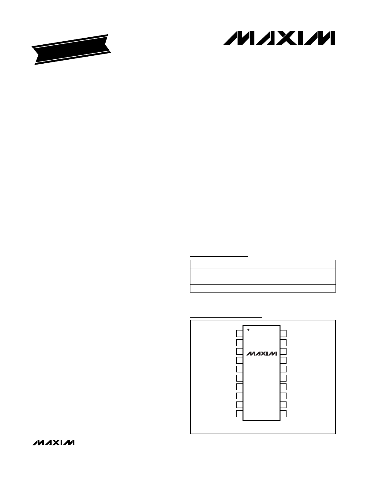
Pin Configuration
Ordering Information
MAX1459
2-Wire, 4–20mA
Smart Signal Conditioner
________________________________________________________________ Maxim Integrated Products 1
19-1619; Rev 0; 1/00
*Dice are tested at TA= +25°C, DC parameters only.
Functional Diagram appears at end of data sheet.
EVALUATION KIT
AVAILABLE
20 SSOP
Dice*
20 SSOP
PIN-PACKAGETEMP. RANGE
0°C to +70°C
0°C to +70°C
-40°C to +125°CMAX1459AAP
MAX1459C/D
MAX1459CAP
PART
For custom versions of the MAX1459, see the Customization
section at end of data sheet.
TOP VIEW
FSOTC
AMP+
AMPOUT
TEMPIN
1
SCLK V
CS
2
DIO
3
MAX1459
4
WE
5
6
AMP-
7
8
9
ISRC
10
SSOP
20
NBIAS
19
CK50
18
TEMP2
17
TEMP1
16
INM
15
INP
14
BDRIVE
13
12
V
OUT
11
DD
SS

MAX1459
2-Wire, 4–20mA
Smart Signal Conditioner
2 _______________________________________________________________________________________
ABSOLUTE MAXIMUM RATINGS
Stresses beyond those listed under “Absolute Maximum Ratings” may cause permanent damage to the device. These are stress ratings only, and functional
operation of the device at these or any other conditions beyond those indicated in the operational sections of the specifications is not implied. Exposure to
absolute maximum rating conditions for extended periods may affect device reliability.
Supply Voltage, VDDto VSS......................................-0.3V to +6V
All Other Pins ...................................(V
SS
- 0.3V) to (VDD+ 0.3V)
Short-Circuit Duration, FSOTC, OUT, BDRIVE ...........Continuous
Continuous Power Dissipation (T
A
= +70°C)
20-Pin SSOP (derate 8.00mW/°C above +70°C) ..........640mW
Operating Temperature Ranges
MAX1459CAP ......................................................0°C to +70°C
MAX1459AAP .................................................-40°C to +125°C
Storage Temperature Range .............................-65°C to +150°C
Lead Temperature (soldering, 10s) .................................+300°C
ELECTRICAL CHARACTERISTICS
(VDD= +5V, VSS= 0, TA= +25°C, unless otherwise noted.)
PARAMETER
SYMBOL MIN TYP MAX UNITS
Amplifier Gain Nonlinearity 0.01 %V
DD
Input-Referred Offset Tempco ±0.5 µV/°C
Input Impedance R
IN
1 MΩ
Output Step Response 2 ms
Common-Mode Rejection Ratio CMRR 90 dB
Input-Referred Adjustable Offset
Range
±150 mV
Supply Voltage V
DD
4.5 5.0 5.5 V
Supply Current I
DD
2.0 2.5 mA
Input-Referred Adjustable FullSpan Output (FSO) Range
+1 to +40 mV/V
Differential Signal Gain Range +41 to +230 V/V
Minimum Differential Signal Gain +36 +41 +44 V/V
Differential Signal Gain Tempco ±50 ppm/°C
Output Current Range
-0.45 0.45
(sink) (source)
mA
Output Noise 500 µV
RMS
CONDITIONS
(Note 5)
(Notes 2, 3)
63% of final value
Selectable in eight steps
TA= T
MIN
to T
MAX
From VSSto V
DD
At minimum gain (Note 4)
TA= T
MIN
to T
MAX
V
OUT
= (VSS+ 0.25V) to (VDD- 0.25V)
DC to 10Hz (gain = 41,
source impedance = 5kΩ)
R
NBIAS
= 402kΩ, VDD= 5.0V (Note 1)
Output Voltage Swing
V
SS
+ 0.05 VDD- 0.05
V
No load
V
SS
+ 0.25 VDD- 0.2510kΩ load
GENERAL CHARACTERISTICS
ANALOG INPUT (PGA)
ANALOG OUTPUT (PGA)
Bridge Current Range I
BDRIVE
0.1 0.5 2.0 mA
Bridge Voltage Swing V
BDRIVE
V
SS
+ 1.3 VDD- 1.3 VI
BDRIVE
= 2mA
Reference Input Voltage Range
(ISRC)
V
ISRC
V
SS
+ 1.3 VDD- 1.3 V
CURRENT SOURCE

ELECTRICAL CHARACTERISTICS (continued)
(VDD= +5V, VSS= 0, TA= +25°C, unless otherwise noted.)
MAX1459
2-Wire, 4–20mA
Smart Signal Conditioner
_______________________________________________________________________________________ 3
FSO DAC Bit Weight
∆V
ISRC
∆Code
1.22 mV/bit
FSOTC DAC Bit Weight
∆V
FSOT
∆Code
0.6 mV/bit
DAC reference = VDD= 5.0V
DAC reference = V
BDRIVE
= 2.5V
Offset DAC Bit Weight
∆V
OUT
∆Code
2.8 mV/bit
Offset TC DAC Bit Weight
∆V
OUT
∆Code
1.4 mV/bit
DAC reference = VDD= 5.0V
DAC reference = V
BDRIVE
= 2.5V
DAC Resolution 12 Bits
Differential Nonlinearity DNL ±1.5 LSB
PARAMETER SYMBOL MIN TYP MAX UNITS
DAC Bit Weight 9 mV/bit
DAC Resolution 3 Bits
Output Voltage Swing 0.2 4.0 V
Current Drive -20 20 µA
Current Source Reference
Resistor
R
ISRC
100 kΩ
FSO Trim Resistor R
FTC
100 kΩ
Temperature-Dependent
Resistor
R
TEMP
100 kΩ
CONDITIONS
Input referred, VDD= 5V (Note 6)
No load, VB= 5V
V
FSOTC
= 2.5V
Input Common-Mode Range CMR V
SS
V
DD
V
Open-Loop Gain A
V
60 dB
Offset Voltage (as unity-gain
follower)
-30 30 mVVIN= VDD/2
Output Swing VSS+ 0.05 V
DD -
0.05 VNo load
Output Current ±1 mA
DIGITAL-TO-ANALOG CONVERTERS
IRO DAC
FSOTC BUFFER (FSOTC Pin)
INTERNAL RESISTORS
AUXILIARY OP AMP
MAX1459
2-Wire, 4–20mA
Smart Signal Conditioner
4 _______________________________________________________________________________________
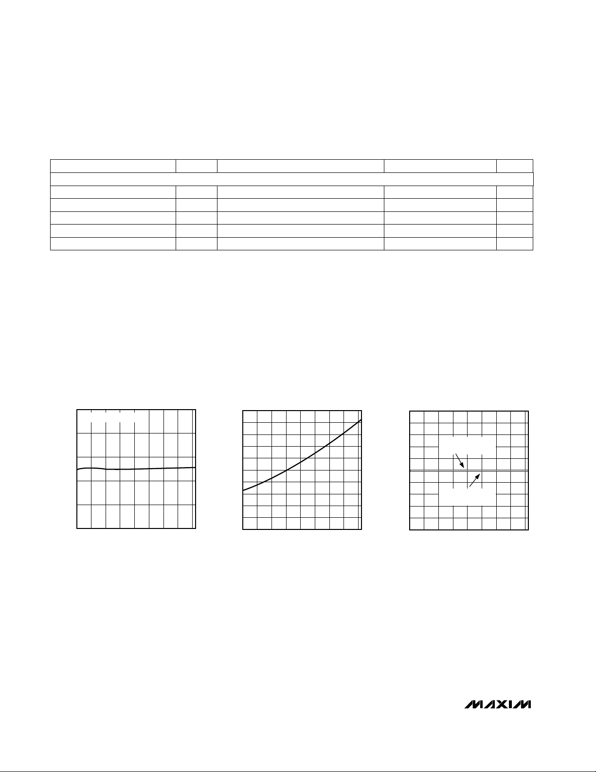
__________________________________________Typical Operating Characteristics
(VDD= +5V, VSS= 0, TA= +25°C, unless otherwise noted.)
0
0.5
1.0
1.5
2.0
2.5
-40 40 60020-20 80 100 120
SUPPLY CURRENT vs. TEMPERATURE
MAX1459 toc01
TEMPERATURE (°C)
SUPPLY CURRENT (mA)
V
OUT
= 2.47V AT +25°C
-40 40 60020-20 80 100 120
R
TEMP
vs. TEMPERATURE
MAX1459 toc02
TEMPERATURE (°C)
R
TEMP
(Ω)
0
60
40
20
80
100
120
140
160
180
200
-40 40 60020-20 80 100 120
V
OUT
vs. TEMPERATURE
MAX1459 toc03
TEMPERATURE (°C)
V
OUT
(V)
0
1.5
1.0
0.5
2.0
2.5
3.0
3.5
4.0
4.5
5.0
V
OUT
= 2.5V AT +25°C
V
IN
= 56.5mV
V
OUT
= 2.47V AT +25°C
V
IN
= 0
Note 1: Excludes the sensor or load current.
Note 2: All electronics temperature errors are compensated together with sensor errors.
Note 3: The sensor and the MAX1459 must always be at the same temperature during calibration and use.
Note 4: This is the maximum allowable sensor offset.
Note 5: This is the sensor’s sensitivity normalized to its drive voltage, assuming a desired full-span output of 4V and a bridge
voltage of 2.5V. Sensors smaller than +10mV/V require an auxiliary op amp.
Note 6: Bit weight is ratiometric to V
DD
.
ELECTRICAL CHARACTERISTICS (continued)
(VDD= +5V, VSS= 0, TA= +25°C, unless otherwise noted.)
I
SINK
= 2mA V0.5V
OL
Low-Level Output Voltage
I
SOURCE
= 1mA V4V
OH
High-Level Output Voltage
V2Input Hysteresis
V0.25 x V
DD
V
IL
Low-Level Input Voltage
V0.75 x V
DD
V
IH
High-Level Input Voltage
CONDITIONS UNITSMIN TYP MAXSYMBOLPARAMETER
DIGITAL PINS

MAX1459
2-Wire, 4–20mA
Smart Signal Conditioner
_______________________________________________________________________________________ 5
Temperature Sensor Terminal 1TEMP116
Temperature Sensor Terminal 2. R
TEMP
is a 100kΩ temperature-dependent resistor with 4600ppm/°C
tempco.
TEMP217
Output Voltage. OUT is a Rail-to-Rail®output that can drive resistive loads down to 10kΩ and capacitive
loads up to 0.1µF.
OUT11
Negative Power Supply V
SS
12
Sensor Excitation Current Output. The current source that drives the bridge.BDRIVE13
Positive Sensor Input. Input impedance is typically 1MΩ. Rail-to-rail input range.INP14
Negative Sensor Input. Input impedance is typically 1MΩ. Rail-to-rail input range.INM15
Auxiliary Op Amp Negative InputAMP-7
Auxiliary Op Amp OutputAMPOUT8
Input pin for an External Temperature-Dependent Reference Voltage for FSOTC DAC and OTC DAC. In the
default mode, the MAX1459 uses the temperature-dependent bridge drive voltage as the FSOTC DAC and
OTC DAC reference.
TEMPIN9
Current Source Reference. An internal 100kΩ resistor (R
ISRC
) connects ISRC to VSS(see Functional
Diagram). Optionally, external resistors can be used in place of or in parallel with R
FTC
and R
ISRC
.
ISRC10
Auxiliary Op Amp Positive InputAMP+6
Buffered Full-Span Output Temperature Coefficient DAC Output. An internal 100kΩ resistor (R
FTC
) connects FSOTC to ISRC (see Functional Diagram). Optionally, external resistors can be used in place of or in
parallel with R
FTC
and R
ISC
.
FSOTC5
Write Enable, Dual-Function Input Pin. Used to enable EEPROM erase/write operations. Also used to set
the DAC refresh-rate mode. Internally pulled to VDDwith a 1MΩ (typ) resistor. See the Chip-Select (CS)
and Write-Enable (WE) section.
WE4
Data Input/Output. Used only during programming/testing. Internally pulled to VSSwith a 1MΩ (typical)
resistor. High impedance when CS is low.
DIO3
Positive Power-Supply Input. Connect a 0.1µF capacitor from VDDto VSS.V
DD
20
Clock Output, nominally 50kHzCK5018
Chip Current Bias Source. Connect an external 402kΩ ±1% resistor between VDDand NBIAS.NBIAS19
Pin Description
1
Chip-Select Input. The MAX1459 is selected when this pin is high. When low, OUT and DIO become high
impedance. Internally pulled to V
DD
with a 1MΩ (typical) resistor. Leave unconnected for normal operation.
CS2
Data Clock Input. Used only during programming/testing. Internally pulled to VSSwith a 1MΩ (typical) resistor.
Data is clocked in on the rising edge of the clock. Recommended SCLK frequency is below 50kHz.
SCLK
PIN FUNCTIONNAME
Rail-to-Rail is a registered trademark of Nippon Motorola, Ltd.
MAX1459
_______________Detailed Description
The MAX1459 provides an analog amplification path for
the sensor signal and a digital path for calibration and
temperature correction. Calibration and correction is
achieved by varying the offset and gain of a programmable-gain amplifier (PGA) and by varying the sensor
bridge current. The PGA utilizes a switched-capacitor
CMOS technology, with an input-referred offset trimming range of ±63mV (9mV steps). An additional output-referred fine offset trim is provided by the offset
DAC (approximately 2.8mV steps). The PGA provides
eight gain values from +41V/V to +230V/V. The bridge
current source is programmable from 0.1mA to 2mA.
The MAX1459 uses four 12-bit DACs with calibration
coefficients stored by the user in an internal 128-bit
EEPROM. This memory contains the following information as 12-bit-wide words:
• Configuration register
• Offset calibration coefficient
• Offset temperature error compensation coefficient
• Full-span output (FSO) calibration coefficient
• FSO temperature error compensation coefficient
• 24 user-defined bits for customer programming of
manufacturing data (e.g., serial number and date)
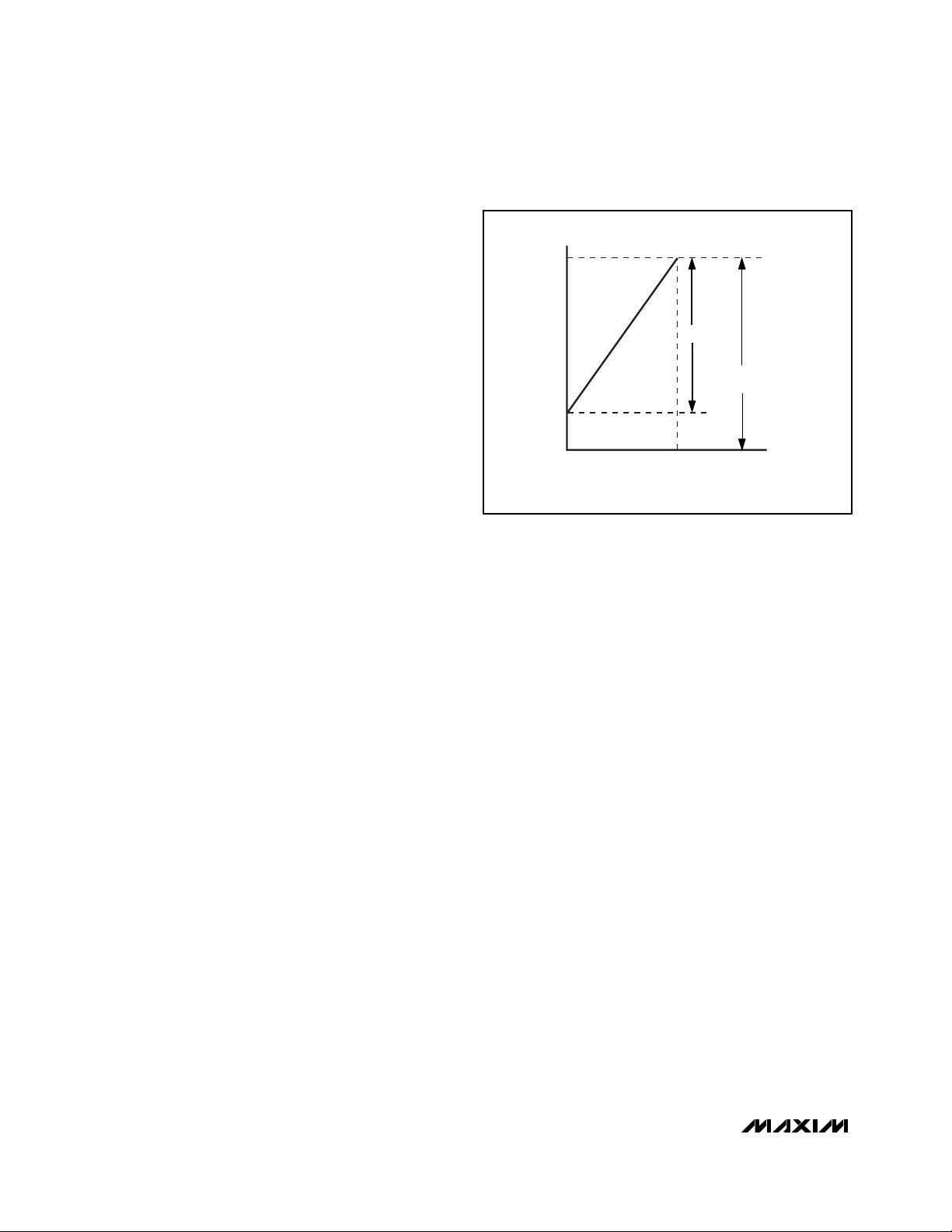
Figure 1 shows a typical pressure-sensor output and
defines the offset, full-scale, and FSO values as a function of voltage.
FSOTC Compensation
Silicon piezoresistive transducers (PRTs) exhibit a large
positive input resistance tempco (TCR) so that, while
under constant current excitation, the bridge voltage
(V
BDRIVE
) increases with temperature. This depen-
dence of V
BDRIVE
on the sensor temperature can be
used to compensate the sensor temperature errors.
PRTs also have a large negative full-span output sensitivity tempco (TCS) so that, with constant voltage excitation, FSO will decrease with temperature, causing a
full-span output temperature coefficient (FSOTC) error.
However, if the bridge voltage can be made to increase
with temperature at the same rate that TCS decreases
with temperature, the FSO will remain constant.
FSOTC compensation is accomplished by resistor
R
FTC
and the FSOTC DAC, which modulate the excitation reference current at ISRC as a function of temperature (Figure 2). FSO DAC sets V
ISRC
and remains
constant with temperature while the voltage at FSOTC
varies with temperature. FSOTC is the buffered output
of the FSOTC DAC. The reference DAC voltage is
V
BDRIVE
, which is temperature dependent. The FSOTC
DAC alters the tempco of the current source. When the
tempco of the bridge voltage is equal in magnitude and
opposite in polarity to the TCS, the FSOTC errors are
compensated and FSO will be constant with temperature.
OFFSET TC Compensation
Compensating offset TC errors involves first measuring
the uncompensated offset TC error, then determining
what percentage of the temperature-dependent voltage
V
BDRIVE
must be added to the output summing junction
to correct the error. Use the offset TC DAC to adjust the
amount of BDRIVE voltage that is added to the output
summing junction (Figure 3).
Analog Signal Path
The fully differential analog signal path consists of four
stages:
• Front-end summing junction for coarse offset correction
• 3-bit PGA with eight selectable gains ranging from
41 through 230
• Three-input-channel summing junction
• Differential to single-ended output buffer with rail-to-
rail output (Figure 3)
Coarse Offset Correction
The sensor output is first fed into a differential summing
junction (INM (negative input) and INP (positive input))
with a CMRR > 90dB, an input impedance of approximately 1MΩ, and a common-mode input voltage range
from V
SS
to VDD. At this summing junction, a coarse off-
set-correction voltage is added, and the resultant volt-
2-Wire, 4–20mA
Smart Signal Conditioner
6 _______________________________________________________________________________________
Figure 1. Typical Pressure-Sensor Output
4.5
FULL-SPAN OUTPUT (FSO)
P
MAX
FULL-SCALE (FS)
VOLTAGE (V)
0.5
OFFSET
P
MIN
PRESSURE
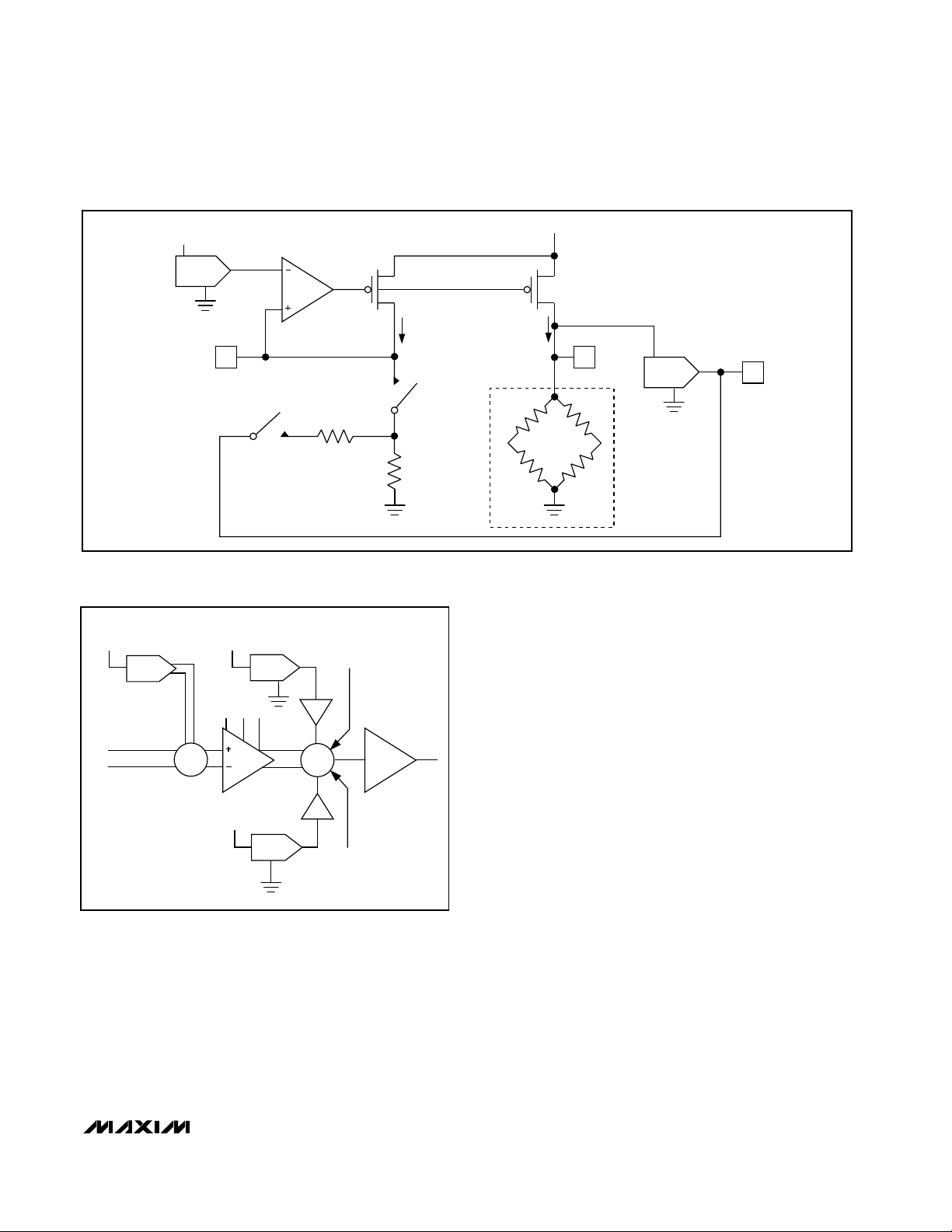
age is fed into the PGA. The 3-bit (plus sign) inputreferred offset DAC (IRO DAC) generates the coarse
offset-correction voltage. The DAC voltage reference is
1.25% of VDD; thus, a VDDof 5V results in a front-end
offset-correction voltage ranging from -63mV to +63mV,
in 9mV steps (Table 1). To add an offset to the input
signal, set the IRO sign bit high; to subtract an offset
from the input signal, set the IRO sign bit low. The IRO
DAC bits (C2, C1, C0, and IRO sign bit) are programmed in the configuration register (see Internal
EEPROM section).
Programmable-Gain Amplifier
The programmable-gain amplifier (PGA), which is used
to set the coarse FSO, uses a switched-capacitor
CMOS technology and contains eight selectable gain
levels from 41 to 230, in increments of 27 (Table 2). The
output of the PGA is fed to the output summing junction. The three PGA gain bits A2, A1, and A0 are stored
in the configuration register.
Output Summing Junction
The third stage in the analog signal path consists of a
summing junction for the PGA output, offset correction,
and the offset TC correction. Both the offset and the offset TC correction voltages are gained by a factor of 2.3
before being fed into the summing junction, increasing
the offset and offset TC correction range. The offset sign
bit and offset TC sign bit are stored in the configuration
register. The offset sign bit determines whether the offset correction voltage is added to (sign bit is high) or
subtracted from (sign bit is low) the PGA output.
Negative offset TC errors require a logic high for the offset TC sign bit. Alternately, positive offset TC errors dictate a logic low for the offset TC sign bit. The output of
the summing junction is fed to the output buffer.
MAX1459
2-Wire, 4–20mA
Smart Signal Conditioner
_______________________________________________________________________________________ 7
Figure 2. Bridge Excitation Circuit
Figure 3. Signal-Path Block Diagram
V
V
DD
FSO
DAC
DD
I = I
ISRC
I
SRC
R
FTC
R
ISRC
1.25% V
DD
IRO
DAC
INP
INM
BDRIVE
A2
V
A1 A0
PGA
DD
OFFTC
DAC
OFFSET
DAC
A = 2.3
A = 2.3
SOTC
±
OUT
ΣΣ
A = 1
±
SOFF
AA ≈ 12I
= I
ISRC
EXTERNAL
SENSOR
BDRIVE
BDRIVE
FSOTC
DAC
FSOTC

MAX1459
Output Buffer
The output buffer (OUT) can swing within 50mV of the
supply rails with no load, or within 0.25V of either rail
while driving a 10kΩ load. OUT can easily drive 0.1µF
of capacitance. The output is current limited and can
be shorted to either V
DD
or VSSindefinitely. If CS is
brought low, OUT goes high impedance, resulting in
typical output impedance of 1MΩ. This feature allows
parallel MAX1459 connections, reducing test system
wire harness complexity.
Bridge Drive
Fine FSO correction is accomplished by varying the
sensor excitation current with the 12-bit FSO DAC
(Figure 2). Sensor bridge excitation is performed by a
programmable current source capable of delivering up
to 2mA. The reference current at ISRC is established by
resistor R
ISRC
and by the voltage at node ISRC (con-
trolled by the FSO DAC). The reference current flowing
through this pin is multiplied by a current mirror (AA ≅
12) and then made available at BDRIVE for sensor excitation. Modulation of this current with respect to temperature can be used to correct FSOTC errors, while
modulation with respect to the output voltage (V
OUT
)
can be used to correct FSO linearity errors.
Voltage Drive Sensor
For sensors with negligible FSOTC, the MAX1459 can
be configured as a fixed-voltage drive by shorting ISRC
and BDRIVE. Offset TC can then be compensated with
R
TEMP
. Set configuration register bit 5 to 1, and connect TEMPIN to a temperature-dependent voltage
source. This source can easily be generated by inducing a current through R
TEMP
. For more information on
this application, refer to the MAX1459 Reference Manual.
Digital-to-Analog Converters
The four 12-bit, sigma-delta DACs typically settle in
less than 100ms. The four DACs have a corresponding
memory register in EEPROM for storage of correction
coefficients.
The FSO DAC takes its reference from VDDand controls V
ISRC
, which sets the baseline sensor excitation
current. The FSO DAC is used for fine adjustments to
the FSO. The offset DAC also takes its reference from
VDDand provides a 1.22mV resolution with a VDDof
5V. The output of the offset DAC is fed into the output
summing junction where it is gained by approximately
2.3, which increases the resulting output-referred offset-correction resolution to 2.8mV.
Both the offset TC and FSOTC DACs take their references from a temperature-dependent voltage. In
default mode, this voltage is internally connected to
BDRIVE. Alternatively, a different temperature sensor
can be used through TEMPIN by setting bit 5 of the
configuration register. This temperature sensor can be
either R
TEMP
or an external temperature resistor.
2-Wire, 4–20mA
Smart Signal Conditioner
8 _______________________________________________________________________________________
2.0702301117
1.8272030116
1.5841761015
1.3411490014
1.0981221103
0.855950102
0.612681001
0.369
OUTPUTREFERRED IRO
DAC STEP SIZE
(VDD= 5V) (V)
41
PGA
GAIN
(+V/+V)
0
PGA
VALUE
A0A2
000
A1
Table 2. PGA Gain Settings and IRO DAC
Step Size
0 0
-63-1.251110-7
-54-1.080110-6
-45-0.901010-5
-36-0.720010-4
-27-0.541100-3
-18-0.360100-2
-9-0.181000-1
0000-0
+9+0.181001+1
+18+0.360101+2
+27+0.541101+3
+36+0.720011+4
+45+0.901011+5
+54+1.080111+6
VALUE C0
C2 C1SIGN
+63
OFFSET
CORREC-
TION AT
V
DD
= 5V
(mV)
+1.25
OFFSET
CORREC-
TION
PERCENT
OF V
DD
(%)
1
IRO DAC
111+7
Table 1. Input-Referred Offset DAC
Correction Values

The offset TC DAC output is fed into the output summing junction where it is gained by approximately 2.3,
thereby increasing the offset TC correction range. The
buffered FSOTC DAC output is available at FSOTC and
is connected to ISRC via R
FTC
to correct FSOTC errors.
Internal Resistors
The MAX1459 contains three internal resistors (R
ISRC
,
R
FTC
, and R
TEMP
) optimized for common silicon PRTs.
R
ISRC
(in conjunction with the FSO DAC) programs the
nominal sensor excitation current. R
FTC
(in conjunction
with the FSOTC DAC) compensates the FSOTC errors.
Both R
ISRC
and R
FTC
have a nominal value of 100kΩ. If
external resistors are used, R
ISRC
and R
FTC
can be
disabled by setting the appropriate bit (address 07h
reset to zero) in the configuration register (Table 3).
R
TEMP
is a high-tempco resistor with a TC of
+4600ppm/°C and a nominal resistance of 100kΩ at
+25°C. This resistor can be used with certain sensor
types that require an external temperature sensor. The
two R
TEMP
terminals are available as pin 16 and pin 17
of the MAX1459.
Internal EEPROM
The MAX1459 has a 128-bit internal EEPROM arranged
as eight 16-bit registers. The 4 uppermost bits for each
register are reserved. The internal EEPROM is used to
store the following (also shown in the memory map in
Table 4):
• Configuration register (Table 3)
• 12-bit calibration coefficients for the offset and FSO
DACs
• 12-bit compensation coefficients for the offset TC
and FSOTC DACs
• Two general-purpose registers available to the user
for storing process information such as serial number, batch date, and check sums
The EEPROM is bit addressable. Program the EEPROM
using the following steps, where the bits have addresses from 0 to 127 (07F hex):
1) Read the entire EEPROM, and temporarily store the
reserved bits.
2) Erase the entire EEPROM, which causes all bits to
be 0 (see the ERASE EEPROM Command section).
3) Program 1 to the required bits, including the reserved
bits (see the WRITE EEPROM BIT Command section).
4) Read the whole EEPROM, either with the READ EEPROM BIT or with the READ EEPROM MATRIX commands (see the READ EEPROM BIT Command and
READ EEPROM MATRIX Command sections).
Configuration Register
The configuration register (Table 3) determines the
PGA gain, the polarity of the offset and offset TC coefficients, and the coarse offset correction (IRO DAC). It
also enables/disables internal resistors (R
FTC
and
R
ISRC
).
DAC Registers
The offset, offset TC, FSO, and FSOTC registers store
the coefficients used by their respective calibration/
compensation DACs.
Detailed Description of the Digital Lines
Chip-Select (CS) and Write-Enable (WE)
CS is used to enable OUT, control serial communication, and force an update of the configuration and DAC
registers:
• A low on CS disables serial communication and
places OUT in a high-impedance state.
• A transition from low to high on CS forces an update
of the configuration and DAC registers from the
MAX1459
2-Wire, 4–20mA
Smart Signal Conditioner
_______________________________________________________________________________________ 9
Table 3. Configuration Register
Description
011
00
03
0
3
022
055
04
07
4
7
066
09
BIT
9
EEPROM
ADDRESS (hex)
08
0B
8
11
0A10
Offset TC Sign Bit, SOTC
Offset Sign Bit, SOFF
PGA Gain (LSB), A0
PGA Gain, A1
PGA Gain (MSB), A2
Temperature Sensor Selection Bit
(0 = default V
BDRIVE
)
Reserved “0”
R
ISRC/RFTC
Selection Bit
(0 = enable internal), IRS
IRO LSB, C0
IRO, C1
IRO MSB, C2
IRO Sign, S
IRO
DESCRIPTION
CONFIGURATION REGISTER

MAX1459
EEPROM when the U bit of the INIT sequence is
zero.
• A transition from high to low on CS terminates pro-
gramming mode.
• A logic high on CS enables OUT and serial commu-
nication (see Communication Protocol section).
WE controls the refresh rate for the internal configuration and DAC registers from the EEPROM and enables
the erase/write operations. If communication has been
initiated (see Communication Protocol section), internal
register refresh is disabled.
• A low on WE disables the erase/write operations and
also disables register refreshing from the EEPROM.
• A high on WE selects a refresh rate of approximately
400 times per second and enables EEPROM
erase/write operations.
• It is recommended that WE be connected to V
SS
after the MAX1459 EEPROM has been programmed.
SCLK (Serial Clock)
SCLK must be driven externally and is used to input
commands to the MAX1459 or program the internal
EEPROM contents. Input data on DIO is latched on the
rising edge of SCLK.
2-Wire, 4–20mA
Smart Signal Conditioner
10 ______________________________________________________________________________________
Table 4. EEPROM Memory Map
EE Address
Contents
EE Address
Contents
EE Address
Contents
EE Address
Contents
EE Address
Contents
Reserved
EE Address
Contents
EE Address
Contents
0E
0
0C
0
0F 0D
0
0A 080B 09 06 0407 05 02
1
00
Configuration
03 01
1E
0
1C
1
1F 1D
0
1A 181B 19 16 1417 15 12
1
10
MSB Offset LSB
13 11
2E
0
2C
0
2F 2D
1
2A 282B 29 26 2427 25 22
1
20
MSB Offset TC LSB
23 21
3E
0
3C
1
3F 3D
1
3A 383B 39 36 3437 35 32
1
30
MSB FSO LSB
33 31
4E
1
4C
0
4F 4D
0
4A 484B 49 46 4447 45 42
1
40
MSB FSOTC LSB
43 41
6E
0
6C
0
6F 6D
0
6A 686B 69 66 6467 65 62
0
60
User-Defined Bits
63 61
7E
0
7C
0
7F 7D
0
7A 787B 79 76 7477 75 72
0
70
User-Defined Bits
73 71
Note: The MAX1459 processes the Reserved Bits in the EEPROM. If these bits are not properly programmed, the configuration
and DAC registers will not be updated correctly.
= Reserved Bits
5153 50
0
525557 5456595B 585A
0
5D5F
0
5C
0
5E
Reserved

Data Input/Output
The DIO line is an input/output pin used to issue commands to the MAX1459 (input mode) or read the
EEPROM contents (output mode).
In input mode (the default mode), data on DIO is
latched on each rising edge of SCLK. Therefore, data
on DIO must be stable at the rising edge of SCLK and
should transition on the falling edge of SCLK.
DIO will switch to output mode after receiving either the
READ EEPROM command or the READ EEPROM
MATRIX command. See the Read EEPROM section for
detailed information.
Communication Protocol
To initiate communication, the first 8 bits on DIO after
CS transitions from low to high must be 101010U0 (AA
hex or A8 hex, defined as the INIT sequence). The
MAX1459 will then begin accepting 16-bit control
words (Figure 4).
If the INIT SEQUENCE is not detected, all subsequent
data on DIO is ignored until CS again transitions from
low to high and the correct INIT SEQUENCE is received.
The U bit of the INIT SEQUENCE controls the updating
of the DACs and configuration register from the internal
EEPROM. If this bit is low (U = 0, INIT SEQUENCE = A8
hex), all four internal DACs and the configuration regis-
ter will be updated from the EEPROM on the next rising
edge of CS (this is also the default on power-up). If the
U bit is high (INIT SEQUENCE = AA hex), the DACs
and configuration register will not be updated from the
internal EEPROM; they will retain their current value on
any subsequent CS rising edge. The MAX1459 continues to accept control words until CS is brought low.
Control Words
After receiving the INIT SEQUENCE on DIO, the
MAX1459 begins latching in 16-bit control words, MSB
first (Figure 5).
The first 4 bits of the control word (the MSBs,
CM3–CM0) are the command field. The last 12 bits
(D11–D0) represent the data field. The MAX1459 supports the commands listed in Table 5.
No-OP Command (0 hex)
The no-operation (No-OP) command must be issued
before and after the commands ERASE EEPROM and
WRITE EEPROM BIT. In the case of the ERASE EEPROM command, the control word must be 0000 hex. In
the case of the WRITE EEPROM BIT command, the
command field must be 0h, and the data field must
have, in its lower bits, the EEPROM address to be written (Figure 6). For example, to write location 1C hex of
MAX1459
2-Wire, 4–20mA
Smart Signal Conditioner
______________________________________________________________________________________ 11
Figure 5. Control-Word Timing Diagram
Figure 4. Communication Sequence
CS
t
= 1.5ms
MIN
SCLK
DIO
X
SCLK
COMMAND
MSB LSB LSBMSB
CM3
DIO
CM2
MSB LSB
8 CLK
CYCLES
1
0
CM1
1
CM0
0
1 CM3
0U0
INIT
SEQUENCE
D11
D9D6D8D5D7
D10
16-BIT CONTROL WORD
16 CLK
CYCLES
CM2
CONTROL
WORD
DATA
16 CLK
CYCLES
CM3
CM2DODO
CONTROL
WORD
D4
D3 D2 D1 D0
n x 16 CLK
CYCLES
CONTROL
WORDS

MAX1459
the EEPROM (one of the reserved bits), the necessary
commands are:
• 001C hex: No-OP command, with address 1C hex
in the data field
• 201C hex: WRITE EEPROM BIT command, with
address 1C hex in the data field
• 001C hex: No-OP command, with address 1C hex
in the data field
ERASE EEPROM Command (1 hex)
When an ERASE EEPROM command is issued, all of
the memory locations in the EEPROM are reset to a
logic 0. The data field of the 16-bit word is ignored
(Figure 7).
Important: An internal charge pump develops voltages
greater than 20V for EEPROM programming operations.
The EEPROM control logic requires 10ms to erase the
EEPROM. After sending a write or erase command, failure to wait 10ms before issuing another command may
result in unreliable EEPROM operation. The maximum
number of EEPROM ERASE cycles should not exceed 100.
WRITE EEPROM BIT Command (2 hex)
The WRITE EEPROM BIT command stores a logic high
at the memory location specified by the lower 7 bits of
the data field (D6–D0). The higher bits of the data field
(D11–D7) are ignored (Figure 8). Note that to write to
the internal EEPROM, WE and CS must be high. In
2-Wire, 4–20mA
Smart Signal Conditioner
12 ______________________________________________________________________________________
LOAD REGISTER 1 1Fh 1 1
READ EEPROM MATRIX 1 1Eh 1 0
CONTROL OUTPUT MUX 1 0Dh 1 1
WRITE Data to FSOTC DAC 1 0Ch 1 0
No-OP 0 00h 0 0
ERASE EEPROM 0 01h 0 1
WRITE EEPROM BIT 0 12h 0 0
READ EEPROM BIT 0 13h 0 1
MAXIM RESERVED 1 04h 0 0
MAXIM RESERVED 1 05h 0 1
MAXIM RESERVED 1 16h 0 0
MAXIM RESERVED 1 17h 0 1
WRITE Data to
Configuration Register
0 08h 1 0
WRITE Data to Offset DAC 0 09h 1 1
WRITE Data to Offset-TC
DAC
0 1Ah 1 0
WRITE Data to FSO DAC 0 1Bh 1 1
FUNCTION CM2 CM1
HEX
CODE
CM3 CM0
Figure 7. ERASE EEPROM Command Timing Diagram
Figure 6. No-OP Command Timing Diagram
Table 5. MAX1459 Commands
SCLK
COMMAND
MSB LSB LSBMSB
00000
DIO
MSB LSB
SCLK
COMMAND
MSB LSB LSBMSB
010X0
DIO
MSB LSB
16-BIT CONTROL WORD - NO-OP COMMAND (OOXX HEX)
16-BIT CONTROL WORD - ERASE EEPROM COMMAND (1XXX HEX)
0
X
0A60A50
XXXXX
DATA
DATA
A4
A3 A2 A1 A0
X
XXXX

addition, the EEPROM should only be written to at TA=
+25°C and VDD= +5V.
Writing to the internal EEPROM is a time-consuming
process and should only be done once. All calibration/compensation coefficients are determined by writing directly to the configuration and DAC registers. Use
the following procedure to write these calibration/compensation coefficients to the EEPROM:
1) Initiate the No-OP command (0000 hex).
2) Initiate the ERASE EEPROM command (1000 hex).
3) Wait 10ms.
4) Initiate the No-OP command (0000 hex).
5) Initiate the No-OP command, with address of bit in
the data field (00XX hex), where XX is the bit
address in the data field.
6) Initiate the WRITE EEPROM BIT command, with the
same bit address in the data field (20XX hex).
7) Wait 10ms.
8) Initiate the No-OP command, with the same bit
address in the data field (00XX hex).
9) Return to step 5 until all necessary bits have been set.
10) Read EEPROM to verify that the correct calibration/
compensation coefficients have been stored.
READ EEPROM BIT Command (3 hex)
The READ EEPROM BIT command returns the bit
stored at the memory location addressed by the lower
7 bits of the data field (D6–D0). The higher bits of the
data field are ignored. Note that after a read command
has been issued, the DIO lines become an output and
the contents of the addressed EEPROM location will be
available on DIO for the next 15 cycles of SCLK. On the
falling edge of the 16th SCLK cycle after issuing the
READ EEPROM command, DIO returns to input mode
(Figure 9). DIO is stable on the rising edge of SCLK.
Writing to the Configuration, DAC, and
Output Select Registers
(Commands 8, 9, A, B, C, and D hex)
Commands 8 hex, 9 hex, A hex, B hex, and C hex write
the 12 bits of the data field (D11–D0) directly to the
configuration and DAC registers. These commands
must be followed by the LOAD REGISTER command
(Fxxx hex). Note that all four DACs and the configuration register can be updated without toggling the CS
line after a valid INIT SEQUENCE (Figure 10).
OUTPUT SELECT Command (D hex)
The OUTPUT SELECT command switches the output
pin to other internal nodes instead of the default PGA
output (Figure 10). Table 6 lists the output mux settings.
MAX1459
2-Wire, 4–20mA
Smart Signal Conditioner
______________________________________________________________________________________ 13
Figure 8. WRITE EEPROM BIT Command Timing Diagram
Figure 9. Timing Diagram for READ EEPROM BIT
SCLK
COMMAND
MSB LSB LSBMSB
00001
DIO
MSB LSB
16 CLOCK CYCLES
SCLK
COMMAND
MSB LSB LSBMSB
01001
DIO
MSB LSB
16-BIT CONTROL WORD - READ EEPROM BIT COMMAND (30XX HEX)
16-BIT CONTROL WORD - WRITE EEPROM BIT COMMAND (20XX HEX)
0D60D50
0
0
0A60A50
DATA
DATA
D4
D3 D2 D1 D0
A4
A3 A2 A1 A0
15 CLOCK CYCLES
DIO IS AN OUTPUT
16 CLOCK
CYCLES
PIN
X CM3 CM2 D0EE BIT DATA
CONTROL
WORD

MAX1459
The output mux facilitates the test system to monitor different voltages through the output pin.
READ EEPROM MATRIX Command (E hex)
The contents of the entire 128-bit EEPROM is available
on DIO upon issuing this command. Once the
MAX1459 receives the READ EEPROM MATRIX command, DIO turns into an output for the next 128 clock
cycles. After the 128th clock cycle, DIO returns to its
default input mode and the MAX1459 is ready to
accept new commands (Figure 11). Data on DIO
changes on falling edges of SCLK and is stable on rising edges of SCLK.
The EEPROM data on DIO is eight 16-bit words, MSB to
LSB. The sequence is then 0F hex, 0E hex, 0D hex, …,
00 hex (word 0), 1F hex, 1E hex, 1D hex, … (word 1),
…, 7F hex, 7E hex, …, 70 hex (word 7).
__________Applications Information
Power-Up
At power-up, the following occurs:
1) The DAC and configuration registers are reset to
zero.
2) CS transitions from low to high after power-up (an
internal pull-up resistor ensures that this happens if
CS is left unconnected), and the EEPROM contents
are read and processed.
3) The DAC and configuration registers are updated
either once (if WE is logic 0) or approximately 400
times per second (if WE is logic 1).
4) The MAX1459 begins accepting commands in a serial format on DIO immediately after receiving the INIT
SEQUENCE command.
The MAX1459 must be programmed for proper opera-
tion.
Compensation Procedure
The following compensation procedure was used to
obtain the results shown in Table 7 and Figure 12. It
assumes a pressure transducer with a +5V supply and
an output voltage that is ratiometric to the supply voltage. The desired offset voltage (V
OUT
at P
MIN
) is 0.5V,
and the desired FSO voltage (V
OUT(P
MAX
)
- V
OUT(P
MIN
)
)
is 4V; thus, the FSO voltage (V
OUT
at P
MAX
) will be 4.5V
(Figure 1). The procedure requires a minimum of two
2-Wire, 4–20mA
Smart Signal Conditioner
14 ______________________________________________________________________________________
Figure 10. Timing Diagram for Write Register Operations
MUX
VALUE
D1 D0 OUTPUT
0 (default
power-up)
0 0
Conditioned Output Voltage
(PGA)
1 0 1 Sensor Bridge Voltage (VB)
2 1 0 Current-Source Voltage (V
SPAN
)
3 1 1 Power Supply Voltage (VDD)
Table 6. Output Mux Selection
Figure 11. Timing Diagram for Reading the Entire EEPROM Content
SCLK
COMMAND
MSB LSB LSBMSB
CM3
CM2
CM1
CM0
DIO
8 HEX, 9 HEX, A HEX, B HEX, C HEX, OR D HEX WRITE REGISTER COMMAND
MSB LSB
D11
D10
D9D6D8D5D7
DATA
D4
D3 D2 D1 D0
COMMAND DATA
111X1
16 BIT CONTROL WORD - LOAD REGISTER COMMAND (FXXX HEX)
MSB LSB
X
XXXXX
SCLK
COMMAND
MSB LSB LSBMSB
101X1
DIO
16-BIT CONTROL WORD - READ EEPROM MATRIX COMMAND (EXXX)
MSB LSB
X
XXXXX
DATA
X
XXXX
16 CLOCK
CYCLES
0F1F0E1E00
WORD 0
MSB LSB MSB
16 CLOCK
CYCLES
DIO IS AN OUTPUT PIN FOR
WORD 1
16 CLOCK
128 CLOCK CYCLES
2F202E
10
LSB MSB
CYCLES
WORD 2
16 CLOCK
LSB MSB
X
XXXX
CYCLES
7F
7E 70 CM3 CM2 D0
WORD 7
LSB
16 CLOCK
CYCLES
CONTROL
WORD

test pressures (e.g., zero and full scale) at two arbitrary
test temperatures, T1and T2. Ideally, T1and T2are the
two points where we wish to perform best linear fit compensation. The following outlines a typical compensation procedure:
1) Perform coefficient initialization.
2) Perform FSO calibration.
3) Perform FSOTC compensation.
4) Perform offset TC compensation.
5) Perform offset calibration.
Coefficient Initialization
Select the resistor values and the PGA gain to prevent
overload of the PGA and bridge current source.
Determine whether the MAX1459’s internal resistors are
suitable or external resistors are necessary. These val-
ues depend on sensor behavior and require some sensor characterization data, which may be available from
the sensor manufacturer. If not, the data can be generated by performing a two-temperature, two-pressure
sensor evaluation. The required sensor information is
shown in Table 8 and can be used to obtain the values
for the parameters listed in Table 9.
Selecting R
ISRC
When using an external resistor, use the equation below
to determine the value of R
ISRC
, and place the resistor
between ISRC and VSS. Since the 12-bit FSO DAC provides considerable dynamic range, the R
ISRC
value
need not be exact. Generally, any resistor value within
±50% of the calculated value is acceptable. If both the
internal resistors R
ISRC
and R
FTC
are used, set the IRS
bit at EEPROM address bit 07 hex low.
MAX1459
2-Wire, 4–20mA
Smart Signal Conditioner
______________________________________________________________________________________ 15
Figure 12. Comparison of an Uncalibrated Sensor and a Temperature-Compensated Transducer
Table 7. MAX1459 Calibration and Compensation
0.7% FSO
-40°C to +125°CTemperature Range
0.5% FSOFSO TC Nonlinearity
-35% FSOFSO TC
Offset TC Nonlinearity
-17% FSOOffset TC
+15mV/VFSO
±80% FSOOffset
DESCRIPTIONNAME
TYPICAL UNCOMPENSATED INPUT (SENSOR)
±20mV (±0.5% FSO)
FSO Accuracy Over Temp
Range
±28mV (±0.7% FSO)
Offset Accuracy Over Temp
Range
4.000V ±5mVFSO at +25°C
0.500V ±5mVOffset at +25°C
Ratiometric to VDDat 5.0V
DESCRIPTIONNAME
V
OUT
TYPICAL COMPENSATED TRANSDUCER OUTPUT
UNCOMPENSATED SENSOR ERROR
30
20
10
0
ERROR (% FSO)
-10
-20
OFFSET
-50 0 50 100 150
FSO
TEMPERATURE (°C)
COMPENSATION TRANSDUCER ERROR
0.8
0.6
0.4
0.2
0
-0.2
ERROR (% SPAN)
-0.4
-0.6
-0.8
-50 0 50 100 150
FSO
OFFSET
TEMPERATURE °(C)

MAX1459
Otherwise, set IRS high and connect external resistors
as shown in Figure 13:
where Rb(T) is the sensor input impedance at temperature T1 (+25°C in this example).
Selecting R
FTC
When using an external resistor, use the equation
below to determine the value for R
FTC
, and place the
resistor between ISRC and FSOTC. Since the 12-bit
FSOTC DAC provides considerable dynamic range, the
R
FTC
value need not be exact. Generally, any resistor
value within ±50% of the calculated value is acceptable:
This approximation works best for bulk, micromachined,
silicon PRTs. Negative values for R
FTC
indicate unconventional sensor behavior that can be compensated by
the MAX1459 with additional external circuitry.
Selecting the PGA Gain Setting
To select the PGA gain setting, first calculate
SensorFSO, the sensor full-span output voltage at T1:
SensorFSO = S x V
BDRIVE
x ∆P
= +1.5mV/V per PSI x 2.5V x 10 PSI
= 0.0375V
where S is the sensor sensitivity at T1, V
BDRIVE
is the
sensor excitation voltage (initially 2.5V), and ∆P is the
maximum pressure differential.
Then calculate the ideal gain using the following formula,
and select the nearest gain setting from Table 2:
where OUTFSO is the desired calibrated transducer
full-span output voltage, and SensorFSO is the sensor
full-span output voltage at T1.
In this example, a PGA value of 2 (gain of +95V/V) is
the best selection.
Determining Input-Referred OFFSET
The input-referred offset (IRO) register is used to null
any front-end sensor offset errors prior to amplification
by the PGA. This reduces the possibility of saturating
the PGA and maximizes the useful dynamic range of
the PGA (particularly at the higher gain values).
2-Wire, 4–20mA
Smart Signal Conditioner
16 ______________________________________________________________________________________
Internal (approximately 100kΩ) or usersupplied resistor that compensates
FSOTC errors
R
FTC
FSOTC compensation DACFSOTC COEF
FSO trim DACFSO COEF
Offset TC sign bitOFFTC Sign
Offset TC compensation DAC coefficientOFFTC COEF
Offset sign bitOFF Sign
Offset correction DAC coefficientOFF COEF
Internal resistor selection bitIRS
Input-referred offset sign bit
PARAMETER
IRO Sign
DESCRIPTION
Input-referred offset correction DAC
value
Internal (approximately 100kΩ) or usersupplied resistor that programs the nominal sensor excitation current
IRO
R
ISRC
Programmable-gain amplifier gainA
PGA
Table 9. Compensation Components and
Values
Maximum Input PressureP
MAX
10 psi
Minimum Input PressureP
MIN
Sensitivity Linearity Error
as % FSO, BSLF
(best straight-line fit)
0 psi
S(p)
0.1% FSO,
BSLF
Offset TempcoOTC
Offset
-1000ppm/°C
of FSO
O(T)
+12mV/V at
+25°C
Sensitivity TempcoTCS
Sensitivity
-2100ppm/°C
S(T)
+1.5mV/V per
PSI at +25°C
PARAMETER
Bridge Impedance
Tempco
SENSOR
DESCRIPTION
TCR
Bridge Impedance
2600ppm/°C
Rb(T)
TYPICAL
VALUES
5kΩ at +25°C
Table 8. Sensor Information for Typical PRT
R Rb(T
≈×
)
ISRC
12
≈× ≈
kk
12 5 60ΩΩ
R
FTC
R 500ppm/ C
×°
ISRC
≅
≅
2600ppm/ C - -2100ppm/ C
||
TCR - TCS
Ω
60k 500ppm/ C
×°
°°
||
60k
≅Ω
A
PGA
OUTFSO
≈
SensorFSO
4V
≅=
0.0375V
+106V/V

First, calculate the ideal IRO correction voltage using
the following formula, and select the nearest setting
from Table 1:
where IROideal is the exact voltage required to perfectly null the sensor, O(T1) is the sensor offset voltage in
V/V at +25°C, and V
BDRIVE
(T1) is the nominal sensor
excitation voltage at +25°C. In this example, 30mV
must be subtracted from the amplifier front end to null
the sensor perfectly. From Table 1, select an IRO value
of 3 to set the IRO DAC to 27mV, which is nearest the
ideal value. To subtract this value, set the IRO sign bit
to 0. The residual output-referred offset error will be
corrected later with the offset DAC.
Determining OFFTC COEF Initial Value
Generally, OFFTC COEF can initially be set to 0 since
the offset TC error will be compensated in a later step.
However, sensors with large offset TC errors may
require an initial coarse offset TC adjustment to prevent
the PGA from saturating during the compensation procedure as temperature is increased. An initial coarse
offset TC adjustment is required for sensors with an offset TC greater than about 10% of the FSO. If an initial
coarse offset TC adjustment is required, use the following equation:
MAX1459
2-Wire, 4–20mA
Smart Signal Conditioner
______________________________________________________________________________________ 17
Figure 13. Basic Ratiometric Output Configuration
0.1µF
+5V
V
DD
BDRIVE
OFFSET
COARSE
C2
INP
INM
SENSOR
ISRC
V
DD
R
R
ISRC
R
FTC
CS
WE
SCLK
DIO
FTC
R
ISRC
V
SS
128-BIT
EEPROM
DIGITAL
INTERFACE
(IRO DAC)
Σ
MAX1459
PGA
SELECT
OUTPUT
A = 1
TEMP
R
12-BIT D/A - OFFSET TC
12-BIT D/A - OFFSET
CONFIGURATION REGISTER
12-BIT D/A - FSO
12-BIT D/A - FSOTC
NBIAS
OUT
AMPAMP+
AMPOUT
FSOTC
TEMP1
TEMP2
R
NBIAS
= 402k
1%
C1
0.1µF
IROideal - O T1 V T1
=
=
- 0.012V/V 2.5V
=
- 30mV
x
() ()
[]
()
BDRIVE
x
V
TEMPIN
SS
OFFTC COEF
4096 V T
x
∆
()
=
V T 2.3
∆
BDRIVE
4096 OTC FSO
≅
TCS V 2.3
4096 -1000ppm/ C 4V
≅
1357
-2100ppm/ C 2.5V 2.3
OUT
x
()
xx xT
()
xxxT
BDRIVE
xx
()
°
xx
°
∆
∆
≅

MAX1459
2-Wire, 4–20mA
Smart Signal Conditioner
18 ______________________________________________________________________________________
where OTC is the sensor offset TC error as a ppm/°C of
OUTFSO (Table 8), ∆T is the operating temperature
range in °C, and OFFTC COEF is the numerical decimal
value to be loaded into the DAC. For positive values,
set the OFFTC sign bit high; for negative values, set the
OFFTC sign bit low. If the absolute value of the OFFTC
COEF is larger than 4096, the sensor has a very large
offset TC error, which the MAX1459 is unable to completely correct without the use of a temperature sensor.
FSO Calibration
Perform FSO calibration at room temperature with a fullscale sensor excitation:
1) Set FSOTC COEF to 1000.
2) At T1, adjust FSO DAC until V
BDRIVE
is about 2.5V.
3) Adjust offset DAC (and OFFSET sign bit, if needed)
until the T1 offset voltage is 0.5V (see OFFSET
Calibration section).
4) Measure the full-span output (measuredV
FSO
).
5) Calculate the ideal bridge voltage, V
BIDEAL
(T1),
using the following equation:
Note: If V
BIDEAL
(T1) is outside the allowable bridge
voltage swing of (VSS+ 1.3V) to (VDD- 1.3V), readjust
the PGA gain setting. If V
BIDEAL
(T1) is too low,
decrease the PGA gain setting by one step and return
to step 2. If V
BIDEAL
(T1) is too high, increase the PGA
gain setting by one step and return to step 2.
6) Set V
BIDEAL
(T1) by adjusting the FSO DAC.
7) Readjust Offset DAC until the V
OUT
= 0.5V (see
OFFSET Calibration section).
Three-Step FSOTC Compensation
Step 1
Use the following procedure to determine FSOTC
COEF; four variables, A–D, will be used:
1) Name the existing FSO DAC coefficient A.
2) Change FSOTC DAC to 3000.
3) Adjust FSO DAC until V
BDRIVE
(T1) is equal to
V
BIDEAL
(T1).
4) Name the new FSO DAC coefficient B.
5) Readjust the offset voltage (by adjusting the Offset
DAC), if required, to V
OUT
= 0.5V.
At this point, it is important that no other changes be
made to the offset or offset TC DACs until the Offset TC
compensation step has been completed.
Step 2
To complete linear FSOTC compensation, take data
measurements at a second temperature, T2
.
The following equation and procedure are suitable for any two
arbitrary temperatures where T2 > T1. The following
steps are performed at temperature T2:
1) Measure the full-span output (measuredV
FSO
(T2)).
2) Calculate V
BIDEAL
(T2) using the following equation:
3) Set V
BIDEAL
(T2) by adjusting the FSO DAC.
4) Name the current FSO DAC coefficient D.
5) Change FSOTC DAC to 1000.
6) Adjust FSO DAC until V
BDRIVE
is equal to
V
BIDEAL
(T2).
7) Name the FSO DAC coefficient C.
Step 3
Insert the data previously obtained from steps 1 and 2
into the following equation to compute FSOTC COEF:
1) Load this FSOTC COEF value into the FSOTC DAC.
2) Adjust the FSO DAC until V
BDRIVE
(T2) is equal to
V
BIDEAL
(T2).
This completes both FSO calibration and FSO TC compensation.
Offset TC Compensation
The offset voltage at T1 was previously set to 0.5V;
therefore, any variation from this voltage at T2 is an
offset TC error. Perform the following steps:
1) Measure the offset voltage at T2.
2) Use the following equation to compute the correc-
tion required:
VT V
BIDEAL BDRIVE
1
1
=
()
desiredV - measuredV T
+
FSO FSO
measuredV T
x
FSO
1
()
1
()
VT2 V
BIDEAL BDRIVE
desiredV - measuredV T2
1
+
FSOTC COEF
=
()
FSO FSO
measuredV T2
1000 B -D 3000 C - A
=
x
()
FSO
()+()
B-D C-A
+
()
()
()

MAX1459
2-Wire, 4–20mA
Smart Signal Conditioner
______________________________________________________________________________________ 19
Note: CurrentOFFTC COEF is the current value
stored in the offset TC DAC. If the offset TC sign bit
(SOTC) is low, this number is negative.
3) Load this value into the offset TC DAC.
4) If NewOFFTC COEF is negative, set the offset TC
sign (SOTC) bit low; otherwise, set it high.
Offset TC compensation is now complete.
OFFSET Calibration
At this point, the sensor should still be at temperature
T2. The final offset adjustment can be made at T2 or T1
by adjusting the offset DAC (and optionally the offset
sign bit, SOFF) until the output (V
OUT(P
MIN
)
) reads 0.5V
at zero input pressure. Use the following procedure:
1) Set offset DAC to zero (offset COEF = 0).
2) Measure the voltage at OUT.
3) If V
OUT
is greater than the desired offset voltage
(0.5V in this example), set SOFF low; otherwise, set
it high.
4) Increase offset COEF until V
OUT
equals the desired
offset voltage.
Offset calibration is now complete. Table 7 and Figure
12 compare an uncompensated input to a typical compensated transducer output.
Sensor Selection
Silicon Piezoresistive Sensors
The MAX1459 is optimized for use with sensors
designed for current mode operation that have a TCR in
the neighborhood of 2000ppm/°C or more. Voltagemode excitation sensors have a characteristically low
TCR, which may necessitate the use of a temperature
sensor (internal or external). For more information on
using the MAX1459 in conditions such as TCR < TCS,
low TCS, or low TCR, refer to the MAX1459 Reference
Manual. The ideal sensor used with the MAX1459 will
not change input impedance as a function of mechanical excitation (pressure). PRTs that are imbalanced
behave poorly.
Strain-Gauge Sensors
The MAX1459 was optimized for signal conditioning of
piezoresistive sensors; however, it offers powerful performance for signal conditioning strain-gauge sensors
as well. Strain-gauge sensors vary greatly in perfor-
mance and compensation requirements since they are
used to measure many variables (e.g., pressure, acceleration, force, torque, etc.) and use a variety of materials for the sensing element (e.g., constantan, manganin,
etc.) and spring elements (e.g., steel, glass, aluminum,
etc.). This makes signal conditioning extremely application dependent. For more information on this application, refer to the MAX1459 Reference Manual.
Ratiometric Output Configuration
Ratiometric output configuration provides an output that
is proportional to the power-supply voltage. When used
with ratiometric A/D converters, this output provides
digital pressure values independent of supply voltage.
Most automotive and some industrial applications
require ratiometric outputs.
The MAX1459 provides a high-performance ratiometric
output with a minimum number of external components
(Figure 13). These external components include the following:
• One power-supply bypass capacitor (C1)
• Two optional resistors, one from FSOTC to ISRC, and
another from ISRC to VSS, depending on the sensor
type
• One optional capacitor C2 from BDRIVE to V
SS
2-Wire, 4–20mA Configuration
In the 2-wire configuration, a 4mA current is used to
power a transducer, and an incremental current of 0mA
to 16mA proportional to the measured pressure is
transmitted over the same pair of wires. Current output
enables long-distance transmission without a loss of
accuracy due to cable resistance.
Only a few components (Figure 14) are required to
build a 4–20mA output configuration. Use a low-quiescent-current voltage regulator with a built-in bandgap
reference (such as the MAX875). Since the MAX1459
performs temperature and gain compensation of the
circuit, the temperature coefficient and the calibration
accuracy of the reference voltage are of secondary
importance.
The MAX1459 controls the voltage across resistor
R
SENSE
. With R
SENSE
= 50Ω, a 0.2V to 1.0V range
would be required during the calibration procedure.
Resistors RB, RC, and ROFF are used to set the voltage
across RSENSE. For overvoltage protection, place a
zener diode across VIN- and VIN+ (Figure 14). A
feedthrough capacitor across the inputs reduces
EMI/RFI. For more information on this application, refer
to the MAX1459 Reference Manual.
In 4–20mA applications, pay close attention to thermal
management. Q1 will dissipate significant power and, if
NewOFFTC COEF CurrentOFFTC COEF -
4096 V T - V T2
[]
OFFSET OFFSET
2.3 V T - V T2
[]
BDRIVE BDRIVE
=
1
() ( )
1
() ( )

MAX1459
placed close to the pressure sensor, can cause excessive errors. Of particular concern is an extremely long
sensor-output settling time.
Nonlinearity Compensation
R
TEMP
can be used in conjunction with R
ISRC
and
RFTC to compensate for sensor nonlinearity. For more
information on this application, refer to the MAX1459
Reference Manual.
Test System Configuration
The MAX1459 is designed to support an automated
production pressure-temperature test system with integrated calibration and temperature compensation.
Figure 15 shows the implementation concept for a lowcost test system capable of testing multiple transducer
modules connected in parallel. Three-state outputs on
the MAX1459 allow for parallel connection of transducers. A digital multiplexer controls the chip-select signal
for each transducer. The test system shown in Figure
15 includes a dedicated test bus consisting of five
wires:
• Two power-supply lines
• One analog output voltage line from the transducers
to a system DVM
• Two serial-interface lines: DIO (input/output) and
SCLK (clock)
MAX1459 Evaluation
____________________________________ Development Kit
To expedite the development of MAX1459-based transducers and test systems, Maxim has produced the
MAX1459 evaluation kit (EV kit). First-time users of
the MAX1459 are strongly encouraged to use this
kit. The MAX1459 EV kit is designed to facilitate manu-
al programming of the MAX1459 and includes the following:
1) Evaluation Board with a silicon pressure sensor.
2-Wire, 4–20mA
Smart Signal Conditioner
20 ______________________________________________________________________________________
Figure 14. 2-Wire, 4–20mA Circuit
TransZorb is a trademark of General Semiconductor Industries,
Inc.
100Ω
D
G
Q
2
S
PN4391
V
0.1µF
1µF
CC
MAX875
GND
0.1µF
5V
1µF
I
DD
V
DD
MAX1459
V
SS
~ 3mA
VIN+
4–20mA
12V–40V
R
X
TransZorb™
Ci
AUXILIARY OP AMP
(INTERNAL TO MAX1459)
R
R
B
OFF
R
C
F
R
D
C
Y
B
2N2222
E
Q1
R
SENSE
50Ω
R
C
GND
VIN-

2) MAX1459 Reference Manual, which describes in
detail the architecture and functionality of the
MAX1459. This manual was developed for test engineers familiar with data acquisition of sensor data
and provides sensor compensation algorithms and
test procedures.
3) MAX1459 Communication Software, which enables
programming of the MAX1459 from a computer (IBM
compatible), one module at a time.
4) Interface Adapter and Cable, which allow the con-
nection of the evaluation board to a PC parallel port.
MAX1459
Pilot Production System
Maxim understands that one of the biggest challenges
in pressure sensor design is the transition from prototype to production. To simplify this transition, Maxim
has developed the fully automated pilot production
system for volume applications.
The system consists of the Maxim 14XXDASBOARD
plus one or more 14XXMUXBOARD modules, a DVM,
an environmental chamber, and a pressure controller.
Only the 14XXDASBOARD and the 14XXMUXBOARD
modules are available through Maxim. The DVM, environmental chamber, and pressure controller must be
acquired through other vendors.
The 14XXDASBOARD, in conjunction with the
14XXMUXBOARD modules, allow compensation of up to
112 units. IEEE-488 commands select the active DUT
and communicate with the MAX14XX application circuits. All system voltage measurements are multiplexed
for use with a single external DVM. Each DUT interfaces
to the 14XXMUXBOARD by means of a general-purpose
transition board, which provides digital interface signals
and low-noise analog inputs. The 14XXDASBOARD is
required to operate the 14XXMUXBOARD. All driver software is incorporated into the 14XXDASBOARD firmware.
Sensor compensation procedure is implemented using
National Instruments’ LabView™ program.
MAX1459
2-Wire, 4–20mA
Smart Signal Conditioner
______________________________________________________________________________________ 21
DIGITAL
Figure 15. Automated Test System Concept
LabView is a trademark of National Instruments.
MULTIPLEXER
CS[1:N]
CS1
CS2
CSN
MODULE 1
CS
BDRIVE
INP
INM
SCLK
DIO
+5V
VOUT
DVM
SCLK
DIO
V
DD
OUT
V
MAX1459
SS
V
DD
MODULE 2
SCLK
DIO
BDRIVE
INP
INM
OUT
CS
MAX1459
V
SS
V
DD
MODULE N
SCLK
DIO
BDRIVE
INP
INM
OUT
TEST
OVEN
CS
MAX1459
V
SS

MAX1459
You may have to adapt various portions of the compensation procedure if you are using a different pressure controller, oven, or DVM than what the system was
designed to accommodate. Contact factory for pricing
and availability.
Customization
Maxim can customize the MAX1459 for high-volume
applications. With a dedicated cell library consisting of
more than 200 sensor-specific functional blocks, Maxim
can quickly provide customized MAX1459 solutions.
Please contact Maxim for further information.
2-Wire, 4–20mA
Smart Signal Conditioner
22 ______________________________________________________________________________________
Functional Diagram
Chip Information
TRANSISTOR COUNT: 7792
SUBSTRATE CONNECTED TO V
SS
BDRIVE
INP
INM
ISRC
CS
WE
SCLK
DIO
V
DD
OFFSET
COARSE
(IRO DAC)
Σ
V
DD
R
FTC
R
ISRC
128-BIT
V
SS
EEPROM
DIGITAL
INTERFACE
MAX1459
PGA
OUTPUT
SELECT
A = 1
TEMP
R
12-BIT D/A - OFFSET TC
12-BIT D/A - OFFSET
CONFIGURATION REGISTER
12-BIT D/A - FSO
12-BIT D/A - FSOTC
NBIAS
OUT
AMPAMP+
AMPOUT
FSOTC
TEMP1
TEMP2
TEMPIN
V
SS

MAX1459
2-Wire, 4–20mA
Smart Signal Conditioner
______________________________________________________________________________________ 23
Package Information
SSOP.EPS

MAX1459
2-Wire, 4–20mA
Smart Signal Conditioner
Maxim cannot assume responsibility for use of any circuitry other than circuitry entirely embodied in a Maxim product. No circuit patent licenses are
implied. Maxim reserves the right to change the circuitry and specifications without notice at any time.
24 ____________________Maxim Integrated Products, 120 San Gabriel Drive, Sunnyvale, CA 94086 408-737-7600
© 2000 Maxim Integrated Products Printed USA is a registered trademark of Maxim Integrated Products.
NOTES
 Loading...