

Page 1
E V A L U A T I O N K I T A V A I L A B L E
19-5878; Rev 0; 5/11
MAX14585/MAX14585A
Hi-Speed USB and Audio Switches with Negative Signal
Capability and High-Voltage-Tolerable V
General Description
The MAX14585/MAX14585A high-ESD-protected doublepole/double-throw (DPDT) switches multiplex Hi-Speed
(480Mbps) USB and analog signals such as AC-coupled
audio or video. These devices combine the low oncapacitance (CON) and low on-resistance (RON) necessary for high-performance switching applications in portable electronics and include an internal negative supply
to pass audio signals that swing below ground down to
-1.8V. The devices also handle USB low-/full-speed signaling and operate from a 2.7V to 5.5V supply.
The devices feature a V
detection input (VB) that can
BUS
handle voltage up to 28V to automatically switch to the
USB signal path upon detection of a valid V
> V
). In a dead battery situation, the voltage on VB
VBDET
signal (VB
BUS
can supply power to the part if VB is greater than 4.5V. The
MAX14585 features internal shunt resistors on the audio
path to reduce clicks and pops heard at the output.
The MAX14585/MAX14585A are available in a spacesaving, 10-pin, 1.4mm x 1.8mm UTQFN package and
operate over the -40NC to +85NC temperature range.
Applications
Cell Phones
PDAs and Handheld Devices
Tablet PCs
S Low Power Consumption
Low Supply Current 7µA (typ)
Single 2.7V to 5.5V Supply Operation, V
S Flexible Design
Dual Power-Supply Architecture, VB and V
ANO� Channel Override Control Input
S High Level of Integration for Performance
28V-Capable VB Input with Automatic UNC�
Selection by V
Low-Capacitance Hi-Speed USB for Both
Channels (UNC� and ANO�)
Distortion-Free Negative Signal Throughput
Down to -1.8V on ANO� Channel
3I (typ) On-Resistance
960MHz Bandwidth
0.04% THD+N Audio Channel
±15kV Human Body Model (HBM) ESD on
COM1, COM2
S Saves Board Space
Internal Shunt Resistor Reduces Clicks and
Pops (MAX14585)
10-Pin, 1.4mm x 1.8mm UTQFN Package
Ordering Information appears at end of data sheet.
For related parts and recommended products to use with this part,
refer to www.maxim-ic.com/MAX14585.related.
Benefits and Features
BUS
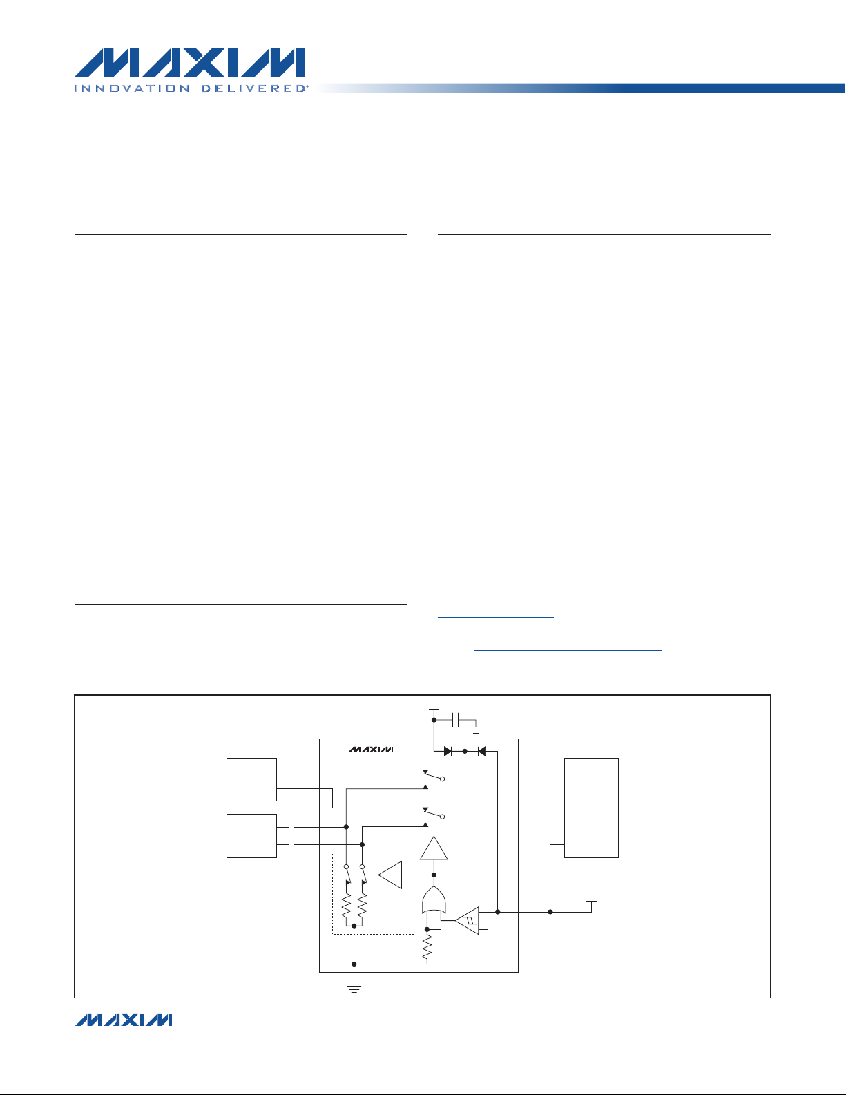
Typical Operating Circuit
BUS
Detection
Detection
CC
CC
3.0V
0.1µF
V
CC
MAX14585/MAX14585A
HI-SPEED
USB
TRANSCEIVER
AUDIO
AMPLIFIER
����������������������������������������������������������������� Maxim Integrated Products 1
UNC1
UNC2
AN01
AN02
GND
MAX14585
ONLY
AOR
V
CCINT
V
VBDET
COM1
COM2
V
B
COMBINATION
USB AND AUDIO
CONNECTOR
V
BUS
For pricing, delivery, and ordering information, please contact Maxim Direct at 1-888-629-4642,
or visit Maxim’s website at www.maxim-ic.com.
Page 2
MAX14585/MAX14585A
Hi-Speed USB and Audio Switches with Negative Signal
Capability and High-Voltage-Tolerable V
BUS
Detection
ABSOLUTE MAXIMUM RATINGS
(Voltages referenced to GND.)
VCC, AOR ................................................................-0.3V to +6V
VB ..........................................................................-0.3V to +30V
UNC_, ANO_, COM_ (VCC R 2.7V) ...-1.9V to min(VCC + 0.3V, 3.7V)
UNC_, COM_ (VB R 4.5V, VCC < 2.7V) ................-0.3V to +3.7V
UNC_, ANO_, COM_ (VCC < 2.7V) .. -0.3V to min(VCC + 0.3V, 3.7V)
UNC_, ANO_, COM_ (VCC = 0V, VB = 0V) .............-0.3V to +6V
Continuous Current into Any Pin ................................... Q100mA
Stresses beyond those listed under “Absolute Maximum Ratings” may cause permanent damage to the device. These are stress ratings only, and functional operation of the device at these or any other conditions beyond those indicated in the operational sections of the specifications is not implied. Exposure to absolute
maximum rating conditions for extended periods may affect device reliability.
Continuous Power Dissipation (TA = +70NC)
UTQFN (derate 7mW/NC above +70NC) ......................559mW
Operating Temperature Range .......................... -40NC to +85NC
Junction Temperature Range ........................... -40NC to +150NC
Storage Temperature Range ............................ -65NC to +150NC
Lead Temperature (soldering, 10s) ................................+300NC
Soldering Temperature (reflow) ......................................+260NC
PACKAGE THERMAL CHARACTERISTICS (Note 1)
UTQFN
Junction-to-Ambient Thermal Resistance (BJA) .....143.2NC/W
Junction-to-Case Thermal Resistance (BJC) ............20.1NC/W
Note 1: Package thermal resistances were obtained using the method described in JEDEC specification JESD51-7, using a four-
layer board. For detailed information on package thermal considerations, refer to www.maxim-ic.com/thermal-tutorial.
ELECTRICAL CHARACTERISTICS
(TA = -40NC to +85NC, unless otherwise noted. Typical values are at VCC = 3V, TA = +25NC.) (Note 2)
PARAMETER SYMBOL CONDITIONS MIN TYP MAX UNITS
POWER SUPPLY
Power-Supply Range V
Supply Current I
Power-Supply Rejection Ratio PSRR
VB Detect Threshold V
VB Detect Hysteresis V
VB Detect Leakage Current VB = 5.5V 40
ANALOG SWITCH
Analog-Signal Range
ANO_ On-Resistance R
UNC_ On-Resistance R
ANO_ On-Resistance Match
Between Channels
CC
SUPPLY
VBDET
VBDET_H
V
UNC_
V
ANO_
V
COM_
ON(NO)
ON(NC)
DR
ON(NO)
VCC = 4.2V, 0V < V
V
R 1.4V
AOR
f = 10kHz, VCC = 3.0 Q 0.3V,
R
= 50I
COM_
V
rising, VCC R 2.7V
BUS
V
falling, VCC R 2.7V
BUS
VCC R 2.7V for UNC_
,
VCC R 2.7V for ANO_, COM_
VCC = 3V, V
I
= 10mA
COM_
VCC = 3V, V
I
= 10mA
COM_
VB = 4.5V, VCC = 0V to 5.5V, V
to 2.5V, V
VCC = 3V, V
(Note 3)
AOR
AOR
= -1.5V, +1.5V
ANO_
= 0V to VCC,
UNC_
= 0V, I
= 0V, I
ANO_
< 0.4V,
COM_
COM_
UNC_
= 10mA
= 10mA
= 0V
2.7 5.5 V
7 14
100 dB
3 3.3 3.6 V
0.2 V
0
-1.8
min(3.6V,
VCC)
min(3.6V,
VCC)
3 6
3 6
3 6
0.2
FA
FA
V
I
I
I
����������������������������������������������������������������� Maxim Integrated Products 2
Page 3

MAX14585/MAX14585A
Hi-Speed USB and Audio Switches with Negative Signal
Capability and High-Voltage-Tolerable V
BUS
ELECTRICAL CHARACTERISTICS (continued)
(TA = -40NC to +85NC, unless otherwise noted. Typical values are at VCC = 3V, TA = +25NC.) (Note 2)
PARAMETER SYMBOL CONDITIONS MIN TYP MAX UNITS
UNC_ On-Resistance Match
Between Channels
ANO_ On-Resistance Flatness R
UNC_ On-Resistance Flatness R
DR
FLAT(NO)
FLAT(NC)
Shunt Switch Resistance R
AOR Pulldown Resistor R
UNC_ Off-Leakage Current I
ANO_ Off-Leakage Current I
COM_ Off-Leakage Current I
COM_ On-Leakage Current I
UNC_(OFF)
ANO_(OFF)
COM_(OFF)
COM_(ON)
Turn-On Time t
Turn-Off Time t
Break-Before-Make Time Delay t
Output Skew (Same Switch) t
Output Skew Between Switches t
ANO_ Off-Capacitance C
UNC_ Off-Capacitance C
NO_(OFF)VANO_
NC_(OFF)VUNC_
ON(NC)
SH
AOR
ON
OFF
D
SK(P)
SK(O)
VCC = 3V, V
UNC_
= 0V, I
COM_
= 10mA
(Note 3)
VCC = 3V, I
COM_
= 10mA, V
ANO_
= -1.5V
to +1.5V (Note 4)
VCC = 3V, I
COM_
= 10mA, V
UNC_
= 0V to
VCC (Note 4)
I
ANO_
= 2mA, V
CC
R 2.7V
250 1200
Switch open, V
V
= -1.5V, 2.5V, VCC = 3V
COM_
MAX14585A, switch open, V
0V, V
V
CC
V
UNC_
= 0V, 2.5V, VCC = 3V
COM_
= 0V, V
COM_
= V
ANO_
USB mode
Audio mode
ANO_ to COM_,
Figure 1
UNC_ to COM_,
Figure 1
ANO_ from
COM_,
Figure 1
UNC_ from
COM_,
Figure 1
= 2.5V, 0V
UNC_
ANO_
= 3.6V,
= unconnected
V
= 3V, V
CC
ANO_
2.5V, unconnected,
V
= 0V, 2.5V
COM_
V
= 3V, V
CC
UNC_
2.5V, unconnected,
V
= -1.5V, 2.5V
COM_
V
= 3V, V
CC
RL = 50I; V
ANO_
AOR
VB = 0V to 5V or VB = 5V,
V
= 0V to V
AOR
V
= 3V, V
CC
RL = 50I; V
UNC_
AOR
VB = 0V to 5V
V
= 3V, V
CC
RL = 50I; V
ANO_
AOR
VB = 0V to 5V
V
= 3V, V
CC
RL = 50I; V
UNC_
AOR
VB = 0V to 5V or VB = 5V,
V
= 0V to V
AOR
= 2.5V,
= 0V,
= 0V,
= 1.5V,
= 0V,
CC
= 1.5V,
= 0V,
= 1.5V,
= 0V,
= 1.5V,
= 0V,
CC
-100 +100 nA
-100 +100 nA
-10 +800
-200 +200 nA
-200 +200 nA
RL = 50I, time delay between one side of
the switch open and the other side closed
Figure 2 40 ps
Figure 2 40 ps
= 0.5V
= 0.5V
, DC bias = 0V, f = 1MHz 2.5 pF
P-P
, DC bias = 0V, f = 1MHz 2.5 pF
P-P
Detection
0.2
0.04 0.2
0.04 0.2
700 1300
45 120
45 120
8 40
8 40
28
I
I
I
I
kI
FA
Fs
Fs
Fs
Fs
Fs
����������������������������������������������������������������� Maxim Integrated Products 3
Page 4
MAX14585/MAX14585A
Hi-Speed USB and Audio Switches with Negative Signal
Capability and High-Voltage-Tolerable V
BUS
Detection
ELECTRICAL CHARACTERISTICS (continued)
(TA = -40NC to +85NC, unless otherwise noted. Typical values are at VCC = 3V, TA = +25NC.) (Note 2)
PARAMETER SYMBOL CONDITIONS MIN TYP MAX UNITS
V
= 0.5V
On-Capacitance C
COM_(ON)
COM_
f = 240MHz, RL = 50I
AC PERFORMANCE
ANO_ -3dB Bandwidth BW
UNC_ -3dB Bandwidth BW
Off-Isolation
Crosstalk
Total Harmonic Distortion Plus
Noise
THD+N
RS = RL = 50I, V
NO
RS = RL = 50I, V
NC
f = 100kHz, V
Figure 3
f = 100kHz, V
Figure 3 (Note 5)
ANO_ to COM_, f = 20Hz to 20kHz,
V
= 0.5V
COM_
LOGIC INPUT
AOR Input Logic-High V
AOR Input Logic-Low V
AOR Input Leakage Current I
IH
IN
IL
VCC R 2.7V
VCC R 2.7V
V
= 0V or VCC, VCC R 2.7V
AOR
ESD PROTECTION
Human Body Model
COM1, COM2
IEC 61000-4-2 Air Gap Discharge
IEC 61000-4-2 Contact Discharge
All Other Pins Human Body Model
Note 2: All devices are 100% production tested at TA = +25NC. Limits over the operating temperature range are guaranteed by
design; not production tested.
Note 3: DR
ON(MAX)
= ABS(R
ON(CH1)
- R
ON(CH2)
).
Note 4: Flatness is defined as the difference between the maximum and minimum value of on-resistance, as measured over speci-
fied analog-signal ranges.
Note 5: Between two switches.
, DC bias = 0V,
P-P
= 0dBm, Figure 3
ANO_
= 0dBm, Figure 3
UNC_
= 1V
COM_
= 1V
COM_
, DC bias = 0V, RL = 600I
P-P
, RL = 50I,
RMS
, RL = 50I,
RMS
6.7 pF
960 MHz
960 MHz
-84 dB
-86 dB
0.042 %
1.4 V
0.4 V
-22 +22
Q15
Q8
Q8
Q2
FA
kV
kV
V
IN_
LOGIC
INPUT
CL INCLUDES FIXTURE AND STRAY CAPACITANCE.
V
RL + R
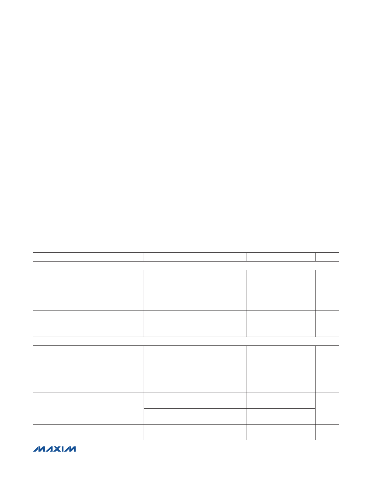
Figure 1. Switching Time
����������������������������������������������������������������� Maxim Integrated Products 4
ANO_
OR UNC_
CONTROL
= V
OUT
MAX14585
MAX14585A
R
IN_ (
L
ON
COM_
)
V
LOGIC
INPUT
V
OUT
R
L
C
L
SWITCH
OUTPUT
IH
V
IL
0V
50%
V
OUT
0.9 x V
0UT
t
ON
CONTROL DEPENDS ON SWITCH CONFIGURATION;
INPUT POLARITY DETERMINED BY SENSE OF SWITCH.
tR < 5n s
t
< 5n s
F
t
OFF
0.1 x V
OUT
Page 5

MAX14585/MAX14585A
Hi-Speed USB and Audio Switches with Negative Signal
Capability and High-Voltage-Tolerable V
MAX14585
50%
50%
50%
MAX14585A
CONTROL
VIL TO V
t
PHLX
COM1
COM2
IH
50%
50%
50%
t
= t
PLH
V
OUT+
t
= t
PHL
t
R
L
R
L
SK(O)
t
SK(P)
CONTROL DEPENDS ON SWITCH CONFIGURATION.
V
OUT-
t
INRISE
90%
10% 10%
t
OUTRISE
10% 10%
= |t
= |t
90%
PLHX
PHLX
PLHX
PLHX
OR t
OR t
PLHY
PHLY
- t
PLHY
- t
PHLX
UNC1 OR
R
S
V
IN+
V
IN-
V
CC
V
IN+
0V
V
CC
V
IN-
0V
V
CC
V
OUT+
0V
ANO1
UNC2 OR
R
S
ANO2
t
PLHX
BUS
| OR |t
PHLX
| OR |t
PLHY
t
INFALL
90%
90%
Detection
- t
|
PHLY
- t
|
PHLY
t
OUTFALL
V
CC
V
OUT-
0V
t
PHLY
50%
Figure 2. Output Skew
COM1
MAX14585
UNC1
MAX14585A
50
Ω
ANO1*
OFF-ISOLATION IS MEASURED BETWEEN COM_ AND "OFF" ANO_ OR UNC_ TERMINAL ON EACH SWITCH.
ON-LOSS IS MEASURED BETWEEN COM_ AND "ON" ANO_ OR UNC_ TERMINAL ON EACH SWITCH.
CROSSTALK IS MEASURED FROM ONE CHANNEL TO THE OTHER CHANNEL.
Figure 3. On-Loss, Off-Isolation, and Crosstalk
����������������������������������������������������������������� Maxim Integrated Products 5
50%
t
PLHY
V
NETWORK
ANALYZER
Ω
V
IN
50
50Ω
OFF-ISOLATION = 20log
ON-LOSS = 20log
V
OUT
MEAS REF
50
Ω
50
Ω
CROSSTALK = 20log
OUT
V
IN
V
OUT
V
IN
V
OUT
V
IN
*FOR CROSSTALK THIS PIN IS ANO2.
UNC2 AND COM2 ARE OPEN.
Page 6
MAX14585/MAX14585A
Hi-Speed USB and Audio Switches with Negative Signal
Capability and High-Voltage-Tolerable V
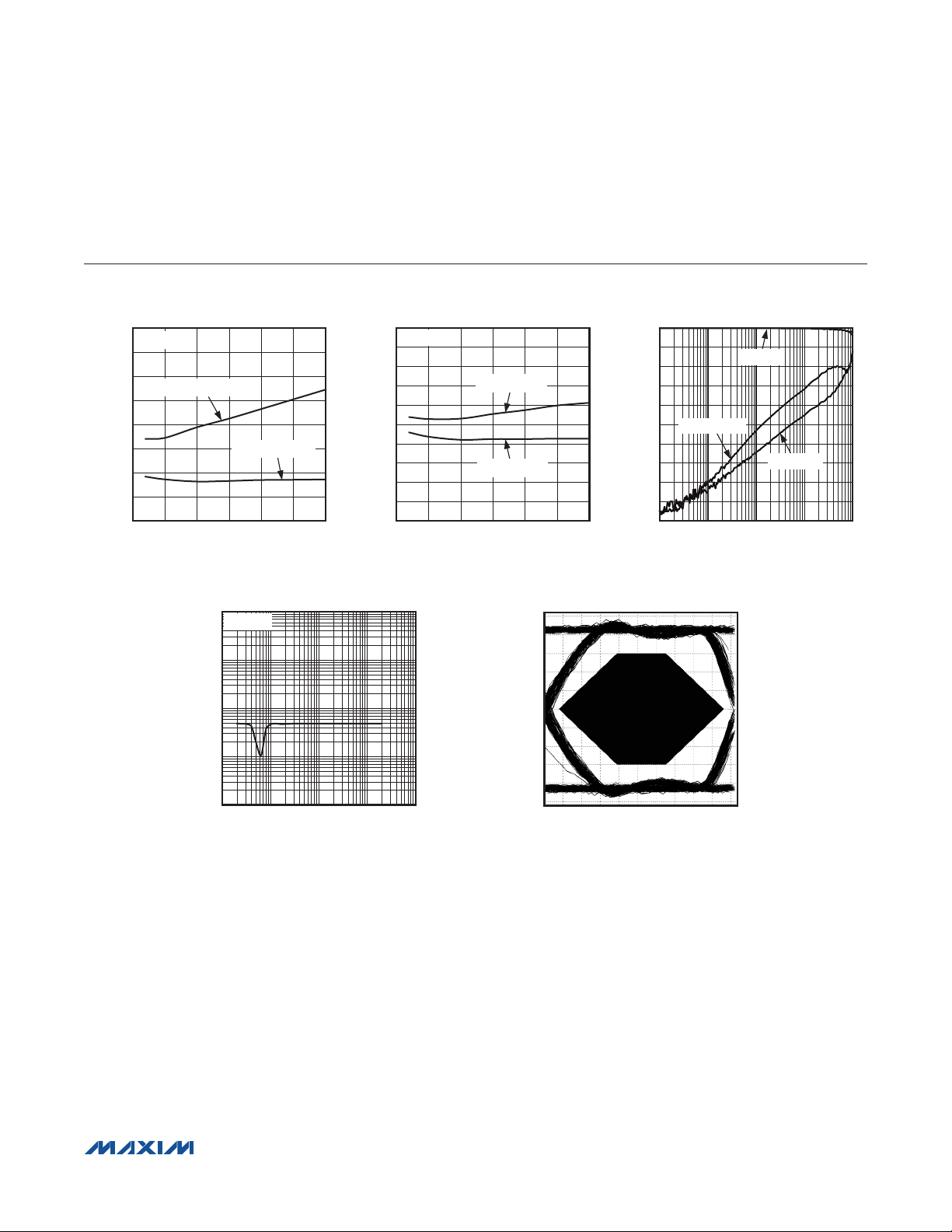
Typical Operating Characteristics
(VCC = 3.0V, TA = +25NC, unless otherwise noted.)
UNC_ ON-RESISTANCE vs. COM_ VOLTAGE
3.3
I
= 10mA
UNC_
3.2
3.1
3.0
2.9
2.8
ON-RESISTANCE (Ω)
2.7
2.6
2.5
0 4
V
COM_
VCC = 2.7V
= 5V
V
CC
(V)
ANO_ ON-RESISTANCE vs. COM_ VOLTAGE
4.0
3.8
3.6
3.4
3.2
3.0
2.8
ON-RESISTANCE (Ω)
2.6
2.4
2.2
2.0
-2 3
TA = +85°C
V
COM_
TA = +25°C
TA = -40°C
(V)
VCC = 3V
I
ANO_
MAX14585/85A toc01
321
MAX14585/85A toc04
= 10mA
210-1
ANO_ ON-RESISTANCE vs. COM_ VOLTAGE
3.3
I
= 10mA
ANO_
3.2
3.1
3.0
2.9
2.8
ON-RESISTANCE (Ω)
2.7
2.6
2.5
-2 4
V
CC
V
= 5V
COM_
VCC = 2.7V
(V)
COM_ ON-LEAKAGE CURRENT
vs. TEMPERATURE
40
V
= 2.5V
COM_
35
30
25
20
15
10
ON-LEAKAGE CURRENT (nA)
5
0
-40 85
TEMPERATURE (°C)
4.0
3.8
3.6
MAX14585/85A toc02
3.4
3.2
3.0
2.8
ON-RESISTANCE (Ω)
2.6
2.4
2.2
32-1 0 1
6035-15 10
2.0
600
500
MAX14585/85A toc05
400
300
200
OFF-LEAKAGE CURRENT (µA)
100
0
BUS
Detection
UNC_ ON-RESISTANCE vs. COM_ VOLTAGE
TA = +85°C
0 3.0
V
COM_
TA = +25°C
TA = -40°C
(V)
VCC = 3V
= 10mA
I
UNC_
2.52.01.51.00.5
COM_ OFF-LEAKAGE CURRENT
vs. TEMPERATURE
VCC = 0V
= 3.6V
V
COM_
-40 85
TEMPERATURE (°C)
603510-15
MAX14585/85A toc03
MAX14585/85A toc06
SUPPLY CURRENT vs. SUPPLY VOLTAGE
10
9
8
7
6
5
4
3
SUPPLY CURRENT (µA)
2
1
0
TA = -40°C
2.5 5.5
SUPPLY VOLTAGE (V)
TA = +25°C
����������������������������������������������������������������� Maxim Integrated Products 6
TA = +85°C
5.04.54.03.53.0
MAX14585/85A toc07
CURRENT (µA)
B
V
VB SUPPLY CURRENT vs. SUPPLY VOLTAGE
70
V
= 0V OR 3V
AOR
60
50
40
30
20
10
0
0 30
VB VOLTAGE (V)
252015105
MAX14585/85A toc08
THRESHOLD (V)
B
V
VB DETECT THRESHOLD vs. TEMPERATURE
3.5
3.4
3.3
3.2
3.1
3.0
2.9
2.8
2.7
2.6
2.5
-40 85
VB RISING
VB FALLING
603510-15
TEMPERATURE (°C)
MAX14585/85A toc09
Page 7
MAX14585/MAX14585A
Hi-Speed USB and Audio Switches with Negative Signal
Capability and High-Voltage-Tolerable V
Typical Operating Characteristics (continued)
(VCC = 3.0V, TA = +25NC, unless otherwise noted.)
TURN-OFF TIME vs. SUPPLY VOLTAGE
40
TOGGLE V
35
30
25
20
15
TURN-ON TIME (µs)
10
5
0
2.5 5.5
B
ANO_ FROM COM_
UNC_ FROM COM_
SUPPLY VOLTAGE (V)
TOTAL HARMONIC DISTORTION PLUS NOISE
10
RL = 600Ω
1
0.1
THD+N (%)
0.01
0.001
10 100,000
MAX14585/85A toc10
5.04.53.0 3.5 4.0
vs. FREQUENCY
10,0001000100
FREQUENCY (Hz)
TURN-ON TIME vs. SUPPLY VOLTAGE
100
TOGGLE V
90
80
70
60
50
40
TURN-ON TIME (µs)
30
20
10
0
2.5 5.5
B
SUPPLY VOLTAGE (V)
MAX14585/85A toc13
UNC_ TO COM_
ANO_ TO COM_
0.5
0.4
0.3
0.2
0.1
-0.1
-0.2
DIFFERENTIAL SIGNAL (V)
-0.3
-0.4
-0.5
0
-10
-20
MAX14585/85A toc11
-30
-40
-50
-60
MAGNITUDE (dB)
-70
-80
-90
5.04.54.03.53.0
-100
UNC_ EYE DIAGRAM
0
TIME ((x10-9)s)
BUS
Detection
FREQUENCY RESPONSE
ON-LOSS
OFF-ISOLATION
CROSSTALK
0.1 1000
FREQUENCY (MHz)
MAX14585/85A toc14
2.00 0.2 0.4 0.6 0.8 1.0 1.2 1.4 1.6 1.8
100101
MAX14585/85A toc12
����������������������������������������������������������������� Maxim Integrated Products 7
Page 8
MAX14585/MAX14585A
Hi-Speed USB and Audio Switches with Negative Signal
Capability and High-Voltage-Tolerable V
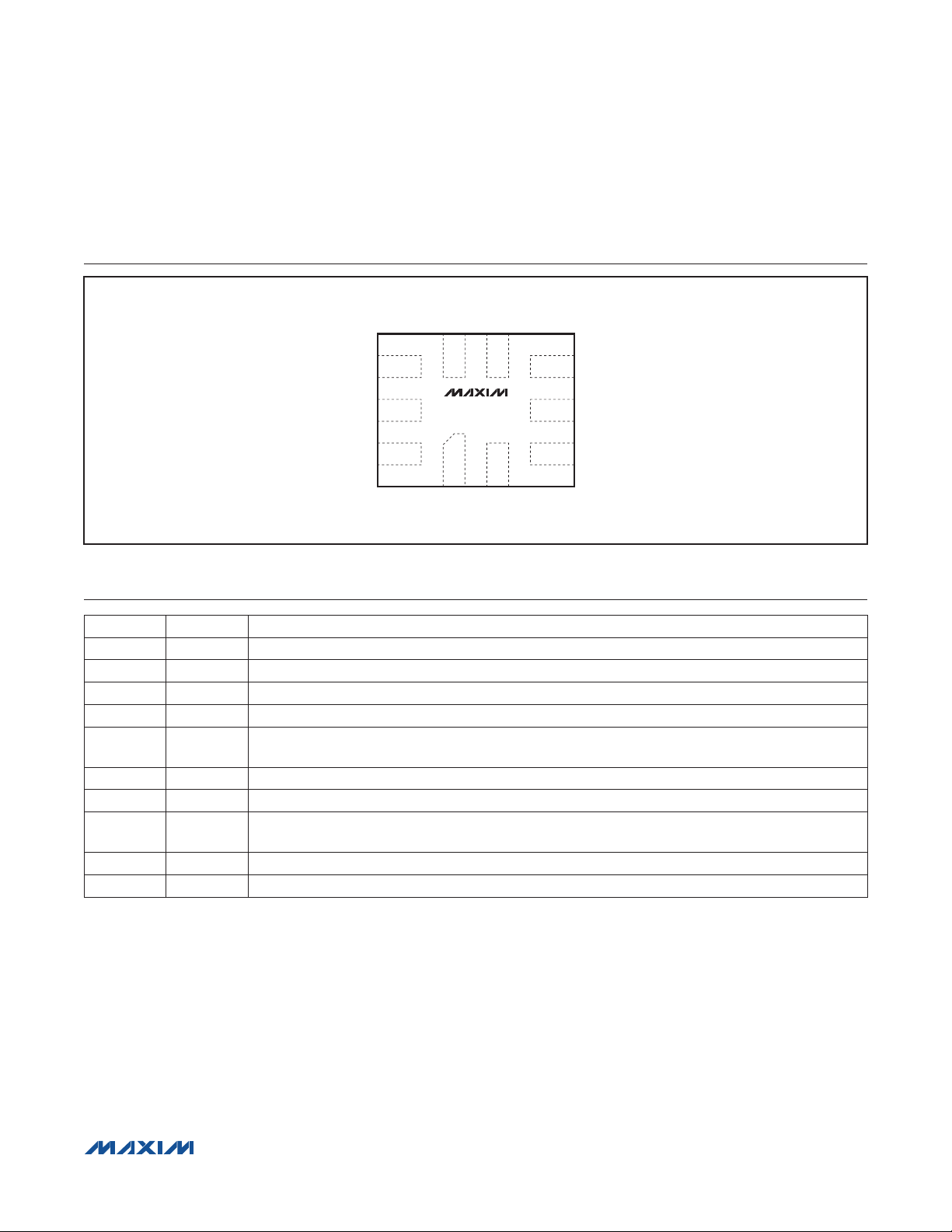
TOP VIEW
COM2 COM1
AOR
8
9
V
B
10
UNC2
+
PIN NAME FUNCTION
1 UNC1 USB Input 1. Normally closed terminal for switch 1.
2 ANO2 Audio Input 2. Normally open terminal for switch 2.
3 ANO1 Audio Input 1. Normally open terminal for switch 1.
4 GND Ground
5 V
6 COM1 Common Terminal for Switch 1
7 COM2 Common Terminal for Switch 2
8 AOR
9 V
10 UNC2 USB Input 2. Normally closed terminal for switch 2.
CC
Positive Supply-Voltage Input. Bypass VCC to GND with a 0.1FF capacitor as close as possible to the
device.
Audio Override Input. Drive AOR low to have VB control the switch. Drive AOR high to connect COM_
to ANO_. AOR has an internal pulldown resistor to GND.
V
B
Detection Input. If VB R V
BUS
7 6
MAX14585
MAX14585A
1 2
UNC1 ANO2
UTQFN
, COM_ connects to UNC_. Otherwise, COM_ connects to ANO_.
VBDET
5
V
CC
4
GND
3
ANO1
BUS
Detection
Pin Configuration
Pin Description
����������������������������������������������������������������� Maxim Integrated Products 8
Page 9
MAX14585/MAX14585A
Hi-Speed USB and Audio Switches with Negative Signal
Capability and High-Voltage-Tolerable V
Functional Diagrams/Truth Table
V
CC
UNC1
UNC2
ANO1
ANO2
MAX14585
V
CCINT
V
VBDET
COM1
COM2
V
B
UNC1
UNC2
ANO1
ANO2
MAX14585A
BUS
V
CC
V
Detection
CCINT
COM1
COM2
V
B
V
VBDET
GND
AOR
> V
< V
X = DON’T CARE
V
B
VBDET
VBDET
X
MAX14585/MAX14585A
AOR
0
0
1
Detailed Description
The MAX14585/MAX14585A are high-ESD-protected
single DPDT switches that operate from a 2.7V to 5.5V
supply and are designed to multiplex Hi-Speed USB
signals and AC-coupled analog signals. These switches
combine the low on-capacitance (CON) and low on-resistance (RON) necessary for high-performance switching
applications. These devices meet the requirements for
USB low-speed and full-speed signaling. The negative
signal capability of the analog channel allows signals
below ground to pass through without distortion.
UNC_
ON
OFF
OFF
ANO_
OFF
ON
ON
GND
MAX14585
ANO_SHUNT
ON
OFF
OFF
AOR
Analog-Signal Levels
The devices are bidirectional, allowing ANO_, UNC_, and
COM_ to be configured as either inputs or outputs. Note
that UNC_ and ANO_ are only protected against ESD up
to Q2kV (HBM) and could require additional ESD protection if used as outputs. These devices feature a charge
pump that generates a negative supply to allow analog
signals as low as -1.8V to pass through ANO_ when VCC
supply is greater than 2.7V. This allows AC-coupled signals that drop below ground to pass when operating from
a single power supply.
����������������������������������������������������������������� Maxim Integrated Products 9
Page 10
MAX14585/MAX14585A
Hi-Speed USB and Audio Switches with Negative Signal
Capability and High-Voltage-Tolerable V
When VCC is below 2.7V and VB is less than 4.5V, the
switches accept signals from 0 to 3.6V but do not switch
according to the Functional Diagrams/Truth Table.
V
Detection Input
The devices feature a V
BUS
nects COM_ to UNC_ when VB exceeds the V
threshold (V
). For applications where V
VBDET
BUS
detection input (VB) that con-
detection
BUS
is always
BUS
present, drive the audio override input (AOR) high to connect ANO_ to COM_ (see the Functional Diagrams/Truth
Table). Drive AOR low to have VB control the switch posi-
tion. Drive AOR rail-to-rail to minimize power consumption.
The VB input is capable of handling voltage up to 28V
for higher V
application. In the case where the main
BUS
power VCC is lost due to an event such as a dead battery,
VB becomes the power supply if VB is greater than 4.5V.
Click-and-Pop Suppression (MAX14585)
The switched 700I (typ) shunt resistors on the MAX14585
automatically discharge any capacitance at the ANO_
terminals when they are unconnected from COM_. This
reduces audio click-and-pop sounds that can occur
when switching between USB and audio sources.
ESD protection structures are incorporated on all pins
to protect against electrostatic discharges up to Q2kV
(HBM) encountered during handling and assembly.
COM1 and COM2 are further protected against ESD up
to Q15kV (HBM) without damage. The ESD structures
withstand high ESD in both normal operation and
when the devices are powered down. After an ESD
event, the devices continue to function without latchup.
ESD performance depends on a variety of conditions.
Contact Maxim for a reliability report that documents test
setup, test methodology, and test results.
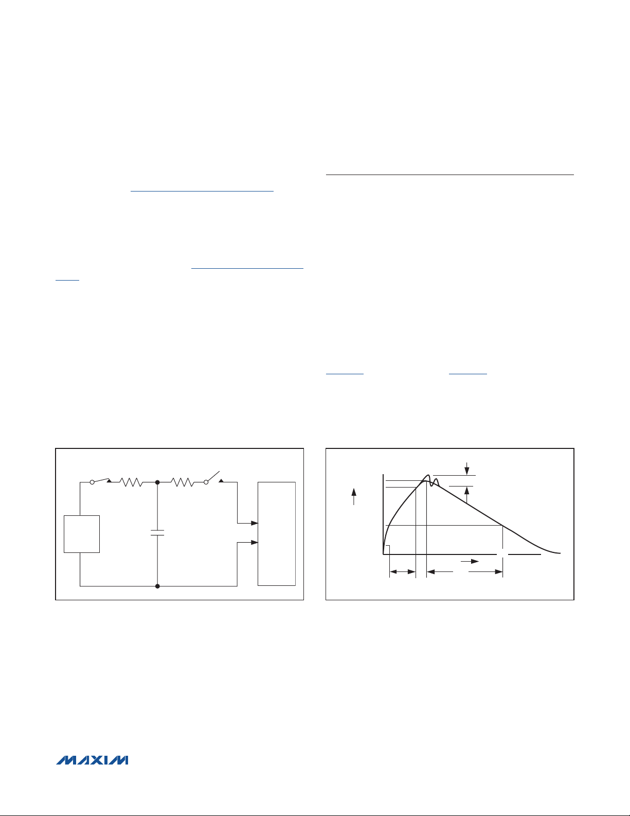
Figure 4 shows the HBM. Figure 5 shows the current
waveform it generates when discharged into a lowimpedance state. This model consists of a 100pF capacitor charged to the ESD voltage of interest that is then
discharged into the device through a 1.5kI resistor.
Applications Information
BUS
Detection
Extended ESD Protection
ESD Test Conditions
Human Body Model
R
C
Ω
1M
CHARGE-CURRENT-
LIMIT RESISTOR
HIGH-
VOLTAGE
DC
SOURCE
Figure 4. Human Body ESD Test Model
C
s
100pF
���������������������������������������������������������������� Maxim Integrated Products 10
R
D
1500Ω
DISCHARGE
RESISTANCE
STORAGE
CAPACITOR
DEVICE
UNDER
TEST
IP 100%
90%
AMPERES
36.8%
10%
0
0
t
RL
Figure 5. Human Body Current Waveform
I
r
TIME
t
DL
CURRENT WAVEFORM
PEAK-TO-PEAK RINGING
(NOT DRAWN TO SCALE)
Page 11

MAX14585/MAX14585A
Hi-Speed USB and Audio Switches with Negative Signal
Capability and High-Voltage-Tolerable V
R
C
50MΩ TO 100MΩ
CHARGE CURRENT
LIMIT RESISTOR
HIGH-
VOLTAGE
DC
SOURCE
Figure 6. IEC 61000-4-2 ESD Test Model
100%
90%
PEA K
I
C
s
150pF
I
R
D
330Ω
DISCHARGE
RESISTANCE
STORAGE
CAPACITOR
DEVICE
UNDER
TEST
The IEC 61000-4-2 standard covers ESD testing and
performance of finished equipment. It does not specifically refer to integrated circuits. The major difference
between tests done using the HBM and IEC 61000-4-2
is higher peak current in IEC 61000-4-2, because series
resistance is lower in the IEC 61000-4-2 model. Hence,
the ESD withstand voltage measured to IEC 61000-4-2
is generally lower than that measured using the HBM.
Figure 6 shows the IEC 61000-4-2 model and Figure 7
shows the current waveform for the Q8kV, IEC 61000-4-2,
Level 4, ESD Contact-Discharge Method.
Hi-Speed USB requires careful PCB layout with 45I
single-ended/90I differential controlled-impedance
matched traces of equal lengths. Ensure that bypass
capacitors are as close to the device as possible. Use
large ground planes where possible.
Ordering Information/
BUS
Detection
IEC 61000-4-2
Layout
Selector Guide
10%
tr = 0.7ns to 1ns
Figure 7. IEC 61000-4-2 ESD Generator Current Waveform
30ns
60ns
Chip Information
PROCESS: BiCMOS
PART
MAX14585EVB+T AAY Yes 10 UTQFN
t
MAX14585AEVB+T AAZ No 10 UTQFN
Note: All devices are specified over the -40°C to +85°C temperature range.
+Denotes a lead(Pb)-free/RoHS-compliant package.
T = Tape and reel.
TOP
MARK
SHUNT
RESISTOR
PINPACKAGE
Package Information
For the latest package outline information and land patterns
(footprints), go to www.maxim-ic.com/packages. Note that a
“+”, “#”, or “-” in the package code indicates RoHS status only.
Package drawings may show a different suffix character, but
the drawing pertains to the package regardless of RoHS status.
PACKAGE
TYPE
10 UTQFN V101A1CN+1
PACKAGE
CODE
OUTLINE
NO.
21-0028 90-0287
LAND
PATTERN NO.
���������������������������������������������������������������� Maxim Integrated Products 11
Page 12

MAX14585/MAX14585A
Hi-Speed USB and Audio Switches with Negative Signal
Capability and High-Voltage-Tolerable V
BUS
Detection
Revision History
REVISION
NUMBER
0 5/11 Initial release —
REVISION
DATE
DESCRIPTION
PAGES
CHANGED
Maxim cannot assume responsibility for use of any circuitry other than circuitry entirely embodied in a Maxim product. No circuit patent licenses are implied.
Maxim reserves the right to change the circuitry and specifications without notice at any time.
Maxim Integrated Products, 120 San Gabriel Drive, Sunnyvale, CA 94086 408-737-7600 12
©
2011 Maxim Integrated Products Maxim is a registered trademark of Maxim Integrated Products, Inc.
 Loading...