

Page 1
19-5248; Rev 0; 4/10
EVALUATION KIT
AVAILABLE
100Mbps, 16-Channel LLTs
General Description
The MAX14548E/MAX14548AE 16-channel, bidirectional
level translators (LLTs) provide the level shifting necessary for 100Mbps data transfer in multivoltage systems.
Externally applied voltages, VCC and VL, set the logic
levels on either side of the device. Logic signals present
on the VL side of the device appear as a high-voltage
logic signal on the VCC side of the device and vice versa.
The devices feature a programming frequency input (PF)
that adjusts the one-shot accelerator on-time to guarantee a bit rate of 100Mbps with a load capacitance < 15pF
and VL > 1.1V (MAX14548E) or VL > 1.4V (MAX14548AE)
when driven low. The MAX14548E can drive capacitive
loads up to 50pF with a guaranteed bit rate of 40Mbps
when VL R 1.1V and PF is driven high. The MAX14548AE
can drive capacitive loads up to 50pF with a guaranteed
bit rate of 40Mbps when VL R 1.1V and PF is driven high.
The device operate at full speed with external drivers
that source as low as 4mA output current. Each I/O channel is pulled up to VCC or VL by an internal 35FA current
source, allowing both devices to be driven by either
push-pull or open-drain drivers.
The devices feature multiple power-saving features
including an enable input (EN) that places the device
into a low-power shutdown mode when driven low and
an automatic shutdown mode that disables the part
when VCC is less than VL. The MAX14548AE output driver is designed to operate at full speed (100Mbps) with
VL > 1.4V, which reduces the dynamic supply current vs.
the MAX14548E. The state of I/O V
high-impedance state during shutdown.
The devices operate with VCC voltages from +1.7V to
+3.6V and VL voltages from +1.1V to +3.6V, making
them ideal for data transfer between low-voltage ASICs/
PLDs and higher voltage systems. The devices are available in a 40-bump WLP (2.16mm x 3.46mm) package
with 0.4mm ball pitch, and operate over the extended
-40NC to +85NC temperature range.
and I/O VL_are in
CC_
Features
S Bidirectional Level Translation
S 100Mbps Guaranteed Data Rate
S +1.7V to +3.6V Supply Voltage Range for V
S +1.1V to +3.6V Supply Voltage Range for V
(VCC > VL)
S -40NC to +85NC Extended Operating Temperature
Range
CC
L
Applications
CMOS Logic-Level Translation
Low-Voltage ASIC Level Translation
Smart Card Readers
Portable Communication Devices
Cell Phones
GPS
Telecommunications Equipment
Typical Operating Circuit appears at end of data sheet.
MAX14548E/MAX14548AE
Ordering Information/Selector Guide
PART
MAX14548EEWL+ 40 WLP 100 40 —
MAX14548AEEWL+ 40 WLP 100 40 Yes (VL > 1.1V)
Note: All devices operate over the -40°C to +85°C operating temperature range.
+Denotes a lead(Pb)-free/RoHS-compliant package.
_______________________________________________________________ Maxim Integrated Products 1
PIN-
PACKAGE
BIT RATE (PF = LOW)
LOAD CAPACITANCE < 15pF
(Mbps)
For pricing, delivery, and ordering information, please contact Maxim Direct at 1-888-629-4642,
or visit Maxim’s website at www.maxim-ic.com.
BIT RATE (PF = HIGH)
LOAD CAPACITANCE < 50pF
(Mbps)
LOW DYNAMIC
SUPPLY
CURRENT
Page 2
100Mbps, 16-Channel LLTs
ABSOLUTE MAXIMUM RATINGS
(All voltages referenced to GND.)
VCC, VL, EN, PF....................................................... -0.3V to +4V
I/O V
................................................... -0.3V to (VCC + 0.3V)
CC_
I/O VL_ ......................................................... -0.3V to (VL + 0.3V)
Short-Circuit Duration I/O VL_,
I/O V
to GND ....................................................Continuous
CC_
Continuous Power Dissipation (TA = +70NC)
40-Bump WLP (derate 17.2mW/NC above +70NC) ....1379mW
Note 1: Package thermal resistances were obtained using the method described in JEDEC specification JESD51-7, using a four-
layer board. For detailed information on package thermal considerations, refer to www.maxim-ic.com/thermal-tutorial.
Stresses beyond those listed under “Absolute Maximum Ratings” may cause permanent damage to the device. These are stress ratings only, and functional
operation of the device at these or any other conditions beyond those indicated in the operational sections of the specifications is not implied. Exposure to absolute
maximum rating conditions for extended periods may affect device reliability.
ELECTRICAL CHARACTERISTICS
(VCC = +1.7V to +3.6V, VL = +1.1V to +3.6V, VCC > VL, EN = VL, C
noted. Typical values are at VCC = +2.8V, VL = +1.8V and TA = +25NC.) (Notes 2, 3)
PARAMETER SYMBOL CONDITIONS MIN TYP MAX UNITS
POWER SUPPLIES
VL Supply Range V
MAX14548E/MAX14548AE
VCC Supply Range V
Supply Current from V
Supply Current from V
CC
L
VCC Shutdown Supply
Current
VL Shutdown Mode Supply
Current
Dynamic Supply Current I
I/O V
, I/O VL_ Three-State
CC_
Leakage Current
EN, PF Input Leakage Current I
VL Shutdown Threshold V
VL - VCC Shutdown Threshold
High
VL - VCC Shutdown Threshold
Low
I/O VL_ Pullup Current I
I/O V
I/O VL_ to I/O V
Pullup Current I
CC_
DC
CC_
Resistance
L
CC
I
QVCC
I
QVL
I
SHDN-VCC
I
SHDN-VL
D
I
LEAK
LEAK_EN_PF
TH_VL
V
TH_H
V
TH_L
VL_PU_
VCC_PU_
R
IOVL_IOVCC
I/O V
CC_
I/O V
CC_
TA = +25NC, EN = GND, unconnected
I/O pins
TA = +25NC, EN = GND, unconnected
I/O pins
TA = +25NC, EN = VL, VCC = GND,
unconnected I/O pins
One I/O switching at
25MHz; all other I/O
connected to VCC or
VL; C
LOAD
TA = +25NC, EN = GND
TA = +25NC
VCC rising (VL = 3.6V) (Note 4) 0.05 0.3 0.65 V
VCC falling (VL = 3.6V) (Note 4) 0.2 0.52 0.85 V
I/O VL_ = GND, I/O V
I/O V
CC_
(Note 5) 3
Junction-to-Ambient Thermal Resistance (BJA)
(Note 1) ........................................................................58NC/W
Operating Temperature Range .......................... -40NC to +85NC
Storage Temperature Range ............................ -65NC to +150NC
Junction Temperature .....................................................+150NC
Soldering Temperature (reflow) ......................................+260NC
= 1FF, CVL = 1FF, TA = -40NC to +85NC, unless otherwise
VCC
1.1 3.6 V
1.7 3.6 V
= VCC, I/O VL_ = V
= VCC, I/O VL_ = V
L
L
40
20
0.1 1
0.1 1
0.1 2
MAX14548E 2.9
= 0pF
MAX14548AE 2.6
0.1 6
0.3 V
= GND 10 125
CC_
= GND, I/O VL_ = GND 15 90
1
FA
FA
FA
FA
mA
FA
FA
FA
FA
kI
2
Page 3

100Mbps, 16-Channel LLTs
ELECTRICAL CHARACTERISTICS (continued)
(VCC = +1.7V to +3.6V, VL = +1.1V to +3.6V, VCC > VL, EN = VL, C
noted. Typical values are at VCC = +2.8V, VL = +1.8V and TA = +25NC.) (Notes 2, 3)
PARAMETER SYMBOL CONDITIONS MIN TYP MAX UNITS
ESD PROTECTION
Human Body
I/O V
CC_
, I/O V
L_
Model,
C
VCC
C
= 1FF
VL
= 1FF,
All Other Pins
LOGIC LEVELS
I/O VL_ Input-Voltage High
Threshold
I/O VL_ Input-Voltage Low
Threshold
I/O V
Input-Voltage High
CC_
Threshold
I/O V
Input-Voltage Low
CC_
Threshold
EN, PF Input-Voltage High
Threshold
EN, PF Input-Voltage Low
Threshold
I/O VL_ Output-Voltage High V
I/O VL_ Output-Voltage Low,
Drop to GND
I/O V
I/O V
Output-Voltage High V
CC_
Output-Voltage Low,
CC_
Drop to GND
V
V
V
V
V
V
IHL
ILL
IHC
ILC
V
IH
V
IL
OHL
OLL
OHC
OLC
(Note 6)
(Note 6) 0.15 V
(Note 6)
(Note 6) 0.2 V
1.1V < VL < 1.3V
VL = 1.8V
1.1V < VL < 1.3V 0.4
VL = 1.8V 0.4
I/O VL_ source current = 10FA
I/O VL_ sink current = 20FA,
I/O V
I/O V
I/O V
I/O V
< 0.05V
CC_
source current = 10FA
CC_
sink current = 20FA,
CC_
< 0.05V
L_
RISE/FALL TIME ACCELERATOR STAGE
PF = low
Accelerator Pulse Duration
PF = high
VL Output Accelerator Source
Impedance
VCC Output Accelerator
Source Impedance
VL Output Accelerator Sink
Impedance
VCC Output Accelerator Sink
Impedance
VL = 1.62V 7
VL = 3.2V 4.43
VCC = 2.2V 14.2
VCC = 3.6V 11.2
VL = 1.62V 15.3
VL = 3.2V 15.3
VCC = 2.2V 20.3
VCC = 3.6V 19.5
= 1FF, CVL = 1FF, TA = -40NC to +85NC, unless otherwise
VCC
Unpowered
device
Powered device
On rising edge 2.65
On falling edge 2.5
On rising edge 4
On falling edge 3.7
VL -
0.2
VCC -
0.4
VL -
0.25
VL -
0.4
4/5 x
V
4/5 x
V
CC
MAX14548E/MAX14548AE
Q12
kV
Q5
Q2
L
1/3 x
V
L
1/3 x
V
CC
kV
V
V
V
V
V
V
V
V
ns
ns
I
I
I
I
3
Page 4
100Mbps, 16-Channel LLTs
HIGH-SPEED TIMING CHARACTERISTICS—MAX14548E
(VCC = +1.7V to +3.6V, VL = +1.1V to +3.6V, VCC > VL, EN = VL, PF = low, C
TA = -40NC to +85NC, unless otherwise noted. Typical values are at VCC = +2.8V, VL = +1.8V and TA = +25NC.) (Notes 2, 3)
PARAMETER SYMBOL CONDITIONS MIN TYP MAX UNITS
I/O V
I/O V
I/O VL_ Rise Time t
I/O VL_ Fall Time t
Propagation Delay
(Driving I/O VL_)
Propagation Delay
(Driving I/O V
Channel-to-Channel Skew t
Propagation Delay from
I/O VL_ to I/O V
Propagation Delay from
I/O V
Maximum Data Rate
MAX14548E/MAX14548AE
HIGH-SPEED TIMING CHARACTERISTICS—MAX14548AE
Rise Time t
CC_
Fall Time t
CC_
)
CC_
After EN
CC_
to I/O VL_ After EN
CC_
RVCC
FVCC
RVL
FVL
t
PVL-VCC
t
PVCC-VL
SKEW
t
EN-VCC
t
EN-VL
Input rise time < 2ns, Figure 1 2 ns
Input fall time < 2ns, Figure 1 2 ns
Input rise time < 2ns, Figure 2 2 ns
Input fall time < 2ns, Figure 2 2 ns
Input rise time < 2ns, Figure 1 2.75 ns
Input rise time < 2ns, Figure 2 2.26 ns
Input rise time/fall time < 2ns 0.2 ns
R
= 1MI, Figure 3
LOAD
R
= 1MI, Figure 3
LOAD
Push-pull operation 100
Open-drain operation 0.3
(VCC = +1.7V to +3.6V, VL = +1.4V to +3.6V, VCC > VL, EN = VL, PF = low, C
TA = -40NC to +85NC, unless otherwise noted. Typical values are at VCC = +2.8V, VL = +1.8V and TA = +25NC.) (Notes 2, 3)
PARAMETER SYMBOL CONDITIONS MIN TYP MAX UNITS
I/O V
I/O V
I/O VL_ Rise Time t
I/O VL_ Fall Time t
Propagation Delay
(Driving I/O VL_)
Propagation Delay
(Driving I/O V
Channel-to-Channel Skew t
Propagation Delay from
I/O VL_ to I/O V
Propagation Delay from
I/O V
Maximum Data Rate
Rise Time t
CC_
Fall Time t
CC_
)
CC_
After EN
CC_
to I/O VL_ After EN
CC_
RVCC
FVCC
RVL
FVL
t
PVL-VCC
t
PVCC-VL
SKEW
t
EN-VCC
t
EN-VL
Input rise time < 2ns, Figure 1 2 ns
Input fall time < 2ns, Figure 1 2 ns
Input rise time < 2ns, Figure 2 2 ns
Input rise time < 2ns, Figure 2 2 ns
Input rise time < 2ns, Figure 1 2.75 ns
Input rise time < 2ns, Figure 2 2.26 ns
Input rise time/fall time < 2ns 0.2 ns
R
= 1MI, Figure 3
LOAD
R
= 1MI, Figure 3
LOAD
Push-pull operation 100
Open-drain operation 0.3
= 1FF, CVL = 1FF, C
VCC
= 1FF, CVL = 1FF, C
VCC
IOVL
27
0.05
IOVL
27
0.05
P 15pF, C
P 15pF, C
IOVCC
IOVCC
P 15pF,
Fs
Fs
Mbps
P 15pF,
Fs
Fs
Mbps
4
Page 5
100Mbps, 16-Channel LLTs
LOW-SPEED TIMING CHARACTERISTICS—MAX14548E
(VCC = +1.7V to +3.6V, VL = +1.1V to +3.6V, VCC > VL, EN = VL, PF = high, C
TA = -40NC to +85NC, unless otherwise noted. Typical values are at VCC = +2.8V, VL = +1.8V and TA = +25NC.) (Notes 2, 3)
PARAMETER SYMBOL CONDITIONS MIN TYP MAX UNITS
I/O V
I/O V
I/O VL_ Rise Time t
I/O VL_ Fall Time t
Propagation Delay
(Driving I/O VL_)
Propagation Delay
(Driving I/O V
Channel-to-Channel Skew t
Propagation Delay from
I/O V
Propagation Delay from
I/O V
Maximum Data Rate
Rise Time t
CC_
Fall Time t
CC_
)
CC_
to I/O V
L_
to I/O VL_ After EN
CC_
CC_
After EN
RVCC
FVCC
RVL
FVL
t
PVL-VCC
t
PVCC-VL
SKEW
t
EN-VCC
t
EN-VL
Input rise time < 6ns, Figure 1 6 ns
Input fall time < 6ns, Figure 1 6 ns
Input rise time < 6ns, Figure 2 6 ns
Input rise time < 6ns, Figure 2 6 ns
Input rise time < 6ns, Figure 1 4 ns
Input rise time < 6ns, Figure 2 3.37 ns
Input rise time/fall time < 6ns 0.2 0.5 ns
R
= 1MI, Figure 3
LOAD
R
= 1MI, Figure 3
LOAD
Push-pull operation 40
Open-drain operation 0.3
LOW-SPEED TIMING CHARACTERISTICS—MAX14548AE
(VCC = +1.7V to +3.6V, VL = +1.1V to +3.6V, VCC > VL, EN = VL, PF = high, C
TA = -40NC to +85NC, unless otherwise noted. Typical values are at VCC = +2.8V, VL = +1.8V and TA = +25NC.) (Notes 2, 3)
PARAMETER SYMBOL CONDITIONS MIN TYP MAX UNITS
I/O V
I/O V
I/O VL_ Rise Time t
I/O VL_ Fall Time t
Propagation Delay
(Driving I/O VL_)
Propagation Delay
(Driving I/O V
Channel-to-Channel Skew t
Propagation Delay from
I/O VL_ to I/O V
Propagation Delay from
I/O V
Maximum Data Rate
Note 2: All units are 100% production tested at TA = +25°C. Limits over the operating temperature range are guaranteed by
Note 3: VL must be less than or equal to VCC during normal operation. However, VL can be greater than VCC during startup and
Note 4: When VCC is below VL by more than the VL - VCC shutdown threshold, the device turns off its pullup generators and
Note 5: Guaranteed by design.
Note 6: Input thresholds are referenced to the boost circuit.
Rise Time t
CC_
Fall Time t
CC_
)
CC_
After EN
CC_
to I/O VL_ After EN
CC_
design and not production tested.
shutdown conditions.
I/O V
CC_
and I/O V
enter their respective shutdown states.
L_
RVCC
FVCC
RVL
FVL
t
PVL-VCC
t
PVCC-VL
SKEW
t
EN-VCC
t
EN-VL
Input rise time < 6ns, Figure 1 6 ns
Input fall time < 6ns, Figure 1 6 ns
Input rise time < 6ns, Figure 2 6 ns
Input rise time < 6ns, Figure 2 6 ns
Input rise time < 6ns, Figure 1 4 ns
Input rise time < 6ns, Figure 2 3.37 ns
Input rise time/fall time < 6ns 0.2 ns
R
= 1MI, Figure 3
LOAD
R
= 1MI, Figure 3
LOAD
Push-pull operation 40
Open-drain operation 0.3
= 1FF, CVL = 1FF, C
VCC
= 1FF, CVL = 1FF, C
VCC
IOVL
27
0.06
IOVL
27
0.06
P 50pF, C
P 50pF, C
IOVCC
IOVCC
P 50pF,
Fs
Fs
Mbps
P 50pF,
Fs
Fs
Mbps
MAX14548E/MAX14548AE
5
Page 6
100Mbps, 16-Channel LLTs
V
L
V
EN
L
V
CC
V
CC
MAX14548E
MAX14548AE
I/O V
V
L
L_
V
CC
I/O V
CC_
C
IOVCC
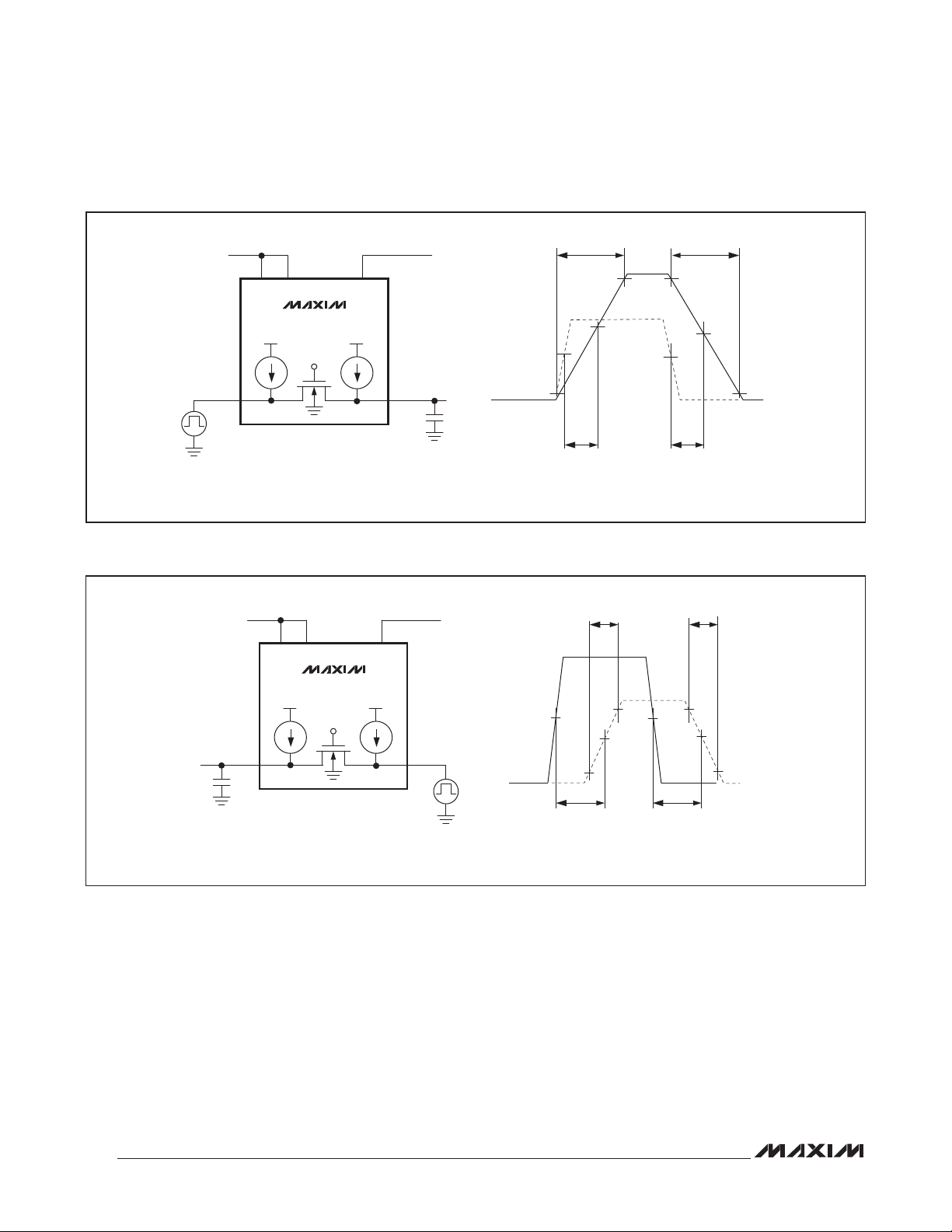
NOTE: THE INPUT RISE/FALL TIMES ARE < 2ns FOR HIGH SPEED AND < 6ns FOR LOW SPEED.
Figure 1. Push-Pull Driving I/O VL_ Test Circuit and Timing
V
MAX14548E/MAX14548AE
L
V
EN
L
V
CC
MAX14548E
MAX14548AE
C
IOVCC
I/O V
V
L
L_
V
CC
I/O V
CC_
V
CC
I/O V
CC_
10%
50%
50%
10%
I/O V
t
PLH
t
RVCC
90%
L_
t
PVL-VCC
t
RVL
50%
50%
= t
I/O V
90%
PLH
CC_
OR t
PHL
50%
t
50%
90%
50%
PLH
t
FVCC
t
90%
FVL
50%
10%
I/O V
10%
L_
NOTE: THE INPUT RISE/FALL TIMES ARE < 2ns FOR HIGH SPEED AND < 6ns FOR LOW SPEED.
Figure 2. Push-Pull Driving I/O V
6
Test Circuit and Timing
CC_
t
PLH
t
PVCC-VL = tPLH OR tPHL
t
PLH
Page 7

100Mbps, 16-Channel LLTs
MAX14548E/MAX14548AE
SOURCE
SOURCE
SOURCE
R
LOAD
EN
I/O V
L_
V
L
MAX14548E
V
MAX14548AE
L
EN
MAX14548E
V
L
MAX14548AE
I/O V
L_
EN
MAX14548E
V
L
MAX14548AE
I/O V
L_
C
IOVL
I/O V
I/O V
I/O V
I/O V
EN
L_
CC_
EN
L_
CC_
t’
EN-VCC
VCC/2
t”
EN-VCC
VCC/2
t
IS WHICHEVER IS LARGER BETWEEN t'
EN-VCC
I/O V
I/O V
EN
CC_
L_
t’
VL /2
EN-VL
V
CC
I/O V
CC_
R
LOAD
C
IOVCC
V
CC
V
CC
V
CC
I/O V
CC_
R
C
LOAD
I/O V
IOVCC
CC_
V
CC
EN-VCC
V
L
O
V
L
O
V
CC
O
V
L
O
V
L
O
V
CC
O
AND t"
V
L
O
V
CC
O
V
L
O
EN-VCC
.
EN
V
L
SOURCE
I/O V
R
LOAD
L_
C
IOVL
Figure 3. Enable Test and Timing
MAX14548E
V
L
MAX14548AE
V
CC
I/O V
CC_
EN
I/O V
CC_
I/O V
L_
t
IS WHICHEVER IS LARGER BETWEEN t'
EN-VL
t”
VL /2
EN-VL
EN-VL
V
L
O
V
CC
O
V
L
O
AND t"
EN-VL
.
7
Page 8
100Mbps, 16-Channel LLTs
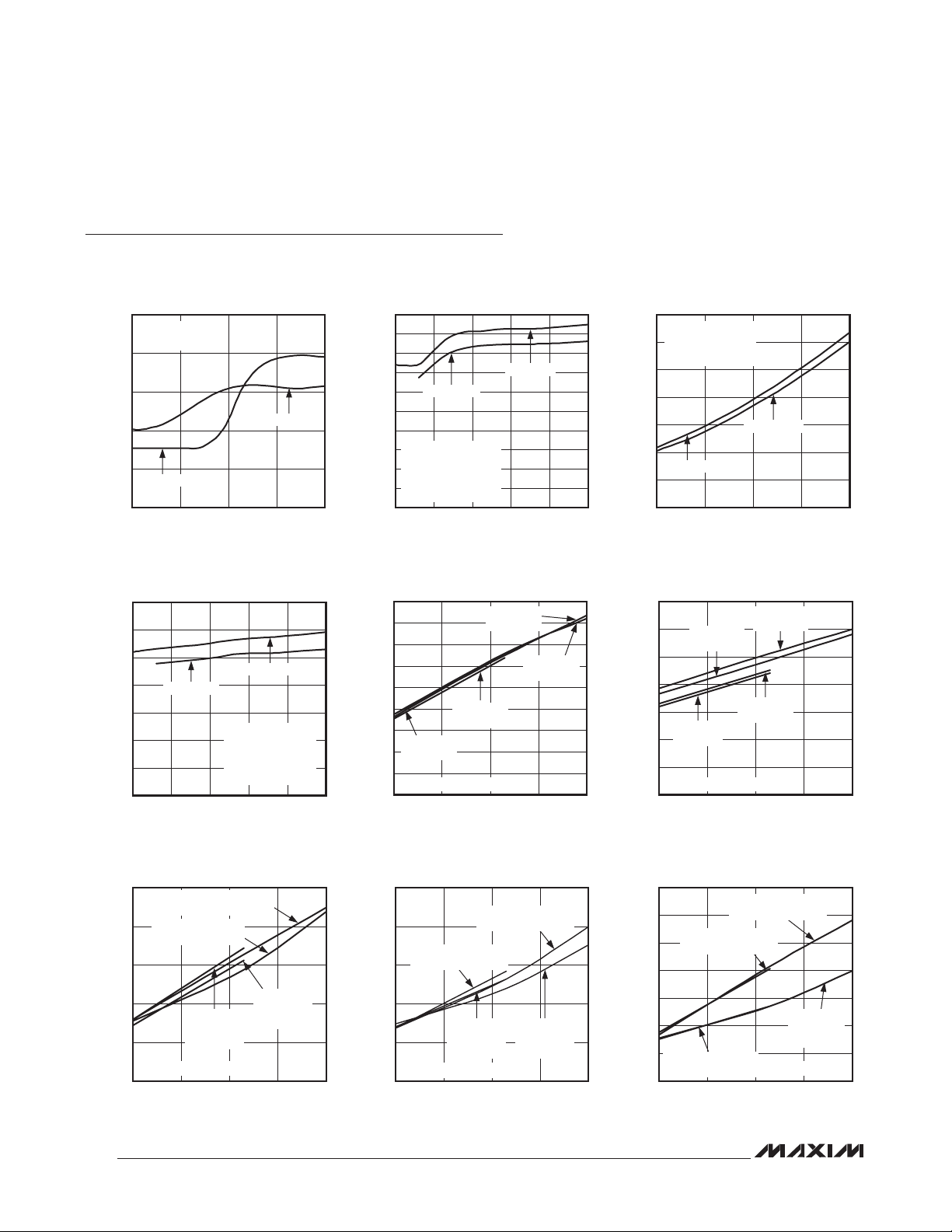
Typical Operating Characteristics
(VCC = 1.8V, VL = 1.4V, CL = 15pF, R
SOURCE
= 150I, data rate = 100Mbps, push-pull driver, TA = +25NC, unless otherwise noted.)
VL SUPPLY CURRENT vs. VCC SUPPLY
VOLTAGE (DRIVING ONE I/O V
250
C
= 15pF
LOAD
PF = LOW
200
150
100
SUPPLY CURRENT (µA)
L
V
50
MAX14548E
0
1.700 3.600
VCC SUPPLY VOLTAGE (V)
L_
MAX14548AE
3.1252.6502.175
)
MAX14548E toc01
VCC SUPPLY CURRENT vs. VL SUPPLY
VOLTAGE (DRIVING ONE I/O V
7
MAX14548E/MAX14548AE
6
5
4
MAX14548AE
3
SUPPLY CURRENT (mA)
2
CC
V
1
0
VL SUPPLY VOLTAGE (V)
MAX14548E
VCC = 3.6V
= 15pF
C
LOAD
PF = HIGH
DATA RATE = 40Mbps
2.62.11.61.1 3.6
)
CC_
MAX14548E toc04
3.1
VCC SUPPLY CURRENT vs. VL SUPPLY
VOLTAGE (DRIVING ONE I/O V
5.0
4.5
4.0
3.5
3.0
2.5
2.0
SUPPLY CURRENT (mA)
1.5
CC
V
1.0
0.5
MAX14548AE
VCC = 3.6V
C
LOAD
PF = LOW
DATA RATE = 40Mbps
0
= 15pF
1.6 2.1 2.6 3.11.1 3.6
VL SUPPLY VOLTAGE (V)
VL SUPPLY CURRENT vs. CAPACITIVE LOAD
(DRIVING ONE I/O V
1800
1600
1400
1200
1000
800
600
SUPPLY CURRENT (µA)
L
MAX14548AE
V
400
200
DATA RATE = 40Mbps
0
MAX14548E
PF LOW
PF LOW
CAPACITIVE LOAD (pF)
MAX14548E
MAX14548E
PF HIGH
MAX14548AE
)
CC_
)
CC
PF HIGH
40302010 50
7
6
MAX14548E toc02
5
4
3
SUPPLY CURRENT (mA)
2
CC
V
1
0
3500
3000
MAX14548E toc05
2500
2000
1500
SUPPLY CURRENT (µA)
L
1000
V
500
0
VCC SUPPLY CURRENT vs. VCC SUPPLY
VOLTAGE (DRIVING ONE I/O V
C
= 15pF
LOAD
PF = HIGH
DATA RATE = 40Mbps
MAX14548AE
MAX14548E
VCC SUPPLY VOLTAGE (V)
)
L_
3.1252.6502.1751.700 3.600
VCC SUPPLY CURRENT vs. CAPACITIVE
LOAD (DRIVING ONE I/O V
MAX14548E
MAX14548AE
PF HIGH
MAX14548E
PF LOW
DATA RATE = 40Mbps
CAPACITIVE LOAD (pF)
PF HIGH
MAX14548AE
PF LOW
)
L_
40302010 50
MAX14548E toc03
MAX14548E toc06
RISE TIME vs. CAPACITIVE LOAD
ON I/O V
2.5
2.0
MAX14548E (PF HIGH)
1.5
1.0
RISE TIME (ns)
0.5
DATA RATE = 40Mbps
0
10 50
(DRIVING ONE I/O VL)
CC
MAX14548AE (PF HIGH)
t
FVCC
t
RVCC
MAX14548AE
(PF LOW)
CAPACITIVE LOAD (pF)
8
t
FVCC
MAX14548E
t
RVCC
(PF LOW)
403020
FALL TIME vs. CAPACITIVE LOAD
ON I/O V
2.5
2.0
MAX14548E toc07
MAX14548AE (PF LOW)
1.5
1.0
FALL TIME (ns)
0.5
DATA RATE = 40Mbps
0
10 50
(DRIVING ONE I/O VL)
CC
t
FVCC
MAX14548AE (PF HIGH)
t
RVCC
t
RVCC
MAX14548E
(PF LOW)
CAPACITIVE LOAD (pF)
MAX14548E
t
FVCC
(PF HIGH)
403020
MAX14548E toc08
RISE TIME (ns)
RISE TIME vs. CAPACITIVE LOAD
ON I/O V
3.5
3.0
2.5
2.0
1.5
1.0
0.5
MAX14548E (PF LOW)
0
(DRIVING ONE I/O VCC)
L
MAX14548AE (PF HIGH)
t
RVL
MAX14548AE (PF LOW)
t
RVL
CAPACITIVE LOAD (pF)
t
FVL
t
FVL
MAX14548E
(PF HIGH)
DATA RATE = 40Mbps
40302010 50
MAX14548E toc09
Page 9

100Mbps, 16-Channel LLTs
Typical Operating Characteristics (continued)
(VCC = 1.8V, VL = 1.4V, CL = 15pF, R
SOURCE
= 150I, data rate = 100Mbps, push-pull driver, TA = +25NC, unless otherwise noted.)
MAX14548E/MAX14548AE
FALL TIME vs. CAPACITIVE LOAD
ON I/O VL (DRIVING ONE I/O VCC)
2.5
2.0
MAX14548E (PF HIGH)
1.5
1.0
FALL TIME (ns)
0.5
DATA RATE = 40Mbps
0
10 50
MAX14548AE
(PF LOW)
CAPACITIVE LOAD (pF)
t
FVL
MAX14548AE (PF HIGH)
t
FVL
t
RVL
t
RVL
MAX14548E
(PF LOW)
403020
PROPAGATION DELAY vs. CAPACITIVE LOAD
ON I/O V
4.5
t
PVCC-VL
MAX14548E
4.0
(PF HIGH)
3.5
3.0
2.5
2.0
1.5
PROPAGATION DELAY (ns)
1.0
0.5
DATA RATE = 40Mbps
0
(DRIVING ONE I/O VCC)
L
t
PVCC-VL
MAX14548E
(PF LOW)
t
PVCC-VL
MAX14548AE
(PF LOW)
CAPACITIVE LOAD (pF)
t
PVCC-VL
MAX14548AE
(PF HIGH)
40302010 50
PROPAGATION DELAY vs. CAPACITIVE
LOAD ON I/O V
4.0
t
PVL-VCC
MAX14548E
3.5
MAX14548E toc10
(PF LOW)
3.0
2.5
2.0
1.5
PROPAGATION DELAY (ns)
1.0
0.5
DATA RATE = 40Mbps
0
(DRIVING ONE I/O VL)
CC
t
PVL-VCC
MAX14548AE
(PF LOW)
t
PVL-VCC
MAX14548AE
(PF HIGH)
CAPACITIVE LOAD (pF)
t
PVL-VCC
MAX14548E
(PF HIGH)
40302010 50
MAX14548E toc11
TYPICAL I/O VL_ DRIVING
(DATA RATE = 100Mbps, C
PF = LOW, MAX14548E
MAX14548E toc12
10ns/div
IOVCC
= 10pF),
MAX14548E toc13
I/O V
1V/div
I/O V
1V/div
L
CC
TYPICAL I/O VL_ DRIVING
(DATA RATE = 40Mbps, C
PF = HIGH, MAX14548E
20ns/div
IOVCC
= 47pF),
MAX14548E toc14
I/O V
1V/div
I/O V
1V/div
TYPICAL I/O V
(DATA RATE = 100Mbps, C
PF = LOW, MAX14548E
L
CC
CC_
10ns/div
DRIVING
= 10pF),
IOVL
MAX14548E toc15
I/O V
1V/div
I/O V
1V/div
CC
L
9
Page 10

100Mbps, 16-Channel LLTs
Typical Operating Characteristics (continued)
(VCC = 1.8V, VL = 1.4V, CL = 15pF, R
SOURCE
= 150I, data rate = 100Mbps, push-pull driver, TA = +25NC, unless otherwise noted.)
TYPICAL I/O V
(DATA RATE = 40Mbps, C
PF = HIGH, MAX14548E
20ns/div
CC_
DRIVING
= 47pF),
IOVL
MAX14548E toc16
I/O V
1V/div
I/O V
1V/div
CC
L
TYPICAL I/O VL_ DRIVING
(DATA RATE = 40Mbps, C
PF = HIGH, MAX14548AE
IOVCC
= 47pF),
MAX14548E toc18
MAX14548E/MAX14548AE
I/O V
L
1V/div
I/O V
CC
1V/div
TYPICAL I/O VL_ DRIVING
(DATA RATE = 100Mbps, C
PF = LOW, MAX14548AE
10ns/div
TYPICAL I/O V
CC_
(DATA RATE = 100Mbps, C
PF = LOW, MAX14548AE
IOVCC
DRIVING
IOVL
MAX14548E toc19
= 10pF),
MAX14548E toc17
= 10pF),
I/O V
1V/div
I/O V
1V/div
I/O V
1V/div
I/O V
1V/div
L
CC
CC
L
10
20ns/div
TYPICAL I/O V
CC_
(DATA RATE = 40Mbps, C
PF = HIGH, MAX14548AE
20ns/div
DRIVING
= 47pF),
IOVL
MAX14548E toc20
I/O V
1V/div
I/O V
1V/div
10ns/div
CC
L
Page 11

100Mbps, 16-Channel LLTs
Pin Configuration
TOP VIEW
(BUMPS ON BOTTOM)
+
A
B
C
GND GNDV
D
E
1
2 3 4
V
CC
L
MAX14548E
MAX14548AE
5 6 7 8
I/O V
4I/O VL3I/O VL2I/O VL1 I/O VL8I/O VL7I/O VL6I/O VL5
L
I/O VL12I/O VL11I/O VL10I/O VL9 I/O VL16I/O VL15I/O VL14I/O VL13
ENV
I/O VCC4I/O VCC3I/O VCC2I/O VCC1 I/O VCC8I/O VCC7I/O VCC6I/O VCC5
I/O VCC12I/O VCC11I/O VCC10I/O VCC9 I/O VCC16I/O VCC15I/O VCC14I/O VCC13
PF
V
CC
L
MAX14548E/MAX14548AE
WLP
(2.16mm
× 3.46mm)
Pin Description
PIN NAME FUNCTION
A1 I/O VL1 Input/Output 1. Referenced to VL.
A2 I/O VL2 Input/Output 2. Referenced to VL.
A3 I/O VL3 Input/Output 3. Referenced to VL.
A4 I/O VL4 Input/Output 4. Referenced to VL.
A5 I/O VL5 Input/Output 5. Referenced to VL.
A6 I/O VL6 Input/Output 6. Referenced to VL.
A7 I/O VL7 Input/Output 7. Referenced to VL.
A8 I/O VL8 Input/Output 8. Referenced to VL.
B1 I/O VL9 Input/Output 9. Referenced to VL.
B2 I/O VL10 Input/Output 10. Referenced to VL.
B3 I/O VL11 Input/Output 11. Referenced to VL.
B4 I/O VL12 Input/Output 12. Referenced to VL.
B5 I/O VL13 Input/Output 13. Referenced to VL.
B6 I/O VL14 Input/Output 14. Referenced to VL.
B7 I/O VL15 Input/Output 15. Referenced to VL.
B8 I/O VL16 Input/Output 16. Referenced to VL.
C1, C8 GND Ground
11
Page 12

100Mbps, 16-Channel LLTs
Pin Description (continued)
PIN NAME FUNCTION
C2, C7 V
C3, C6 V
C4 EN Enable Input. Drive EN to GND for shutdown mode, or drive EN to VL or VCC for normal operation.
C5 PF
D1 I/O VCC1 Input/Output 1. Referenced to VCC.
D2 I/O VCC2 Input/Output 2. Referenced to VCC.
D3 I/O VCC3 Input/Output 3. Referenced to VCC.
D4 I/O VCC4 Input/Output 4. Referenced to VCC.
D5 I/O VCC5 Input/Output 5. Referenced to VCC.
D6 I/O VCC6 Input/Output 6. Referenced to VCC.
D7 I/O VCC7 Input/Output 7. Referenced to VCC.
D8 I/O VCC8 Input/Output 8. Referenced to VCC.
E1 I/O VCC9 Input/Output 9. Referenced to VCC.
MAX14548E/MAX14548AE
E2 I/O VCC10 Input/Output 10. Referenced to VCC.
E3 I/O VCC11 Input/Output 11. Referenced to VCC.
E4 I/O VCC12 Input/Output 12. Referenced to VCC.
E5 I/O VCC13 Input/Output 13. Referenced to VCC.
E6 I/O VCC14 Input/Output 14. Referenced to VCC.
E7 I/O VCC15 Input/Output 15. Referenced to VCC.
E8 I/O VCC16 Input/Output 16. Referenced to VCC.
CC
Logic Supply Voltage, +1.1V to +3.6V. Bypass VL to GND with a 1FF capacitor placed as close as
L
possible to the device.
Power-Supply Voltage, +1.7V to +3.6V. Bypass VCC to GND with a 0.1FF ceramic capacitor. For full
ESD protection, connect an additional 1FF ceramic capacitor from VCC to GND as close as possible
to the VCC input.
Programmable Frequency Input. Drive PF low for high-frequency operation. Drive PF high for lower
frequency operation.
12
Page 13

100Mbps, 16-Channel LLTs
Functional Diagram
I/O VL1
I/O V
I/O V
V
L
MAX14548E
MAX14548AE
2
L
15
L
V
CC
I/O V
1
CC
I/O V
2
CC
15
I/O V
CC
The devices feature a programmable frequency input
(PF) that guarantees a bit rate of 100Mbps with a load
capacitance < 15pF and VL > 1.1V (MAX14548E) or VL >
1.4V (MAX14548AE) when driven low. The MAX14548E
can drive capacitive loads up to 50pF with a guaranteed
bit rate of 40Mbps when VL R 1.1V and PF is driven high.
The MAX14548AE can drive capacitive loads up to 50pF
with a guaranteed bit rate of 40Mbps when VL R 1.1V and
PF is driven high.
Level Translation
For proper operation, ensure that 1.7V P VCC P 3.6V,
1.1V P VL P VCC. When power is supplied to VL while
VCC is less than VL, the devices automatically enter a
low-power mode and the I/Os are in high-impedance
mode. The devices also enter shutdown mode when
EN = 0. In both conditions where EN = 0 or VL > VCC,
there is a known high-impedance state on I/O VL_and
I/O V
. The maximum data rate depends heavily on
CC_
the load capacitance (see the rise/fall time graphs in the
Typical Operating Characteristics), output impedance of
the driver, and the operating voltage range.
MAX14548E/MAX14548AE
I/O V
16
L
EN
PF
GND
I/O V
16
CC
Detailed Description
The MAX14548E/MAX14548AE 16-channel, bidirectional
level translators (LLTs) provide the level shifting necessary for 100Mbps data transfer in multivoltage systems.
Externally applied voltages, VCC and VL, set the logic
levels on either side of the device. Logic signals present
on the VL side of the device appear as a high-voltage
logic signal on the VCC side of the device and vice versa.
The devices operate at full speed with external drivers
that source as little as 4mA output current (min). Each
I/O channel is pulled up to VCC or VL by an internal
35FA current source, allowing the devices to be driven
by either push-pull or open-drain drivers.
The devices feature an enable input (EN) that places the
device into a low-power shutdown mode when driven
low. They also feature an automatic shutdown mode that
disables the part when VCC is less than VL.
Input Driver Requirements
The device architecture is based on an nMOS pass gate
and output accelerator stages (Figure 4). The accelerators are active only when there is a rising/falling edge on
a given I/O. A short pulse is then generated where the
output accelerator stages become active and charge/
discharge the capacitances at the I/Os. Due to its architecture, both input stages become active during the
one-shot pulse. This can lead to some current feeding
into the external source that is driving the translator.
However, this behavior helps speed up the transition on
the driven side.
The devices have internal current sources capable of
sourcing 35FA to pull up the I/O lines. These internal
pullup current sources allow the inputs to be driven with
open-drain drivers and push-pull drivers. It is not recommended to use external pullup resistors on the I/O lines.
The architecture of the devices permit either side to be
driven with a minimum of 4mA drivers or larger.
Output Load Requirements
The device I/Os are designed to drive CMOS inputs.
Do not load the I/O lines with a resistive load less than
25kI and do not place an RC circuit at the input of
these devices to slow down the edges. If a slower rise/
fall time is required, refer to the MAX3000E/MAX3001E/
MAX3002–MAX3012 data sheet.
13
Page 14

100Mbps, 16-Channel LLTs
V
L
ENABLE
I/O V
L_
NOTE 1: THE MAX14548E/MAX14548AE ARE ENABLED WHEN VL <
Figure 4. Simplified Functional Diagram for One I/O Line
MAX14548E/MAX14548AE
Shutdown Mode
30µA
V
L
BOOST
CIRCUIT
V
L
BOOST
CIRCUIT
The EN input places the devices into a low-power shutdown mode when driven low. The automatic shutdown
mode disables the devices when VCC is unconnected or
less than VL. When VCC is less than VL or EN = GND, the
devices enter shutdown mode.
Data Rate and Capacitive Load (PF Input)
The programmable frequency input (PF) adjusts the oneshot accelerator to guarantee a 100Mbps bit rate with a
load capacitance <15pF and VL > 1.1V (MAX14548E)
or VL > 1.4V (MAX14548AE) when driven low. The
MAX14548E can drive capacitive loads up to 50pF with
a guaranteed 40Mbps bit rate when VL > 1.1V and PF
is driven high. The MAX14548AE can drive capacitive
loads up to 50pF with a guaranteed 40Mbps bit rate
when VL > 1.1V and PF is driven high.
V
CC
ENABLE
ENABLE
30µA
V
CC
V
CC
VCC - 0.2V
I/O V
AND EN = VL.
CC_
Applications Information
Layout Recommendations
Use standard high-speed layout practices when laying
out a board with the MAX14548E/MAX14548AE. For
example, to minimize line coupling, place all other signal
lines not connected to the devices at least 1x the substrate height of the PCB away from the input and output
lines of the devices.
Power-Supply Decoupling
To reduce ripple and the chance of introducing data
errors, bypass VL and VCC to ground with 0.1FF ceramic
capacitors. Place all capacitors as close as possible to
the power-supply inputs. For full ESD protection, bypass
VCC with a 1FF ceramic capacitor located as close as
possible to the VCC input.
14
Page 15

100Mbps, 16-Channel LLTs
R
C
1MΩ
CHARGE-CURRENT-
LIMIT RESISTOR
HIGH-
VOLTAGE
DC
SOURCE
Figure 5a. Human Body ESD Test Model Figure 5b. Human Body Current Waveform
100pF
C
s
R
D
1500Ω
DISCHARGE
RESISTANCE
STORAGE
CAPACITOR
DEVICE
UNDER
TEST
AMPS
IP 100%
90%
36.8%
10%
PEAK-TO-PEAK RINGING
I
r
(NOT DRAWN TO SCALE)
0
0
t
RL
TIME
t
DL
CURRENT WAVEFORM
MAX14548E/MAX14548AE
Unidirectional vs. Bidirectional Level
Translator
The devices bidirectional level translators can operate as
a unidirectional device by selecting one I/O as the input
and the corresponding I/O as an output. These devices
provide the smallest solution (WLP package) for level
translation applications.
ESD Protection
As with all Maxim devices, ESD-protection structures are
incorporated on all pins to protect against electrostatic
discharges encountered during handling and assembly.
The I/O VL_ and I/O V
pins have extra protection
CC_
against static electricity.
ESD Test Conditions
ESD performance depends on a variety of conditions.
Contact Maxim for a reliability report that documents test
setup, test methodology, and test results.
Human Body Model
Figure 5a shows the Human Body Model, and Figure
5b shows the current waveform it generates when discharged into a low impedance. This model consists of a
100pF capacitor charged to the ESD voltage of interest,
which is then discharged into the test device through a
1.5kI resistor.
Use with External Pullup/Pulldown
Resistors
Due to the architecture of the devices, it is not recommended to use external pullup or pulldown resistors
on the bus. In certain applications, the use of external
pullup or pulldown resistors is desired to have a known
bus state when there is no active driver on the bus. The
devices include internal pullup current sources that set
the bus state when the device is enabled. In shutdown
mode, the state of I/O V
and I/O VL_ is high imped-
CC_
ance.
Open-Drain Signaling
The devices are designed to pass open-drain as well
as CMOS push-pull signals. When used with open-drain
signaling, the rise time is dominated by the interaction
of the internal pullup current source and the parasitic
load capacitance. The devices include internal rise time
accelerators to speed up transitions, eliminating any
need for external pullup resistors. For applications such
as I2C or 1-WireM that require an external pullup resistor,
refer to the MAX13046E and MAX13047E data sheets.
1-Wire is a registered trademark of Maxim Integrated
Products, Inc.
15
Page 16

100Mbps, 16-Channel LLTs
Typical Operating Circuit
+1.8V
1µF
EN
I/O V
V
LVCC
MAX14548A
MAX14548AE
L_
+1.8V
SYSTEM
CONTROLLER
PF PF
EN
DATA
16
Chip Information
PROCESS: BiCMOS
MAX14548E/MAX14548AE
+2.8V
1µF 0.1µF
+2.8V
SYSTEM
DATA
16
GNDGND GND
I/O V
CC_
Package Information
For the latest package outline information and land patterns,
go to www.maxim-ic.com/packages. Note that a “+”, “#”, or
“-” in the package code indicates RoHS status only. Package
drawings may show a different suffix character, but the drawing
pertains to the package regardless of RoHS status.
PACKAGE TYPE PACKAGE CODE DOCUMENT NO.
40 WLP W402B3+1
21-0437
16
Page 17

100Mbps, 16-Channel LLTs
Revision History
MAX14548E/MAX14548AE
REVISION
NUMBER
0 4/10 Initial release —
REVISION
DATE
DESCRIPTION
PAGES
CHANGED
Maxim cannot assume responsibility for use of any circuitry other than circuitry entirely embodied in a Maxim product. No circuit patent licenses are implied.
Maxim reserves the right to change the circuitry and specifications without notice at any time.
Maxim Integrated Products, 120 San Gabriel Drive, Sunnyvale, CA 94086 408-737-7600 17
©
2010 Maxim Integrated Products Maxim is a registered trademark of Maxim Integrated Products, Inc.
 Loading...