

For free samples & the latest literature: http://www.maxim-ic.com, or phone 1-800-998-8800.
For small orders, phone 408-737-7600 ext. 3468.
General Description
The MAX1450 sensor signal conditioner is optimized for
piezoresistive sensor calibration and temperature compensation. It includes an adjustable current source for
sensor excitation and a 3-bit programmable-gain amplifier (PGA). Achieving a total typical error factor within
1% of the sensor’s inherent repeatability errors, the
MAX1450 compensates offset, full-span output (FSO), offset tempco, FSO tempco, and FSO nonlinearity of silicon
piezoresistive sensors via external trimmable resistors,
potentiometers, or digital-to-analog converters (DACs).
The MAX1450 is capable of compensating sensors that
display close error distributions with a single temperature point, making it ideal for low-cost, medium-accuracy
applications. Although optimized for use with popular
piezoresistive sensors, it may also be used with other
resistive sensor types such as strain gauges.
Customization
Maxim can customize the MAX1450 for unique requirements including improved power specifications. With a
dedicated cell library consisting of more than 90 sensor-specific functional blocks, Maxim can quickly provide customized MAX1450 solutions. Contact the
factory for additional information.
Applications
Piezoresistive Pressure and Acceleration
Transducers and Transmitters
Manifold Absolute Pressure (MAP) Sensors
Automotive Systems
Hydraulic Systems
Industrial Pressure Sensors
Features
♦ 1% Sensor Signal Conditioning
♦ Corrects Sensor Errors Using Coefficients Stored
in External Trimmable Resistors, Potentiometers,
or DACs
♦ Compensates Offset, Offset TC, FSO, FSO TC,
and FSO Linearity
♦ Rail-to-Rail
®
Analog Output
♦ Programmable Current Source for Sensor
Excitation
♦ Fast Signal-Path Settling Time (< 1ms)
♦ Accepts Sensor Outputs from 10mV/V to 30mV/V
♦ Fully Analog Signal Path
MAX1450
Low-Cost, 1%-Accurate Signal Conditioner
for Piezoresistive Sensors
________________________________________________________________
Maxim Integrated Products
1
PGA
A = 1
OUT
ISRC
BDRIVE
INP
INM
SOTC
SOFF
OFFTC
OFFSET
BBUF
A2
FSOTRIM
A1
A0
+
-
V
DD
V
SS
CURRENT
SOURCE
V
DD
MAX1450
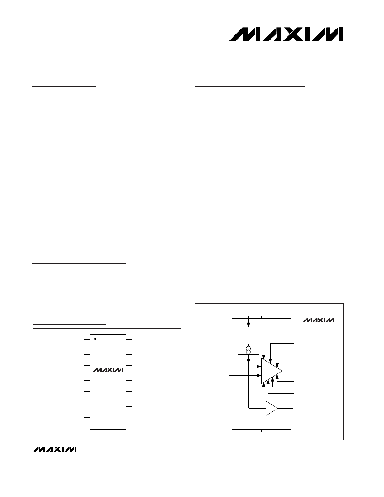
Pin Configuration
19-1365; Rev 0; 5/98
PART
MAX1450CAP
MAX1450C/D
MAX1450EAP -40°C to +85°C
0°C to +70°C
0°C to +70°C
TEMP. RANGE PIN-PACKAGE
20 SSOP
Dice*
20 SSOP
*
Dice are tested at TA = +25°C, DC parameters only.
Functional Diagram
Ordering Information
Rail-to-Rail is a registered trademark of Nippon Motorola, Ltd.
查询MAX1450供应商
TOP VIEW
INP
I.C.
I.C.
SOFF
A1
A0
OFFSET
20
INM
19
V
SS
18
BDRIVE
17
ISRCSOTC
16
I.C.
15
V
DD
OUT
14
A2OFFTC
13
12
I.C.
11
FSOTRIMBBUF
1
2
3
4
MAX1450
5
6
7
8
9
10
SSOP

MAX1450
Low-Cost, 1%-Accurate Signal Conditioner
for Piezoresistive Sensors
2 _______________________________________________________________________________________
ABSOLUTE MAXIMUM RATINGS
ELECTRICAL CHARACTERISTICS
(VDD= +5V, VSS= 0, TA= T
MIN
to T
MAX
, unless otherwise noted. Typical values are at TA= +25°C.)
Stresses beyond those listed under “Absolute Maximum Ratings” may cause permanent damage to the device. These are stress ratings only, and functional
operation of the device at these or any other conditions beyond those indicated in the operational sections of the specifications is not implied. Exposure to
absolute maximum rating conditions for extended periods may affect device reliability.
Supply Voltage, VDDto VSS......................................-0.3V to +6V
All Other Pins ...................................(VSS- 0.3V) to (VDD+ 0.3V)
Short-Circuit Duration, OUT, BBUF, BDRIVE.............Continuous
Continuous Power Dissipation (TA= +70°C)
SSOP (derate 8.00mW/°C above +70°C) ....................640mW
Operating Temperature Range
MAX1450CAP .....................................................0°C to +70°C
MAX1450EAP ..................................................-40°C to +85°C
Storage Temperature Range.............................-65°C to +165°C
Lead Temperature (soldering, 10sec).............................+300°C
TA= +25°C (Note 1)
DC to 10Hz, gain = 39,
sensor impedance = 5kΩ
V
OUT
= (VSS+ 0.25V) to (VDD- 0.25V)
,
TA= +25°C
(Note 5)
(Note 4)
5kΩ load to VSSor V
DD,
TA= +25°C
From VSSto V
DD
63% of final value
(Notes 2, 3)
Eight selectable gains (Table 3)
CONDITIONS
µV
RMS
500Output Noise
mA
-1.0 1.0
(sink) (source)
Output Current Range
V
V
SS +
V
DD -
0.25 0.25
Output Voltage Swing
V/V36 39 44
Minimum Differential Signal
Gain
V/V39 to 221Differential Signal Range Gain
mA2.8 3.5I
DD
Supply Current
mV/V10 to 30
Input-Referred Adjustable
Full-Span Output Range
mV±100
Input-Referred Adjustable Offset
Range
dB90CMRRCommon-Mode Rejection Ratio
ms1Output Step-Response Time
MΩ1.0R
IN
Input Impedance
µV/°C±0.5
Input-Referred Offset
Temperature Coefficient
%V
DD
0.01Amplifier Gain Nonlinearity
UNITSMIN TYP MAXSYMBOLPARAMETER
No load, TA= T
MIN
to T
MAX
V
SS +
V
DD -
0.05 0.05
V4.5 5.0 5.5V
DD
Supply Voltage
At any gain ppm/°C±50
Differential Signal Path
Temperature Coefficient
V/V1.15Offset TC Gain
V/V1.15Offset Gain
∆∆V
V
OUT
OFFSET
∆∆V
V
OUT
OFFTC
GENERAL CHARACTERISTICS
ANALOG OUTPUT (PGA)
ANALOG INPUT (PGA)
SUMMING JUNCTION (Figure 1)

MAX1450
Low-Cost, 1%-Accurate Signal Conditioner
for Piezoresistive Sensors
_______________________________________________________________________________________
3
ELECTRICAL CHARACTERISTICS (continued)
(VDD= +5V, VSS= 0, TA= T
MIN
to T
MAX
, unless otherwise noted. Typical values are at TA= +25°C.)
Note 1: Contact factory for high-volume applications requiring less than 1.5mA.
Note 2: All electronics temperature errors are compensated together with the sensor errors.
Note 3: The sensor and the MAX1450 must always be at the same temperature during calibration and use.
Note 4: This is the maximum allowable sensor offset at minimum gain (39V/V).
Note 5: This is the sensor’s sensitivity normalized to its drive voltage, assuming a desired full-span output (FSO) of 4V and a bridge
voltage of 2.5V. Operating at lower bridge excitation voltages can accommodate higher sensitivities.
V
BDRIVE
= 2.5V
No load
(V
BDRIVE
- V
BBUF
) at V
BDRIVE
= 2.5V, no load
CONDITIONS
µA-100 100Current Drive
V
V
SS +
V
DD -
1.3 1.3
Voltage Swing
mV-20 20V
OFS
Offset Voltage
UNITSMIN TYP MAXSYMBOLPARAMETER
∆I
BDRIVE/
∆I
ISRC
(Figure 2)
V
V
SS +
V
DD -
1.3 1.3
V
BDRIVE
Bridge Voltage Swing
mA0.1 0.5 2.0I
BDRIVE
Bridge Current Range
µA/µA13AACurrent-Source Gain
V
V
SS +
V
DD-
1.3 1.3
V
ISRC
Current-Source Input Voltage
Range
BUFFER (BBUF)
CURRENT SOURCE
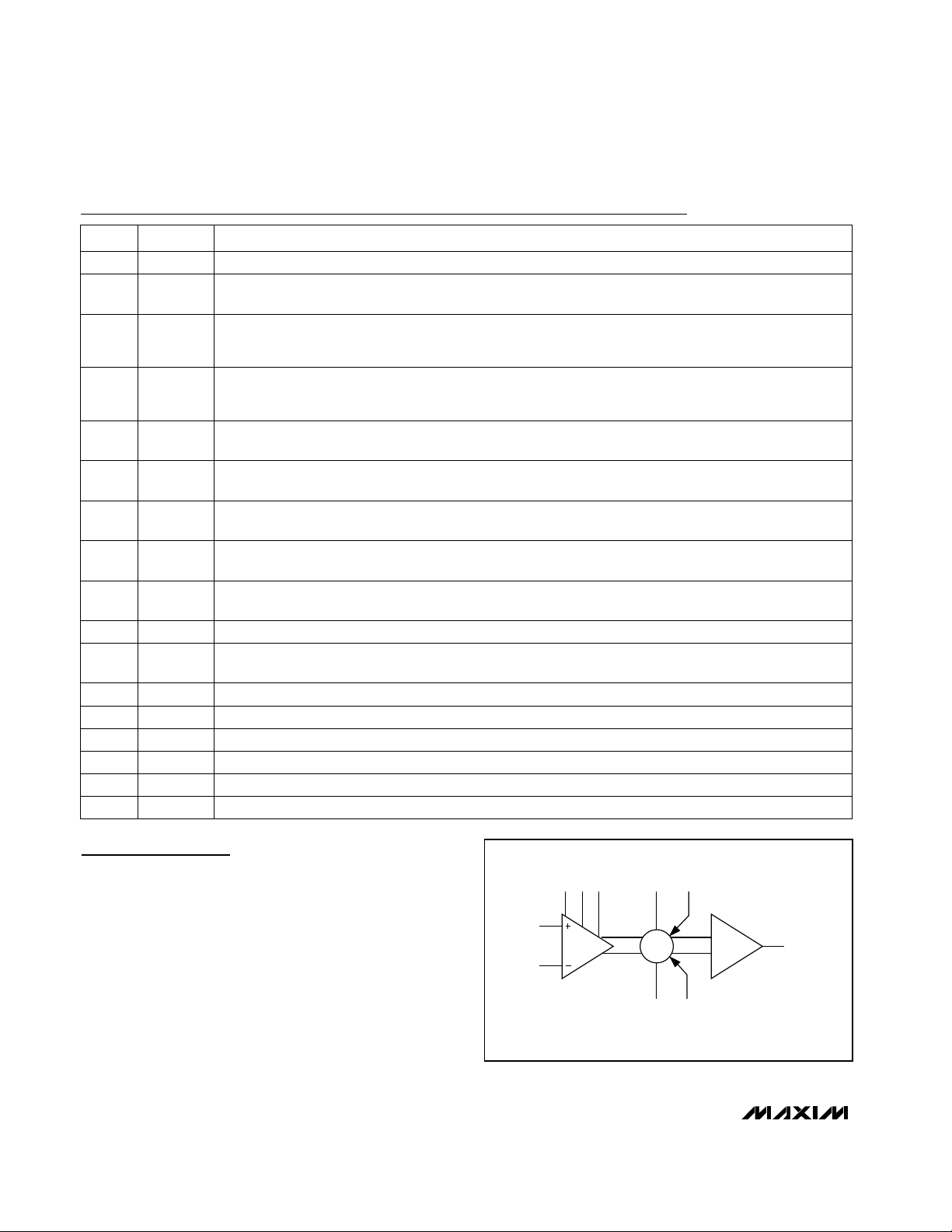
______________ Detailed Description
Analog Signal Path
The MAX1450’s signal path is fully differential and combines the following three stages: a 3-bit PGA with
selectable gains of 39, 65, 91, 117, 143, 169, 195, and
221; a summing junction; and a differential to singleended output buffer (Figure 1).
Programmable-Gain Amplifier
The analog signal is first fed into a programmable-gain
instrumentation amplifier with a CMRR of 90dB and a
common-mode input range from VSSto VDD. Pins A0,
A1, and A2 set the PGA gain anywhere from 39V/V to
221V/V (in steps of 26).
MAX1450
Low-Cost, 1%-Accurate Signal Conditioner
for Piezoresistive Sensors
4 _______________________________________________________________________________________
NAME FUNCTION
1 INP Positive Sensor Input. Input impedance is typically 1MΩ. Rail-to-rail input range.
PIN
2, 3,
12, 16
I.C. Internally connected. Leave unconnected.
4 SOTC
Offset TC Sign Bit Input. A logic low inverts V
OFFTC
with respect to V
SS.
This pin is internally pulled to V
SS
via a 1MΩ (typical) resistor. Connect to VDDto add V
OFFTC
to the PGA output, or leave unconnected (or
connect to VSS) to subtract V
OFFTC
from the PGA output.
8 OFFTC
Offset TC Adjust. Analog input summed with PGA output and V
OFFSET
. Input impedance is typically 1MΩ.
Rail-to-rail input range.
7 A0
PGA Gain-Set LSB Input. Internally pulled to VSSvia a 1MΩ (typical) resistor. Connect to VDDfor a logic
high or VSSfor a logic low.
6 A1
PGA Gain-Set Input. Internally pulled to VSSvia a 1MΩ (typical) resistor. Connect to VDDfor a logic high or
VSSfor a logic low.
5 SOFF
Offset Sign Bit Input. A logic low inverts V
OFFSET
with respect to VSS. This pin is internally pulled to VSSvia
a 1MΩ (typical) resistor. Connect to VDDto add V
OFFSET
to the PGA output, or leave unconnected (or con-
nect to VSS) to subtract V
OFFSET
from the PGA output.
14 OUT PGA Output Voltage. Connect a 0.1µF capacitor from OUT to VSS.
13 A2
PGA Gain-Set MSB Input. Internally pulled to VSSvia a 11kΩ (typical) resistor. Connect to VDDfor a logic
high or VSSfor a logic low.
11 FSOTRIM Bridge Drive Current-Set Input. The voltage on this pin sets the nominal I
ISRC
. See the
Bridge Drive
section.
10 BBUF
Buffered Bridge-Voltage Output (the voltage at BDRIVE). Use with correction resistor R
STC
to correct for FSO
tempco.
9 OFFSET
Offset Adjust Input. Analog input summed with PGA output and V
OFFTC
. Input impedance is typically
1MΩ. Rail-to-rail input range.
Pin Description
15 V
DD
Positive Supply Voltage Input. Connect a 0.1µF capacitor from VDDto VSS.
20 INM Negative Sensor Input. Input impedance is typically 1MΩ. Rail-to-rail input range.
19 V
SS
Negative Power-Supply Input.
18 BDRIVE Sensor Excitation Current Output. This pin drives a nominal 0.5mA through the bridge.
17 ISRC Current-Source Reference. Connect a 50kΩ (typical) resistor from ISRC to VSS.
Figure 1. Signal-Path Functional Diagram
INP
INM
A2
A1 A0
PGA
OFFTC SOTC
±
Σ
±
OFFSET SOFF
A = 1
OUT

Summing Junction
The second stage in the analog signal path consists of
a summing junction for offset, offset temperature compensation, and the PGA output. The offset voltage
(V
OFFSET
) and offset temperature-compensation volt-
age (V
OFFTC
) add or subtract from the PGA output
depending on their respective sign bits, offset sign
(SOFF), and offset TC sign (SOTC). V
OFFSET
and
V
OFFTC
can range in magnitude from VSSto VDD.
Output Buffer
The final stage in the analog signal path consists
of a unity-gain buffer. This buffer is capable of swinging
to within 250mV of VSSand VDDwhile sourcing/sinking
up to 1.0mA, or within 50mV of the power supplies with
no load.
Bridge Drive
Figure 2 shows the functional diagram of the on-chip
current source. The voltage at FSOTRIM, in conjunction
with R
ISRC
, sets the nominal current, I
ISRC
which sets
the FSO (refer to Figure 3 for sensor terminology.) I
ISRC
is additionally modulated by components from the
external resistor R
STC
and the optional resistor R
LIN
.
R
STC
is used to feed back a portion of the buffered
bridge-excitation voltage (V
BBUF
), which compensates
FSO TC errors by modulating the bridge-excitation current over temperature. To correct FSO linearity errors,
feed back a portion of the output voltage to the currentsource reference node via the optional R
LIN
resistor.
Applications Information
Compensation Procedure
The following compensation procedure assumes a pressure transducer with a +5V supply and an output voltage
that is ratiometric to the supply voltage (see
Ratiometric
Output Configuration
section). The desired offset voltage
(V
OUT
at P
MIN
) is 0.5V, and the desired FSO voltage
(V
OUT(PMAX
) - V
OUT(PMIN
)) is 4V; thus the FS output volt-
age (V
OUT
at P
MAX
) will be 4.5V. The procedure requires
a minimum of two test pressures (e.g., zero and full scale)
and two temperatures. A typical compensation procedure
is as follows:
1) Perform Coefficient Initialization
2) Perform FSO Calibration
3) Perform FSO TC Compensation
4) Perform OFFSET TC Compensation
5) Perform OFFSET Calibration
6) Perform Linearity Calibration (Optional)
Coefficient Initialization
Select the resistor values and the PGA gain to prevent
gross overload of the PGA and bridge current source.
These values depend on sensor behavior and require
some sensor characterization data. This data may be
available from the sensor manufacturer. If not, it can be
generated by performing a two-temperature, two-pres-
MAX1450
Low-Cost, 1%-Accurate Signal Conditioner
for Piezoresistive Sensors
_______________________________________________________________________________________ 5
V
DD
I
BDRIVE ≈
13 (I
ISRC
)
V
BDRIVE
I
ISRC
I
ISRC
BBUF
INP
INM
SENSOR
R
ISRC
(EXTERNAL)
BDRIVE
FSOTRIM
BBUF
OUT
A = 1
R
STC
(EXTERNAL)
R
LIN
(OPTIONAL)
(EXTERNAL)
MAX1450
Figure 2. Bridge Drive Circuit

MAX1450
sure sensor evaluation. Note that the resistor values
and PGA gain obtained from this evaluation will represent a starting point. The final compensated transducer
will likely use slightly different values. The required sensor information is shown in Table 1, and can be used to
obtain the values for the parameters shown in Table 2.
Selecting R
ISRC
R
ISRC
programs the nominal sensor excitation current
and is placed between ISRC and VSS. Use a variable
resistor with a nominal starting value of:
where Rb(T1) is the sensor input impedance at temperature T1 (usually +25°C).
Selecting R
STC
R
STC
compensates the FSO TC errors and is placed
between BBUF and ISRC. Use a variable resistor with
a nominal starting value of the following:
This approximation works best for bulk, micromachined,
silicon piezoresistive sensors (PRTs). Negative values
for R
STC
indicate unexpected sensor behavior that cannot be compensated by the MAX1450 without additional external circuitry.
Selecting PGA Gain Setting
Calculate the ideal gain using the following formula,
and select the nearest gain setting from Table 3.
SensorFSO can be derived as follows:
where S is the sensor sensitivity at T1, V
BDRIVE
is the
sensor excitation voltage (initially 2.5V), and ∆P is the
maximum pressure differential.
SensorFSO S x V x P
1.5mV/V psi x 2.5V x 10 psi
0.0375V
BDRIVE
=
=
=
∆
R
R x 500ppm/ C
TCR TCS
65k x 500ppm/ C
2600ppm/ C 2100ppm/ C
65k
STC
ISRC
≈
°
−
≈
°
− −
=
Ω
Ω
o o
R 13 x Rb(T1)
13(5k ) 65k
ISRC
≈
≈ =Ω Ω
Low-Cost, 1%-Accurate Signal Conditioner
for Piezoresistive Sensors
6 _______________________________________________________________________________________
Table 1. Sensor Information
Table 2.Compensation Components/Values
PARAMETER
SENSOR
DESCRIPTION
TYPICAL
VALUE
Rb(T) Input/Output Impedance 5kΩ at +25°C
TCR
Input/Output Impedance
Tempco
2600ppm/°C
S(T) Sensitivity
1.5mV/V psi at
+25°C
TCS Sensitivity Tempco -2100ppm/°C
O(T) Offset
12mV/V at
+25°C
OTC Offset Tempco
-1030 ppmFSO/°C
S(p)
Sensitivity Linearity Error as
% FSO BSLF (Best StraightLine Fit)
0.1% FSO
BSLF
P
MIN
Minimum Input Pressure 0 PSI
P
MAX
Maximum Input Pressure 10 PSI
PARAMETER DESCRIPTION
R
ISRC
Resistor that programs the nominal sensor
excitation current
R
STC
Resistor that compensates FSO TC errors
A
PGA
Programmable-gain amplifier gain
OFFTC
Offset TC correction voltage, including its
respective sign bit
R
LIN
Resistor that corrects FSO linearity errors
(optional)
Figure 3. Typical Pressure-Sensor Output
4.5
FULL-SPAN OUTPUT (FSO)
VOLTAGE (V)
0.5
OFFSET
P
MIN
PRESSURE
P
MAX
FULL-SCALE (FS)
where OUTFSO is the desired calibrated transducer
full-span output voltage, and SensorFSO is the sensor
full-span output voltage at T1.
Determining OFFTC Initial Value
Generally, the OFFTC coefficient can be set to 0V,
since the offset TC errors will be compensated in a later
step. However, sensors with large offset TC errors may
require an initial coarse offset TC adjustment to prevent
the PGA from saturating as the temperature increases
during the compensation procedure. An initial coarse
offset TC adjustment would be required if the magnitude of the sensor offset TC error is more than about
10% of the FSO. If a coarse offset TC adjustment is
required, use the following equation:
which can be approximated by:
where OTC is the sensor offset TC error in ppm of FSO,
∆T is the operating temperature range in °C, and OTC
Correction is the offset TC resistor-divider ratio. For
positive values of OTC correction, connect SOTC to
V
DD
; for negative values, connect SOTC to VSS.
Select the Offset TC resistor divider (R
OTCA
and
R
OTCB
, Figure 4) using the following equation:
where 500kΩ ≥ (R
OTCA
+ R
OTCB
) ≥ 100kΩ. Choose
R
OTCB
= 100kΩ and R
OTCA
= 20kΩ.
Transfer Function
The following transfer function (linearity correction not
included) is useful for data modeling or for developing
compensative algorithms:
(AA = current source gain)
FSO Calibration
Perform FSO calibration at room temperature with a fullscale sensor excitation.
1) At +25°C (or T1), set V
FSOTRIM
to 2.5V. Adjust
R
ISRC
until V
BBUF
= 2.5V.
2) Adjust V
OFFSET
until the room temperature offset
voltage is 0.5V (see
OFFSET Calibration
section).
3) Measure the full-span output (measuredV
FSO
).
4) Calculate V
BIDEAL(25°C)
using the following equation:
Note: If V
BIDEAL(25°C)
is outside the allowable bridge
voltage swing of (VSS+ 1.3V) to (VDD- 1.3V), readjust
the PGA gain setting. If V
BIDEAL(25°C)
is too low,
decrease the PGA gain setting by one step and return
to Step 1. If V
BIDEAL(25°C)
is too high, increase the PGA
gain setting by one step and return to Step 1.
V
V 1
desiredV measuredV
measuredV
BIDEAL(25 C)
FSOTRIM
FSO FSO
FSO
o
=
+
[ ]−[ ]
[ ]
V V x
V x PGA + 1.15 x
V
V
1.15 x V
where V =
V
R
V
R
1
AA x Rb(T)
1
R
OUT BDRIVE
S
OFFTC
DD
OFFSET
BDRIVE
DD
ISRC
DD
STC
STC
=
+
+
+
OTC Correction
R
R R
R
R R
OTCA
OTCA OTCB
OTCA
OTCA OTCB
.
=
+
=
+
0 17
OTC Correction
OTC x FSO x ( T)
TCS x V x 1.15 x ( T)
1
2100 x .5V x 1.15
0.68
BDRIVE
≈
≈
− °
−
=
∆
∆
030 4
2
ppm C x V/
OTC Correction
V
V x 1.15
OUT(T)
BDRIVE(T)
=
∆
∆
A
OUTFSO
SensorFSO
4V
0.0375V
106V/V
PGA
≈
≈ =
MAX1450
Low-Cost, 1%-Accurate Signal Conditioner
for Piezoresistive Sensors
_______________________________________________________________________________________ 7
Table 3. PGA Gain Settings
PGA GAIN (V/V) PGA VALUE A2 A1 A0
39 0 0 0 0
65 1 0 0 1
91 2 0 1 0
117 3 0 1 1
143 4 1 0 0
169 5 1 0 1
195 6 1 1 0
221 7 1 1 1

MAX1450
5) Set V
FSOTRIM
= V
BIDEAL(25°C)
. Adjust R
ISRC
until
V
BBUF
= V
BIDEAL(25°C)
.
6) Readjust V
OFFSET
until the offset voltage is 0.5V (see
OFFSET Calibration
section).
FSO TC Compensation
Correct linear span TC by connecting BBUF to ISRC
through a resistor (R
STC
). The value of R
STC
depends
on the required correction coefficient, which is sensor
dependent, but typically around 100kΩ for most silicon
PRTs. The following procedure results in FSO TC calibration:
1) Measure the full-span output at T2.
2) Use the equation from Step 4 of the
FSO Calibration
section to determine V
BIDEAL(T2)
. While at T2, adjust
R
STC
until V
BBUF
= V
BIDEAL(T2)
.
3) Do not adjust V
OFFSET
or V
OFFTC
.
OFFSET TC Compensation
Connect OFFTC to a resistor divider between BBUF
and VSS. The divided-down V
BBUF
is then fed into
OFFTC and the appropriate polarity (designating
whether V
OFFTC
should be added or subtracted from
the PGA output) is selected with SOTC.
1) At T2, remeasure the offset at V
OUT
.
2) Use the following equation to determine the magnitude of V
OFFTC(T2)
, and adjust R
OTCA
accordingly. If
V
OFFTC
is negative, connect SOTC to VSS. If V
OFFTC
is positive, connect SOTC to VDD. After OTC calibration, the output may be saturated; correct this condition during OFFSET calibration. In most cases
Current OFFTC will be 0. However, if a coarse
OFFTC adjustment was performed, the coefficient
must be inserted in the equation below.
where Current OFFTC is the voltage at pin OFFTC.
Note that the magnitude of V
OFFTC
is directly proportional to the gain of the PGA. Therefore, if the PGA gain
changes after performing the offset TC calibration, the
offset TC must be recalibrated.
V
V V
V V x 1.15
Current OFFTC
OFFTC
OFFSET(T1) OFFSET(T2)
BDRIVE(T1) BDRIVE(T2)
=
−
−
( )
+
Low-Cost, 1%-Accurate Signal Conditioner
for Piezoresistive Sensors
8 _______________________________________________________________________________________
R
STC
R
FSOB
R
FSOA
V
DD
V
DD
R
ISRC
0.1µF
R
LIN
(OPTIONAL)
PGA
A = 1
CURRENT
SOURCE
OUT
OUT
ISRC
BDRIVE
INP
INM
SOTC
OFFSET
OFFTC
SOFF
BBUF
A2
A1
A0
V
DD
V
DD
FSOTRIM
V
SS
MAX1450
R
OTCA
R
OTCB
R
OFFA
R
OFFB
V
DD
V
DD
0.1µF
0.1µF
SENSOR
V
DD
Figure 4. Basic Ratiometric Output Configuration

OFFSET Calibration
Accomplish offset calibration by applying a voltage to the
OFFSET pin (SOFF determines the polarity of V
OFFSET
).
This voltage is generated by a resistor-divider between
VDDand VSS(R
OFFA
and R
OFFB
in Figure 4). To calibrate
the offset, set V
OFFSET
to 0 and perform a minimum pressure input reading at room temperature. If the output voltage (V
OFFZERO
) is greater than 0.5V, connect SOFF to
VSS; if V
OFFZERO
is less than 0.5V, connect SOFF to VDD.
Adjust V
OFFSET
until V
OUT
= 0.5V.
Note that the magnitude of V
OFFSET
is directly proportional to the gain of the PGA. Therefore, if the PGA gain
changes after performing the offset calibration, the offset
must be recalibrated.
Linearity Calibration (optional)
Correct pressure linearity by using feedback from the
output voltage (V
OUT
) to ISRC to modulate the current
source. If a bridge current is constant with applied
pressure, sensor linearity remains unaffected. If, with a
constant bridge current, the output voltage is nonlinear
with applied pressure (e.g., increasing faster than the
pressure), use pressure linearity correction to linearize
the output.
Performing linearity corrections through the use of a
transfer function is not practical, since a number of
required system variables cannot easily be measured
with a high enough degree of accuracy. Therefore, use a
simple empirical approach. Figure 5 shows the uncompensated pressure linearity error of a silicon PRT. The
magnitude of this error is usually well below 1% of span.
Curves A, B, C, D, E, and F in Figure 5 represent increasing amounts of linearity error corrections, corresponding
to decreasing values in the resistance of R
LIN
. To correct
pressure linearity errors, use the following equation to
determine the appropriate range for R
LIN
:
where S(p) is the sensitivity linearity error as % best
straight-line fit (BSLF). Ideally, this variable resistor
should be disconnected during temperature error compensation. If this is not possible, set it to the maximum
available value.
First measure the magnitude of the uncorrected error
(R
LIN
= maximum value), then choose an arbitrary
value for R
LIN
(approximately 50% of maximum value).
Measuring the new linearity error establishes a linear
relationship between the amount of linearity correction
and the value of R
LIN
.
Note that if pressure linearity correction is to be performed, it must occur after temperature compensation
is completed. A minor readjustment to the FSO and
OFFSET will be required after linearity correction is performed. If pressure linearity correction is not required,
remove R
LIN
.
Ratiometric Output Configuration
Ratiometric output configuration provides an output that
is proportional to the power-supply voltage. When used
with ratiometric A/D converters, this output provides
digital pressure values independent of supply voltage.
Most automotive and some industrial applications
require ratiometric outputs.
The MAX1450 has been designed to provide a highperformance ratiometric output with a minimum number
of external components (Figure 4).
Sensor Calibration and
Compensation Example
Calibration and compensation requirements for a sensor
involve conversion of a sensor-specific performance
into a normalized output curve. Table 4 shows an
example of the MAX1450’s capabilities.
A repeatable piezoresistive sensor with an initial offset
of 30mV and FSO of 37.5mV was converted into a compensated transducer (using the piezoresistive sensor
with the MAX1450) with an offset of 0.5V and an FSO of
4.0V. The temperature errors, which were on the order
of -17% for the offset TC and -35% for the FSO TC, were
reduced to about ±1% FSO. The graphs of Figure 6
show the outputs of the uncompensated sensor and the
compensated transducer.
R
R x R
R R x S p
LIN
ISRC STC
ISRC STC
≈
+
( )
( )
2
MAX1450
Low-Cost, 1%-Accurate Signal Conditioner for
Piezoresistive Sensors
_______________________________________________________________________________________ 9
B
C
D
E
F
PRESSURE
LINEARITY
ERROR
UNCOMPENSATED ERROR
(R
LIN
REMOVED)
OVERCOMPENSATED ERROR
(R
LIN
TOO SMALL)
A
Figure 5. Effect of R
LIN
on Linearity Corrections

MAX1450
Low-Cost, 1%-Accurate Signal Conditioner
for Piezoresistive Sensors
10 ______________________________________________________________________________________
-20
-10
10
0
20
30
-50 0 50 100 150
UNCOMPENSATED SENSOR ERROR
TEMPERATURE (°C)
ERROR (% SPAN)
OFFSET
FSO
-0.8
-0.6
0.4
-0.2
-0.4
0
0.2
0.6
0.8
-50 0 50 100 150
COMPENSATED TRANSDUCER ERROR
TEMPERATURE °(C)
ERROR (% SPAN)
OFFSET
FSO
Figure 6. Comparison of an Uncalibrated Sensor and a Temperature-Compensated Transducer
TRANSISTOR COUNT: 1364
SUBSTRATE CONNECTED TO V
SS
Chip Information
Typical Uncompensated Input (Sensor) Typical Compensated Transducer Output
Offset ..........................................................................±80% FSO
FSO..................................................................................15mV/V
Offset TC......................................................................-17% FSO
Offset TC Nonlinearity.....................................................1% FSO
FSO TC.........................................................................-35% FSO
FSO TC Nonlinearity........................................................1% FSO
Temperature Range...........................................-40°C to +125°C
V
OUT
...................................................Ratiometric to VDDat 5.0V
Offset at +25°C ......................................................0.500V ±5mV
FSO at +25°C .........................................................4.000V ±5mV
Offset Accuracy Over Temp. Range.............±60mV (1.5% FSO)
FSO Accuracy Over Temp. Range ...............±60mV (1.5% FSO)
Table 4. MAX1450 Calibration and Compensation

MAX1450
Low-Cost, 1%-Accurate Signal Conditioner for
Piezoresistive Sensors
______________________________________________________________________________________ 11
Package Information
SSOP.EPS

MAX1450
Low-Cost, 1%-Accurate Signal Conditioner
for Piezoresistive Sensors
Maxim cannot assume responsibility for use of any circuitry other than circuitry entirely embodied in a Maxim product. No circuit patent licenses are
implied. Maxim reserves the right to change the circuitry and specifications without notice at any time.
12
____________________Maxim Integrated Products, 120 San Gabriel Drive, Sunnyvale, CA 94086 408-737-7600
© 1998 Maxim Integrated Products Printed USA is a registered trademark of Maxim Integrated Products.
NOTES

Copyright © Each Manufacturing Company.
All Datasheets cannot be modified without permission.
This datasheet has been download from :
www.AllDataSheet.com
100% Free DataSheet Search Site.
Free Download.
No Register.
Fast Search System.
www.AllDataSheet.com
 Loading...