

Page 1
General Description
The MAX1438 octal, 12-bit analog-to-digital converter
(ADC) features fully differential inputs, a pipelined
architecture, and digital error correction incorporating a
fully differential signal path. This ADC is optimized for
low-power and high-dynamic performance in medical
imaging instrumentation and digital communications
applications. The MAX1438 operates from a 1.8V single
supply and consumes only 913mW (114mW per channel) while delivering a 69.9dB (typ) signal-to-noise ratio
(SNR) at a 5.3MHz input frequency. In addition to low
operating power, the MAX1438 features a power-down
mode for idle periods.
An internal 1.24V precision bandgap reference sets the
full-scale range of the ADC. A flexible reference structure allows the use of an external reference for applications requiring increased accuracy or a different input
voltage range. The reference architecture is optimized
for low noise.
A single-ended clock controls the data-conversion
process. An internal duty-cycle equalizer compensates
for wide variations in clock duty cycle. An on-chip PLL
generates the high-speed serial low-voltage differential
signal (LVDS) clock.
The MAX1438 has self-aligned serial LVDS outputs for
data, clock, and frame-alignment signals. The output
data is presented in two’s complement or binary format.
The MAX1438 offers a maximum sample rate of
65Msps. See the
Pin-Compatible Versions
table below
for lower-speed versions. This device is available in a
small, 14mm x 14mm x 1mm, 100-pin TQFP package
with exposed pad and is specified for the extended
industrial (-40°C to +85°C) temperature range.
Applications
Ultrasound and Medical Imaging
Instrumentation
Multichannel Communications
Features
o Excellent Dynamic Performance
69.9dB SNR at 5.3MHz
95dBc SFDR at 5.3MHz
85dB Channel Isolation
o Ultra-Low Power
114mW per Channel (Normal Operation)
o Serial LVDS Outputs
o Pin-Selectable LVDS/SLVS (Scalable Low-Voltage
Signal) Mode
o LVDS Outputs Support Up to 30 Inches FR-4
Backplane Connections
o Test Mode for Digital Signal Integrity
o Fully Differential Analog Inputs
o Wide Differential Input Voltage Range (1.4V
P-P
)
o On-Chip 1.24V Precision Bandgap Reference
o Clock Duty-Cycle Equalizer
o Compact, 100-Pin TQFP Package with Exposed
Pad
o Evaluation Kit Available (Order MAX1438EVKIT)
MAX1438
Octal, 12-Bit, 65Msps, 1.8V ADC
with Serial LVDS Outputs
________________________________________________________________
Maxim Integrated Products
1
Ordering Information
19-0359; Rev 1; 2/11
For pricing, delivery, and ordering information, please contact Maxim Direct at 1-888-629-4642,
or visit Maxim’s website at www.maxim-ic.com.
Pin Configuration appears at end of data sheet.
EVALUATION KIT
AVAILABLE
Pin-Compatible Versions
+
Denotes a lead(Pb)-free/RoHS-compliant package.
D = Dry pack.
*
EP = Exposed pad.
PART TEMP RANGE PIN-PACKAGE
MAX1438ECQ+D -40°C to +85°C
100 TQFP-EP*
(14mm x 14mm x 1mm)
PART
MAX1434 50 10
MAX1436 40 12
MAX1437 50 12
MAX1438 65 12
SAMPLING RATE
(Msps)
RESOLUTION
(BITS)
Page 2
MAX1438
Octal, 12-Bit, 65Msps, 1.8V ADC
with Serial LVDS Outputs
2 _______________________________________________________________________________________
ABSOLUTE MAXIMUM RATINGS
Stresses beyond those listed under “Absolute Maximum Ratings” may cause permanent damage to the device. These are stress ratings only, and functional
operation of the device at these or any other conditions beyond those indicated in the operational sections of the specifications is not implied. Exposure to
absolute maximum rating conditions for extended periods may affect device reliability.
(Voltages referenced to GND)
AVDD.....................................................................-0.3V to +2.0V
CVDD.....................................................................-0.3V to +3.6V
OVDD ....................................................................-0.3V to +2.0V
IN_P, IN_N ..............................................-0.3V to (V
AVDD
+ 0.3V)
CLK ........................................................-0.3V to (V
CVDD
+ 0.3V)
OUT_P, OUT_N, FRAME_, CLKOUT_ ....-0.3V to (V
OVDD
+ 0.3V)
DT, SLVS/LVDS, LVDSTEST, PLL_, T/B,
REFIO, REFADJ, CMOUT...................-0.3V to (V
AVDD
+ 0.3V)
Continuous Power Dissipation (T
A
= +70°C)
TQFP (derate 47.6mW/°C above +70°C)................3809.5mW
Operating Temperature Range ...........................-40°C to +85°C
Maximum Junction Temperature .....................................+150°C
Storage Temperature Range .............................-65°C to +150°C
Lead Temperature (soldering, 10s) .................................+300°C
Soldering Temperature (reflow) .......................................+260°C
ELECTRICAL CHARACTERISTICS
(V
AVDD
= 1.8V, V
OVDD
= 1.8V, V
CVDD
= 3.3V, V
GND
= 0V, external V
REFIO
= 1.24V, C
REFIO
= 0.1µF, C
REFP
= 10µF, C
REFN
= 10µF,
f
CLK
= 65MHz (50% duty cycle), VDT= 0V, TA= T
MIN
to T
MAX
, unless otherwise noted. Typical values are at TA= +25°C.) (Notes 2, 3)
PACKAGE THERMAL CHARACTERISTICS (Note 1)
TQFP
Junction-to-Ambient Thermal Resistance (θ
JA
) ...........21°C/W
Junction-to-Case Thermal Resistance (θ
JC
) ..................2°C/W
Note 1: Package thermal resistances were obtained using the method described in JEDEC specification JESD51-7, using a four-
layer board. For detailed information on package thermal considerations, refer to www.maxim-ic.com/thermal-tutorial.
PARAMETER SYMBOL CONDITIONS MIN TYP MAX UNITS
DC ACCURACY (Note 4)
Resolution N 12 Bits
Integral Nonlinearity INL ±0.4 ±2.5 LSB
Differential Nonlinearity DNL No missing codes over temperature ±0.25 ±1 LSB
Offset Error ±0.5 %FS
Gain Error -3.5 +2.0 %FS
ANALOG INPUTS (IN_P, IN_N)
Input Differential Range V
Common-Mode Voltage Range V
Common-Mode Voltage Range
Tolerance
Differential Input Impedance R
Differential Input Capacitance C
CONVERSION RATE
Maximum Conversion Rate f
Minimum Conversion Rate f
Data Latency 6.5 Cycles
DYNAMIC CHARACTERISTICS (differential inputs, 4096-point FFT) (Note 4)
Signal-to-Noise Ratio SNR
Signal-to-Noise and Distortion
(First 4 Harmonics)
ID
CMO
IN
IN
SMAX
SMIN
SINAD
Differential input 1.4 V
(Note 5) ±50 mV
Switched capacitor load 2 kΩ
fIN = 5.3MHz at -0.5dBFS 69.9
f
= 19.3MHz at -0.5dBFS 66.5 69.6
IN
fIN = 5.3MHz at -0.5dBFS 69.8
= 19.3MHz at -0.5dBFS 66.5 69.6
f
IN
0.76 V
12.5 pF
65 MHz
4.0 MHz
P-P
dB
dB
Page 3
MAX1438
Octal, 12-Bit, 65Msps, 1.8V ADC
with Serial LVDS Outputs
_______________________________________________________________________________________ 3
ELECTRICAL CHARACTERISTICS (continued)
(V
AVDD
= 1.8V, V
OVDD
= 1.8V, V
CVDD
= 3.3V, V
GND
= 0V, external V
REFIO
= 1.24V, C
REFIO
= 0.1µF, C
REFP
= 10µF, C
REFN
= 10µF,
f
CLK
= 65MHz (50% duty cycle), VDT= 0V, TA= T
MIN
to T
MAX
, unless otherwise noted. Typical values are at TA= +25°C.) (Notes 2, 3)
PARAMETER SYMBOL CONDITIONS MIN TYP MAX UNITS
Effective Number of Bits ENOB
Spurious-Free Dynamic Range SFDR
Total Harmonic Distortion THD
Intermodulation Distortion IMD
Third-Order Intermodulation IM3
Aperture Jitter t
Aperture Delay t
Small-Signal Bandwidth SSBW Input at -20dBFS 100 MHz
Full-Power Bandwidth LSBW Input at -0.5dBFS 100 MHz
Output Noise IN_P = IN_N 0.44 LSB
Over-Range Recovery Time t
INTERNAL REFERENCE
REFADJ Internal Reference-Mode
Enable Voltage
REFADJ Low-Leakage Current 1.5 mA
REFIO Output Voltage V
Reference Temperature
Coefficient
EXTERNAL REFERENCE
REFADJ External ReferenceMode Enable Voltage
REFADJ High-Leakage Current 200 µA
REFIO Input Voltage 1.24 V
REFIO Input Voltage Tolerance ±5 %
REFIO Input Current I
COMMON-MODE OUTPUT (CMOUT)
CMOUT Output Voltage V
CLOCK INPUT (CLK)
Input High Voltage V
Input Low Voltage V
Clock Duty Cycle 50 %
Clock Duty-Cycle Tolerance ±30 %
AJ
AD
OR
REFIO
TC
REFIO
REFIO
CMOUT
CLKH
CLKL
fIN = 5.3MHz at -0.5dBFS 11.4
f
= 19.3MHz at -0.5dBFS 11.4
IN
fIN = 5.3MHz at -0.5dBFS 95
f
= 19.3MHz at -0.5dBFS 79 93
IN
fIN = 5.3MHz at -0.5dBFS -98
= 19.3MHz at -0.5dBFS -92 -79
f
IN
f
= 5.3MHz at -6.5dBFS
1
f
= 6.3MHz at -6.5dBFS
2
f
= 5.3MHz at -6.5dBFS
1
f
= 6.3MHz at -6.5dBFS
2
Figure 11 < 0.4 ps
Figure 11 1 ns
RS = 25Ω, CS = 50pF 1
(Note 6) 0.1 V
(Note 6)
1.18 1.24 1.30 V
V
-
AVDD
0.1
0.8 x
V
AVDD
89.3 dBc
97.5 dBc
120 ppm/°C
< 1 µA
0.76 V
0.2 x
V
AVDD
Clock
cycle
dB
dBc
dBc
RMS
RMS
V
V
V
Page 4
MAX1438
Octal, 12-Bit, 65Msps, 1.8V ADC
with Serial LVDS Outputs
4 _______________________________________________________________________________________
ELECTRICAL CHARACTERISTICS (continued)
(V
AVDD
= 1.8V, V
OVDD
= 1.8V, V
CVDD
= 3.3V, V
GND
= 0V, external V
REFIO
= 1.24V, C
REFIO
= 0.1µF, C
REFP
= 10µF, C
REFN
= 10µF,
f
CLK
= 65MHz (50% duty cycle), VDT= 0V, TA= T
MIN
to T
MAX
, unless otherwise noted. Typical values are at TA= +25°C.) (Notes 2, 3)
PARAMETER SYMBOL CONDITIONS MIN TYP MAX UNITS
Input Leakage Current DI
Input Capacitance DC
DIGITAL INPUTS (PLL_, LVDSTEST, DT, SLVS, PD, T/B)
Input Logic-High Voltage V
Input Logic-Low Voltage V
Input Leakage Current DI
Input Capacitance DC
LVDS OUTPUTS (OUT_P, OUT_N), SLVS/LVDS = 0
Differential Output Voltage V
Output Common-Mode Voltage V
Rise Time (20% to 80%) t
Fall Time (80% to 20%) t
SLVS OUTPUTS (OUT_P, OUT_N, CLKOUTP, CLKOUTN, FRAMEP, FRAMEN), SLVS/LVDS = 1, DT = 1
Differential Output Voltage V
Output Common-Mode Voltage V
Rise Time (20% to 80%) t
Fall Time (80% to 20%) t
POWER-DOWN
PD Fall to Output Enable t
PD Rise to Output Disable t
POWER REQUIREMENTS
AVDD Supply Voltage Range V
OVDD Supply Voltage Range V
CVDD Supply Voltage Range V
AVDD Supply Current I
OVDD Supply Current I
CVDD Supply Current I
Power Dissipation P
OHDIFFRTERM
OCMRTERM
RL
FL
OHDIFFRTERM
OCMRTERM
RS
FS
ENABLE
DISABLE
AVDD
OVDD
CVDD
AVDD
OVDD
CVDD
DISSfIN
Input at GND 5
IN
Input at AVDD 80
IN
IH
IL
Input at GND 5
IN
Input at AVDD 80
IN
0.8 x
V
AVDD
= 100Ω 250 450 mV
= 100Ω 1.125 1.375 V
R
TERM
R
TERM
= 100Ω, C
= 100Ω, C
= 5pF 350 ps
LOAD
= 5pF 350 ps
LOAD
= 100Ω 205 mV
= 100Ω 220 mV
R
TERM
R
TERM
= 100Ω, C
= 100Ω, C
= 5pF 320 ps
LOAD
= 5pF 320 ps
LOAD
(Note 7) 100 ms
P D = 0 422 465
fIN = 19.3MHz
at -0.5dBFS
P D = 0, D T = 1 422
P D = 1, p ower - dow n,
no cl ock i np ut
P D = 0 85 110
fIN = 19.3MHz
at -0.5dBFS
P D = 0, D T = 185
P D = 1, p ower - dow n,
no cl ock i np ut
CVDD is used only to bias ESD-protection
diodes on CLK input, Figure 2
= 19.3MHz at -0.5dBFS 913 1035 mW
5pF
0.2 x
V
AVDD
5pF
20 ns
1.7 1.8 1.9 V
1.7 1.8 1.9 V
1.7 1.8 3.6 V
mA
1.16 mA
mA
960 µA
0mA
µA
V
V
µA
Page 5
MAX1438
Octal, 12-Bit, 65Msps, 1.8V ADC
with Serial LVDS Outputs
_______________________________________________________________________________________ 5
ELECTRICAL CHARACTERISTICS (continued)
(V
AVDD
= 1.8V, V
OVDD
= 1.8V, V
CVDD
= 3.3V, V
GND
= 0V, external V
REFIO
= 1.24V, C
REFIO
= 0.1µF, C
REFP
= 10µF, C
REFN
= 10µF,
f
CLK
= 65MHz (50% duty cycle), VDT= 0V, TA= T
MIN
to T
MAX
, unless otherwise noted. Typical values are at TA= +25°C.) (Notes 2, 3)
Note 2: Specifications at TA≥ +25°C are guaranteed by production testing. Specifications at TA< +25°C are guaranteed by design
and characterization and not subject to production testing.
Note 3: All capacitances are between the indicated pin and GND, unless otherwise noted.
Note 4: See definition in the
Parameter Definitions
section at the end of this data sheet.
Note 5: See the
Common-Mode Output (CMOUT)
section.
Note 6: Connect REFADJ to GND directly to enable internal reference mode. Connect REFADJ to AVDD directly to disable the inter-
nal bandgap reference and enable external reference mode.
Note 7: Measured using C
REFP
to GND = 1µF and C
REFN
to GND = 1µF. t
ENABLE
time may be lowered by using smaller capacitor values.
Note 8: Data valid to CLKOUT rise/fall timing is measured from 50% of data output level to 50% of clock output level.
Note 9: Guaranteed by design and characterization. Not subject to production testing.
Typical Operating Characteristics
(V
AVDD
= 1.8V, V
OVDD
= 1.8V, V
CVDD
= 3.3V, V
GND
= 0V, internal reference, differential input at -0.5dBFS, fIN= 5.3MHz, f
CLK
= 65MHz
(50% duty cycle), V
DT
= 0V, C
LOAD
= 10pF, TA= +25°C, unless otherwise noted.)
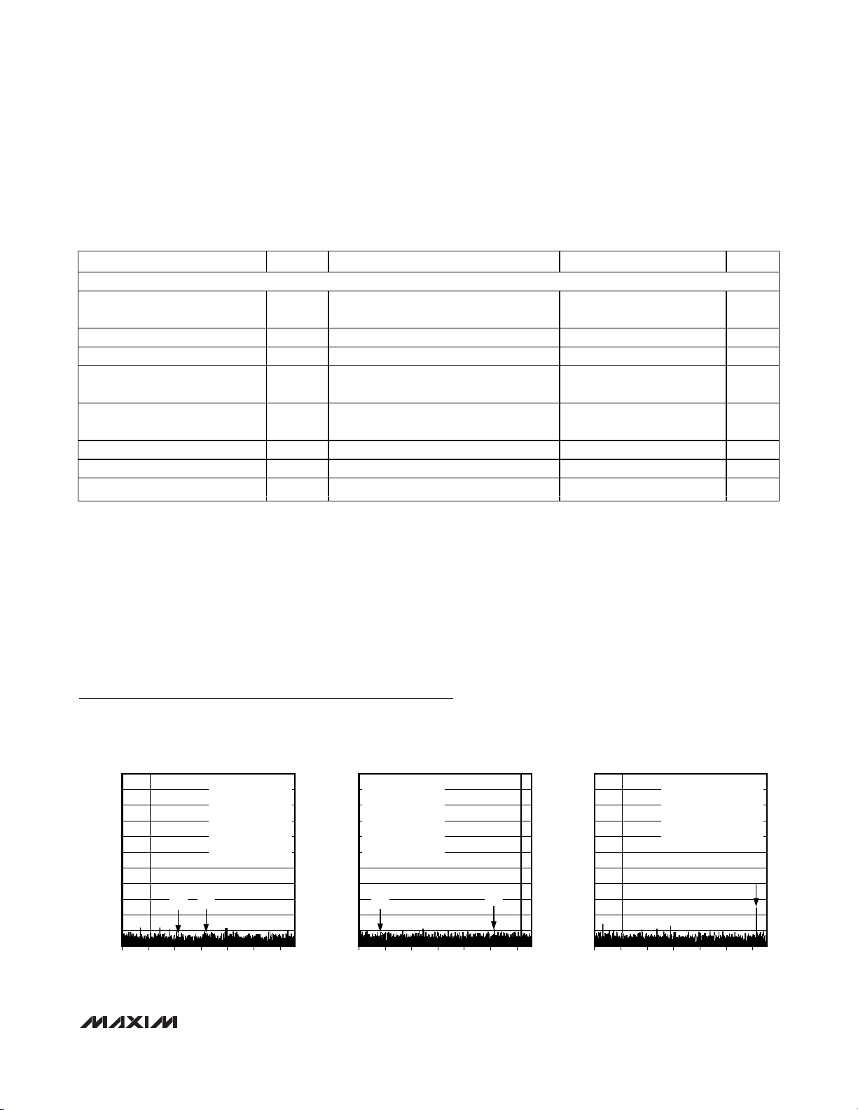
FFT PLOT
(16,384-POINT DATA RECORD)
MAX1438 toc01
FREQUENCY (MHz)
AMPLITUDE (dBFS)
0
-10
-20
-30
-40
-50
-70
-60
-80
-100
-90
-110
0 5 10 15 20 25 30
f
CLK
= 65.4966636MHz
f
IN
= 5.304814MHz
A
IN
= -0.5dBFS
SNR = 70.120dB
SINAD = 70.112dB
THD = -97.686dBc
SFDR = 95.406dBc
HD2
HD3
FFT PLOT
(16,384-POINT DATA RECORD)
MAX1438 toc02
FREQUENCY (MHz)
AMPLITUDE (dBFS)
0
-10
-20
-30
-40
-50
-70
-60
-80
-100
-90
-110
f
CLK
= 65.4966637MHz
f
IN
= 30.313794MHz
A
IN
= -0.5dBFS
SNR = 69.584dB
SINAD = 69.516dB
THD = -97.316dBc
SFDR = 94.713dBc
HD2
HD3
0 5 10 15 20 25 30
CROSSTALK
(16,384-POINT DATA RECORD)
MAX1438 toc03
FREQUENCY (MHz)
AMPLITUDE (dBFS)
0
-10
-20
-30
-40
-50
-70
-60
-80
-100
-110
-90
MEASURED ON CHANNEL 1,
WITH INTERFERING SIGNAL
ON CHANNEL 2
f
IN(IN1)
= 5.304814MHz
f
IN(IN2)
= 30.3189139MHz
CROSSTALK = 85.4dB
f
IN(IN2)
0 5 10 15 20 25 30
PARAMETER SYMBOL CONDITIONS MIN TYP MAX UNITS
TIMING CHARACTERISTICS (Note 8)
Data Valid to CLKOUT Rise/Fall t
CLKOUT Output-Width High t
CLKOUT Output-Width Low t
FRAME Rise to CLKOUT Rise t
Sample CLK Rise to FRAME Rise t
Crosstalk (Note 4) -85 dB
Gain Matching C
Phase Matching C
OD
CH
CL
CF
SF
GMfIN
PMfIN
Figure 5 (Note 9)
Figure 5 t
Figure 5 t
Figure 4 (Note 9)
Figure 4 (Note 9)
( t
S AM P LE
- 0.15
( t
S AM P LE
- 0.15
( t
S AM P LE
+ 1.1
/24)
( t
S AM P LE
/12 ns
S AM P LE
/12 ns
S AM P LE
/24)
( t
S AM P LE
/2)
( t
S AM P LE
+ 0.15
+ 0.15
+ 2.6
/24)
/24)
/2)
ns
ns
ns
= 5.3MHz (Note 4) ±0.1 dB
= 5.3MHz (Note 4) ±0.25 D eg r ees
Page 6
MAX1438
Octal, 12-Bit, 65Msps, 1.8V ADC
with Serial LVDS Outputs
6 _______________________________________________________________________________________
Typical Operating Characteristics (continued)
(V
AVDD
= 1.8V, V
OVDD
= 1.8V, V
CVDD
= 3.3V, V
GND
= 0V, internal reference, differential input at -0.5dBFS, fIN= 5.3MHz, f
CLK
= 65MHz
(50% duty cycle), V
DT
= 0V, C
LOAD
= 10pF, TA= +25°C, unless otherwise noted.)
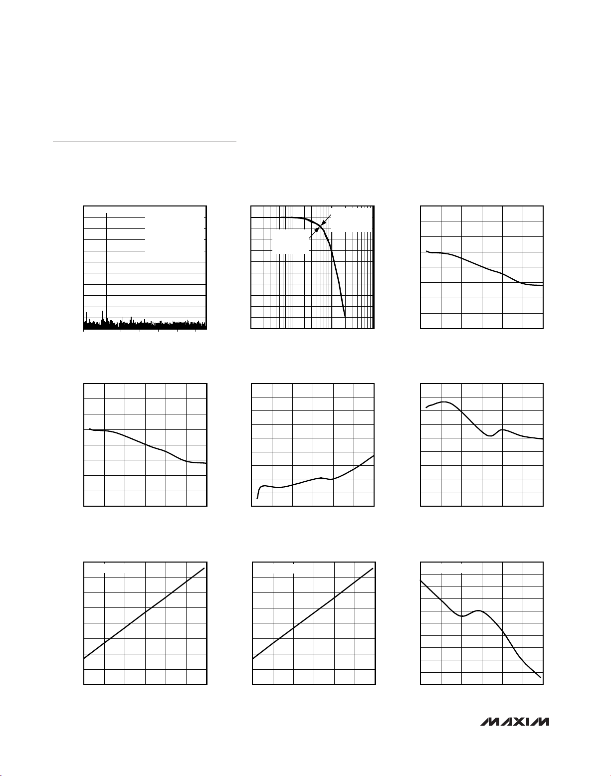
MAX1438 toc04
FREQUENCY (MHz)
AMPLITUDE (dBFS)
0
-10
-20
-30
-40
-50
-70
-60
-80
-100
-90
-110
TWO-TONE INTERMODULATION DISTORTION
(16,384-POINT DATA RECORD)
f
IN(IN1)
= 5.296593MHz
f
IN(IN2)
= 6.299991MHz
A
IN1
= -6.5dBFS
A
IN2
= -6.5dBFS
IMD = 89.3dBc
IM3 = 97.5dBc
0 5 10 15 20 25 30
1
-1
-10
1 100 1000
-6
-7
-8
-9
-5
-4
-3
-2
MAX1438 toc05
ANALOG INPUT FREQUENCY (MHz)
GAIN (dB)
10
BANDWIDTH
vs. ANALOG INPUT FREQUENCY
0
FULL-POWER
BANDWIDTH
-0.5dBFS
SMALL-SIGNAL
BANDWIDTH
-20.5dBFS
SIGNAL-TO-NOISE RATIO
vs. ANALOG INPUT FREQUENCY
f
(MHz)
SNR (dB)
1008020 40 60
72
71
70
69
68
67
66
MAX1438 toc06
73
65
0120
SIGNAL-TO-NOISE PLUS DISTORTION
vs. ANALOG INPUT FREQUENCY
fIN (MHz)
SINAD (dB)
1008020 40 60
72
71
70
69
68
67
66
MAX1438 toc07
73
65
0120
TOTAL HARMONIC DISTORTION
vs. ANALOG INPUT FREQUENCY
fIN (MHz)
THD (dBc)
1008020 40 60
-95
-90
-85
-75
-70
-80
-65
-60
MAX1438 toc08
-55
-100
0120
SPURIOUS-FREE DYNAMIC RANGE
vs. ANALOG INPUT FREQUENCY
fIN (MHz)
SFDR (dBc)
1008020 40 60
60
65
70
80
85
75
90
95
MAX1438 toc09
100
55
0120
SIGNAL-TO-NOISE RATIO
vs. ANALOG INPUT POWER
ANALOG INPUT POWER (dBFS)
SNR (dB)
-5-10-25 -20 -15
37
42
52
57
47
62
67
72
32
-30 0
MAX1438 toc10
fIN = 5.304814MHz
SIGNAL-TO-NOISE PLUS DISTORTION
vs. ANALOG INPUT POWER
ANALOG INPUT POWER (dBFS)
SINAD (dB)
-5-10-25 -20 -15
37
42
52
57
47
62
MAX1438 toc11
67
72
32
-30 0
fIN = 5.304814MHz
TOTAL HARMONIC DISTORTION
vs. ANALOG INPUT POWER
ANALOG INPUT POWER (dBFS)
THD (dBc)
-5-10-25 -20 -15
-85
-90
-80
-70
-65
-75
-60
-55
-50
-100
-95
-30 0
MAX1438 toc12
fIN = 5.304814MHz
Page 7
MAX1438
Octal, 12-Bit, 65Msps, 1.8V ADC
with Serial LVDS Outputs
_______________________________________________________________________________________
7
)
)
)
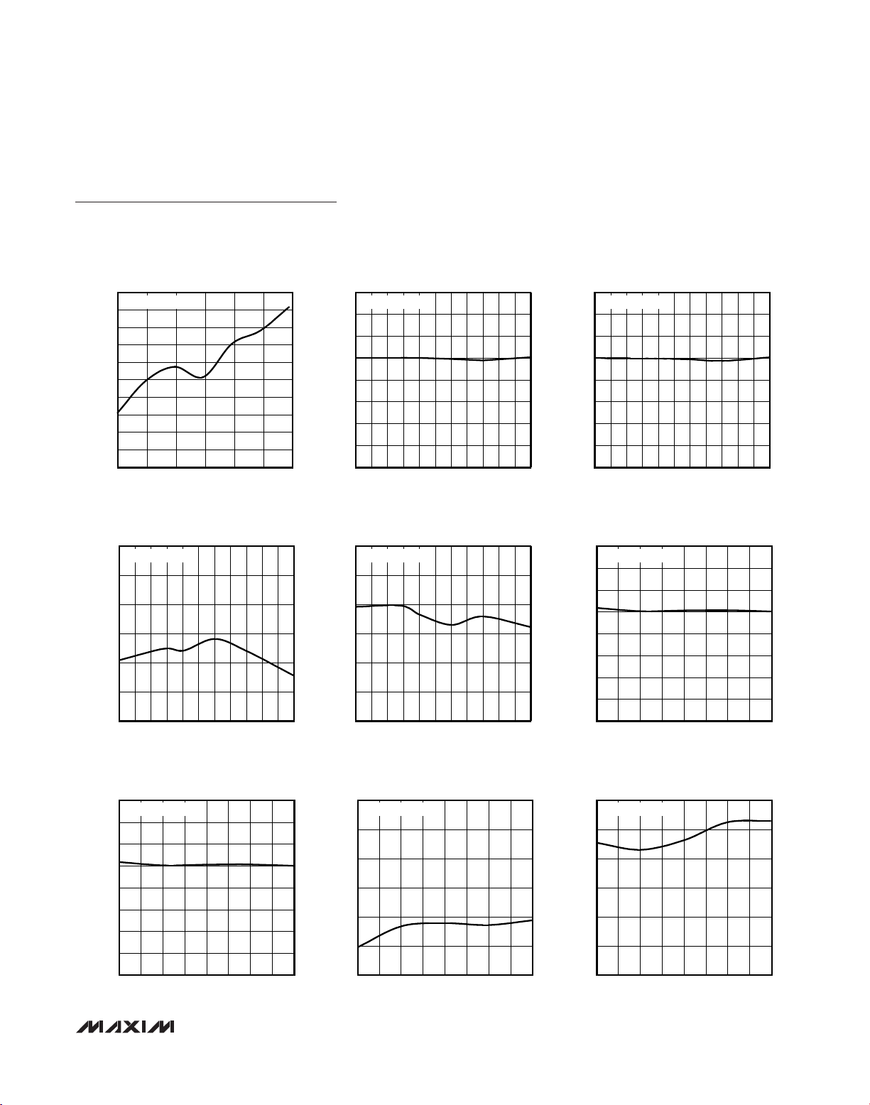
Typical Operating Characteristics (continued)
(V
AVDD
= 1.8V, V
OVDD
= 1.8V, V
CVDD
= 3.3V, V
GND
= 0V, internal reference, differential input at -0.5dBFS, fIN= 5.3MHz, f
CLK
= 65MHz
(50% duty cycle), V
DT
= 0V, C
LOAD
= 10pF, TA= +25°C, unless otherwise noted.)
SPURIOUS-FREE DYNAMIC RANGE
vs. ANALOG INPUT POWER
95
fIN = 5.304814MHz
90
85
80
75
70
SFDR (dBc)
65
60
55
50
45
-30 0
ANALOG INPUT POWER (dBFS
TOTAL HARMONIC DISTORTION
vs. SAMPLING RATE
-75
fIN = 5.304814MHz
-80
-85
-90
THD (dBc)
-95
-100
-105
10 20 25 3015 35 40 5550 6045 65
f
(MHz)
CLK
SIGNAL-TO-NOISE PLUS DISTORTION
vs. DUTY CYCLE
73
fIN = 5.304814MHz
72
71
70
69
SINAD (dB)
68
67
66
65
30 70
DUTY CYCLE (%)
MAX1438 toc13
-5-10-25 -20 -15
MAX1438 toc16
MAX1438 toc19
60 655540 4535 50
SIGNAL-TO-NOISE RATIO
vs. SAMPLING RATE
73
fIN = 5.304814MHz
72
71
70
69
SNR (dB)
68
67
66
65
10 20 25 3015 35 40 5550 6045 65
f
SPURIOUS-FREE DYNAMIC RANGE
vs. SAMPLING RATE
105
fIN = 5.304814MHz
100
95
90
SFDR (dBc)
85
80
75
10 20 25 3015 35 40 5550 6045 65
f
CLK
TOTAL HARMONIC DISTORTION
vs. DUTY CYCLE
-75
fIN = 5.304814MHz
-80
-85
-90
THD (dBc)
-95
-100
-105
30 70
DUTY CYCLE (%)
(MHz
(MHz)
SIGNAL-TO-NOISE PLUS DISTORTION
vs. SAMPLING RATE
73
fIN = 5.304814MHz
72
MAX1438 toc14
71
70
69
SINAD (dB)
68
67
66
65
10 20 25 3015 35 40 5550 6045 65
f
(MHz
SIGNAL-TO-NOISE RATIO
vs. DUTY CYCLE
73
fIN = 5.304814MHz
72
MAX1438 toc17
71
70
69
SNR (dB)
68
67
66
65
30 70
DUTY CYCLE (%)
60 655540 4535 50
SPURIOUS-FREE DYNAMIC RANGE
vs. DUTY CYCLE
100
fIN = 5.304814MHz
95
MAX1438 toc20
90
85
SFDR (dBc)
80
75
70
60 655540 4535 50
30 70
DUTY CYCLE (%)
60 655540 4535 50
MAX1438 toc15
MAX1438 toc18
MAX1438 toc21
Page 8

MAX1438
Octal, 12-Bit, 65Msps, 1.8V ADC
with Serial LVDS Outputs
8 _______________________________________________________________________________________
Typical Operating Characteristics (continued)
(V
AVDD
= 1.8V, V
OVDD
= 1.8V, V
CVDD
= 3.3V, V
GND
= 0V, internal reference, differential input at -0.5dBFS, fIN= 5.3MHz, f
CLK
= 65MHz
(50% duty cycle), V
DT
= 0V, C
LOAD
= 10pF, TA= +25°C, unless otherwise noted.)
SIGNAL-TO-NOISE RATIO
vs. TEMPERATURE
TEMPERATURE (°C)
SNR (dB)
-15 10 6035
68
70
69
67
66
72
71
73
65
-40 85
MAX1438 toc22
f
CLK
= 65MHz
f
IN
= 19.8MHz
4096-POINT DATA RECORD
SIGNAL-TO-NOISE PLUS DISTORTION
vs. TEMPERATURE
TEMPERATURE (°C)
SINAD (dB)
-15 10 6035
68
70
69
67
66
72
71
73
65
-40 85
MAX1438 toc23
f
CLK
= 65MHz
f
IN
= 19.8MHz
4096-POINT DATA RECORD
TOTAL HARMONIC DISTORTION
vs. TEMPERATURE
TEMPERATURE (°C)
THD (dBc)
-15 10 6035
-90
-88
-89
-91
-94
-92
-93
-86
-87
-85
-95
-40 85
MAX1438 toc24
f
CLK
= 65MHz
f
IN
= 19.8MHz
4096-POINT DATA RECORD
SPURIOUS-FREE DYNAMIC RANGE
vs. TEMPERATURE
TEMPERATURE (°C)
SFDR (dBc)
-15 10 6035
90
92
91
89
86
88
87
94
93
95
85
-40 85
MAX1438 toc25
f
CLK
= 65MHz
f
IN
= 19.8MHz
4096-POINT DATA RECORD
340
360
350
390
380
370
400
410
420
430
010155 20253035404550556065
SUPPLY CURRENT
vs. SAMPLING RATE (AVDD)
MAX1438 toc26
f
CLK
(MHz)
I
AVDD
(mA)
60
90
85
80
75
70
65
010155 20253035404550556065
SUPPLY CURRENT
vs. SAMPLING RATE (OVDD)
MAX1438 toc27
f
CLK
(MHz)
I
OVDD
(mA)
OFFSET ERROR
vs. TEMPERATURE
TEMPERATURE (°C)
OFFSET ERROR (%FS)
-15 10 6035
0.05
0.04
0.03
0.02
0.01
0
-0.01
-0.02
-0.03
-0.04
-0.05
-40 85
MAX1438 toc28
-1.2
-0.8
-1.0
-0.4
-0.6
-0.2
0
-40 85
GAIN ERROR
vs. TEMPERATURE
MAX1438 toc29
TEMPERATURE (°C)
GAIN ERROR (%FS)
10-15 35 60
INTEGRAL NONLINEARITY
vs. DIGITAL OUTPUT CODE
MAX1438 toc30
DIGITAL OUTPUT CODE
INL (LSB)
1024 30722048512 2560 35841536
0.3
0.2
0.1
0
-0.1
-0.2
-0.3
0 4096
Page 9
MAX1438
Octal, 12-Bit, 65Msps, 1.8V ADC
with Serial LVDS Outputs
_______________________________________________________________________________________
9
Typical Operating Characteristics (continued)
(V
AVDD
= 1.8V, V
OVDD
= 1.8V, V
CVDD
= 3.3V, V
GND
= 0V, internal reference, differential input at -0.5dBFS, fIN= 5.3MHz, f
CLK
= 65MHz
(50% duty cycle), V
DT
= 0V, C
LOAD
= 10pF, TA= +25°C, unless otherwise noted.)
DIFFERENTIAL NONLINEARITY
vs. DIGITAL OUTPUT CODE
0.3
0.2
0.1
0
DNL (LSB)
-0.1
-0.2
-0.3
0 4096
1024 30722048512 2560 35841536
DIGITAL OUTPUT CODE
INTERNAL REFERENCE VOLTAGE
vs. REFERENCE LOAD CURRENT
1.40
1.35
1.30
1.25
(V)
1.20
REFIO
V
1.15
1.10
1.05
1.00
-350 350
-250 -150 50 250150-50
I
(µA)
REFIO
MAX1438 toc31
MAX1438 toc34
INTERNAL REFERENCE VOLTAGE
vs. SUPPLY VOLTAGE
1.2510
V
= V
AVDD
OVDD
1.2500
(V)
1.2490
REFIO
V
1.2480
1.2470
1.7 2.1
SUPPLY VOLTAGE (V)
CMOUT VOLTAGE
vs. SUPPLY VOLTAGE
0.770
V
= V
AVDD
OVDD
0.768
0.766
(V)
CMOUT
V
0.764
0.762
0.760
1.7 2.1
SUPPLY VOLTAGE (V)
CMOUT VOLTAGE
vs. LOAD CURRENT
1.8
1.6
1.4
1.2
(V)
1.0
0.8
CMOUT
V
0.6
0.4
0.2
0
0 2000
I
CMOUT
(µA)
INTERNAL REFERENCE VOLTAGE
V
V
AVDD
AVDD
= V
= V
OVDD
OVDD
vs. TEMPERATURE
MAX1438 toc33
603510-15
TEMPERATURE (°C)
CMOUT VOLTAGE
vs. TEMPERATURE
MAX1438 toc36
603510-15
TEMPERATURE (°C)
1.26
MAX1438 toc32
1.25
(V)
1.24
REFIO
V
1.23
1.22
2.01.91.8
MAX1438 toc35
2.01.91.8
MAX1438 toc37
15001000500
-40 85
0.770
0.768
0.766
(V)
CMOUT
0.764
V
0.762
0.760
-40 85
Page 10

MAX1438
Octal, 12-Bit, 65Msps, 1.8V ADC
with Serial LVDS Outputs
10 ______________________________________________________________________________________
Pin Description
PIN NAME FUNCTION
1, 4, 7, 10, 16, 19, 22,
25, 26, 27, 30, 36, 89,
92, 96, 99, 100
2 IN1P Channel 1 Positive Analog Input
11, 12, 13, 15, 37–42,
14, 31, 50, 51, 70,
43, 46, 49, 54, 57, 60,
63, 64, 67, 71, 74, 77
3 IN1N Channel 1 Negative Analog Input
5 IN2P Channel 2 Positive Analog Input
6 IN2N Channel 2 Negative Analog Input
8 IN3P Channel 3 Positive Analog Input
9 IN3N Channel 3 Negative Analog Input
86, 87, 88
75, 76
17 IN4P Channel 4 Positive Analog Input
18 IN4N Channel 4 Negative Analog Input
20 IN5P Channel 5 Positive Analog Input
21 IN5N Channel 5 Negative Analog Input
23 IN6P Channel 6 Positive Analog Input
24 IN6N Channel 6 Negative Analog Input
28 IN7P Channel 7 Positive Analog Input
29 IN7N Channel 7 Negative Analog Input
32 DT
33 SLVS/LVDS
34 CVDD
35 CLK Single-Ended CMOS Clock Input
44 OUT7N Channel 7 Negative LVDS/SLVS Output
45 OUT7P Channel 7 Positive LVDS/SLVS Output
47 OUT6N Channel 6 Negative LVDS/SLVS Output
48 OUT6P Channel 6 Positive LVDS/SLVS Output
52 OUT5N Channel 5 Negative LVDS/SLVS Output
53 OUT5P Channel 5 Positive LVDS/SLVS Output
55 OUT4N Channel 4 Negative LVDS/SLVS Output
56 OUT4P Channel 4 Positive LVDS/SLVS Output
GND Ground. Connect all GND pins to the same potential.
Analog Power Input. Connect AVDD to a +1.7V to +1.9V power supply. Bypass AVDD to GND
AVDD
N.C. No Connection. Not internally connected.
OVDD
with a 0.1µF capacitor as close as possible to the device. Bypass the AVDD power plane to
the GND plane with a bulk ≥ 2.2µF capacitor. Connect all AVDD pins to the same potential.
Double-Termination Select. Drive DT high to select the internal 100Ω termination between the
differential output pairs. Drive DT low to select no output termination.
Differential Output-Signal Format-Select Input. Drive SLVS/LVDS high to select SLVS outputs.
Drive SLVS/LVDS low to select LVDS outputs.
Clock Power Input. Connect CVDD to a +1.7V to +3.6V power supply. Bypass CVDD to GND
with a 0.1µF capacitor in parallel with a ≥ 2.2µF capacitor. Install the bypass capacitors as
close as possible to the device.
O utp ut- D r i ver P ow er Inp ut. C onnect O V D D to a + 1.7V to + 1.9V p ow er sup p l y. Byp ass O V D D to
G N D w i th a 0.1µF cap aci tor as cl ose as p ossi b l e to the d evi ce. Byp ass the O V D D p ow er p l ane
to the G N D p l ane w i th a b ul k ≥ 2.2µF cap aci tor . C onnect al l O V D D p i ns to the sam e p otenti al .
Page 11

MAX1438
Octal, 12-Bit, 65Msps, 1.8V ADC
with Serial LVDS Outputs
______________________________________________________________________________________ 11
Pin Description (continued)
PIN NAME FUNCTION
58 FRAMEN
59 FRAMEP
61 CLKOUTN Negative LVDS/SLVS Serial Clock Output
62 CLKOUTP Positive LVDS/SLVS Serial Clock Output
65 OUT3N Channel 3 Negative LVDS/SLVS Output
66 OUT3P Channel 3 Positive LVDS/SLVS Output
68 OUT2N Channel 2 Negative LVDS/SLVS Output
69 OUT2P Channel 2 Positive LVDS/SLVS Output
72 OUT1N Channel 1 Negative LVDS/SLVS Output
73 OUT1P Channel 1 Positive LVDS/SLVS Output
78 OUT0N Channel 0 Negative LVDS/SLVS Output
79 OUT0P Channel 0 Positive LVDS/SLVS Output
80 LVDSTEST
81 PD
82 PLL3 PLL Control Input 3. See Table 1 for details.
83 PLL2 PLL Control Input 2. See Table 1 for details.
84 PLL1 PLL Control Input 1. See Table 1 for details.
85 T/B
90 REFN
91 REFP
93 REFIO
94 REFADJ
95 CMOUT
97 IN0P Channel 0 Positive Analog Input
98 IN0N Channel 0 Negative Analog Input
— EP Exposed Pad. EP is internally connected to GND. Connect EP to GND.
Negative Frame-Alignment LVDS/SLVS Output. A rising edge on the differential FRAME
output aligns to a valid D0 in the output data stream.
Positive Frame-Alignment LVDS/SLVS Output. A rising edge on the differential FRAME output
aligns to a valid D0 in the output data stream.
LVDS Test Pattern Enable. Drive LVDSTEST high to enable the output test pattern (0000 1011
1101 MSB → LSB). As with the analog conversion results, the test pattern data is output LSB
first. Drive LVDSTEST low for normal operation.
Power-Down Input. Drive PD high to power down all channels and reference. Drive PD low for
normal operation.
Output Format-Select Input. Drive T/B high to select binary output format. Drive T/B low to
select two’s-complement output format.
N eg ati ve Refer ence Byp ass O utp ut. C onnect a ≥ 1µF ( 10µF typ ) cap aci tor b etw een RE FP and
RE FN , and connect a ≥ 1µF ( 10µF typ ) cap aci tor b etw een RE FN and GN D . Pla c e t h e
c a p a c it o r s a s c lo s e as p o s s ib le t o t h e de v i c e on t h e sa m e si d e of t h e PC B .
Positive Reference Bypass Output. Connect a ≥ 1µF (10µF typ) capacitor between REFP and
REFN, and connect a ≥ 1µF (10µF typ) capacitor between REFP and GND. Place the
capacitors as close as possible to the device on the same side of the PCB.
Reference Input/Output. For internal reference operation (REFADJ = GND), the reference
output voltage is 1.24V. For external reference operation (REFADJ = AVDD), apply a stable
reference voltage at REFIO. Bypass to GND with ≥ 0.1µF.
Internal/External Reference-Mode-Select and Reference Adjust Input. For internal reference
mode, connect REFADJ directly to GND. For external reference mode, connect REFADJ
directly to AVDD. For reference-adjust mode, see the Full-Scale Range Adjustments Using the
Internal Reference section.
Common-Mode Reference Voltage Output. CMOUT outputs the input common-mode voltage
for DC-coupled applications. Bypass CMOUT to GND with ≥ 0.1µF capacitor.
Page 12

MAX1438
Detailed Description
The MAX1438 ADC features fully differential inputs, a
pipelined architecture, and digital error correction for
high-speed signal conversion. The ADC pipeline architecture moves the samples taken at the inputs through
the pipeline stages every half clock cycle. The converted digital results are serialized and sent through the
LVDS/SLVS output drivers. The total clock-cycle latency
from input to output is 6.5 clock cycles.
The MAX1438 offers eight separate fully differential channels with synchronized inputs and outputs. Configure the
outputs for binary or two’s complement with the T/B digital
input. Global power-down minimizes power consumption.
Input Circuit
Figure 1 displays a simplified diagram of the input T/H
circuits. In track mode, switches S1, S2a, S2b, S4a, S4b,
S5a, and S5b are closed. The fully differential circuits
sample the input signals onto the two capacitors (C2a
and C2b) through switches S4a and S4b. S2a and S2b
set the common mode for the operational transconductance amplifier (OTA), and open simultaneously with S1,
sampling the input waveform. Switches S4a, S4b, S5a,
and S5b are then opened before switches S3a and S3b
connect capacitors C1a and C1b to the output of the
amplifier and switch S4c is closed. The resulting differential voltages are held on capacitors C2a and C2b. The
amplifiers charge capacitors C1a and C1b to the same
values originally held on C2a and C2b. These values are
Octal, 12-Bit, 65Msps, 1.8V ADC
with Serial LVDS Outputs
12 ______________________________________________________________________________________
Functional Diagram
CMOUT
IN0P
IN0N
IN1P
IN1N
IN7P
IN7N
CLK
CLOCK
CIRCUITRY
REFADJ REFIO REFP REFN
REFERENCE SYSTEM
ICMV*
T/H
T/H
T/H
12-BIT
PIPELINE
ADC
12-BIT
PIPELINE
ADC
12-BIT
PIPELINE
ADC
PLL
6x
PD
POWER
CONTROL
OVDDAVDD
MAX1438
12:1
SERIALIZER
12:1
SERIALIZER
12:1
SERIALIZER
DT
OUTPUT
CONTROL
LVDS/SLVS
OUTPUT
DRIVERS
SLVS/LVDS
LVDSTEST
T/B
OUT0P
OUT0N
OUT1P
OUT1N
OUT7P
OUT7N
FRAMEP
FRAMEN
CLKOUTP
CLKOUTN
CVDD
*ICMV = INPUT COMMON-MODE VOLTAGE (INTERNALLY GENERATED).
PLL3PLL1 PLL2
GND
Page 13

then presented to the first-stage quantizers and isolate
the pipelines from the fast-changing inputs. Analog
inputs, IN_P to IN_N, are driven differentially. For differential inputs, balance the input impedance of IN_P and
IN_N for optimum performance.
Reference Configurations (REFIO,
REFADJ, REFP, and REFN)
The MAX1438 provides an internal 1.24V bandgap reference or can be driven with an external reference voltage. The full-scale analog differential input range is
±FSR. FSR (full-scale range) is given by the following
equation:
where V
REFIO
is the voltage at REFIO, generated inter-
nally or externally. For a V
REFIO
= 1.24V, the full-scale
input range is ±700mV (1.4V
P-P
).
Internal Reference Mode
Connect REFADJ to GND to use the internal bandgap
reference directly. The internal bandgap reference generates V
REFIO
to be 1.24V with a 120ppm/°C temperature coefficient in internal reference mode. Connect an
external ≥ 0.1µF bypass capacitor from REFIO to GND
for stability. REFIO sources up to 200µA and sinks up
to 200µA for external circuits, and REFIO has a
75mV/mA load regulation. REFIO has > 1MΩ to GND
when the MAX1438 is in power-down mode. The internal reference circuit requires 100ms (C
REFP
to GND =
C
REFN
to GND = 1µF) to power up and settle when
power is applied to the MAX1438 or when PD transitions from high to low.
To compensate for gain errors or to decrease or
increase the ADC’s FSR, add an external resistor
between REFADJ and GND or REFADJ and REFIO.
This adjusts the internal reference value of the
MAX1438 by up to ±5% of its nominal value. See the
Full-Scale Range Adjustments Using the Internal
Reference
section.
MAX1438
Octal, 12-Bit, 65Msps, 1.8V ADC
with Serial LVDS Outputs
______________________________________________________________________________________________________ 13
Figure 1. Internal Input Circuit
SWITCHES SHOWN IN TRACK MODE
INTERNALLY
INTERNAL
COMMON-MODE
BIAS*
INTERNAL
BIAS*
GENERATED
COMMON-MODE
LEVEL*
AVDD
IN_P
IN_N
GND
*NOT EXTERNALLY ACCESSIBLE
INTERNAL
COMMON-MODE
BIAS*
MAX1438
S4a
S4c S1
S4b
C2a
C2b
V
×(. )
=
0 700
FSR
REFIO
V
.
124
S2a
S2b
INTERNAL
BIAS*
OTA
C1a
C1b
S5a
S5b
INTERNALLY
GENERATED
COMMON-MODE
LEVEL*
S3a
OUT
OUT
S3b
Page 14

MAX1438
Connect ≥ 1µF (10µF typ) capacitors to GND from
REFP and REFN and a ≥ 1µF (10µF typ) capacitor
between REFP and REFN as close to the device as
possible on the same side of the PC board.
External Reference Mode
The external reference mode allows for more control
over the MAX1438 reference voltage and allows multiple converters to use a common reference. Connect
REFADJ to AVDD to disable the internal reference.
Apply a stable 1.18V to 1.30V source at REFIO. Bypass
REFIO to GND with a ≥ 0.1µF capacitor. The REFIO
input impedance is > 1MΩ.
Clock Input (CLK)
The MAX1438 accepts a CMOS-compatible clock signal with a wide 20% to 80% input clock duty cycle.
Drive CLK with an external single-ended clock signal.
Figure 2 shows the simplified clock input diagram.
Low clock jitter is required for the specified SNR performance of the MAX1438. Analog input sampling occurs
on the rising edge of CLK, requiring this edge to provide the lowest possible jitter. Jitter limits the maximum
SNR performance of any ADC according to the following relationship:
where fINrepresents the analog input frequency and t
J
is the total system clock jitter.
PLL Inputs (PLL1, PLL2, PLL3)
The MAX1438 features a PLL that generates an output
clock signal with 6 times the frequency of the input
clock. The output clock signal is used to clock data out
of the MAX1438 (see the
System Timing Requirements
section). Set the PLL1, PLL2, and PLL3 bits according
to the input clock range provided in Table 1.
System Timing Requirements
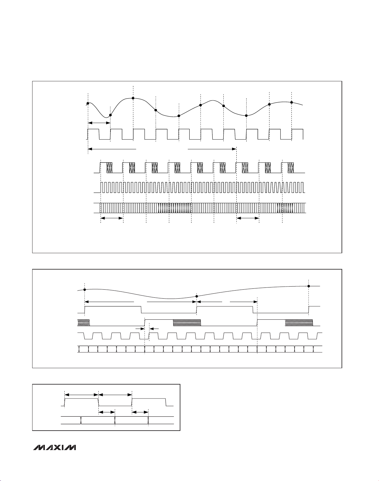
Figure 3 shows the relationship between the analog
inputs, input clock, frame-alignment output, serial-clock
output, and serial-data output. The differential analog
input (IN_P and IN_N) is sampled on the rising edge of
the CLK signal and the resulting data appears at the
digital outputs 6.5 clock cycles later. Figure 4 provides
a detailed, two-conversion timing diagram of the relationship between the inputs and the outputs.
Clock Output (CLKOUTP, CLKOUTN)
The MAX1438 provides a differential clock output that
consists of CLKOUTP and CLKOUTN. As shown in Figure
4, the serial output data is clocked out of the MAX1438 on
both edges of the clock output. The frequency of the output clock is 6 times the frequency of CLK.
Frame-Alignment Output (FRAMEP, FRAMEN)
The MAX1438 provides a differential frame-alignment
signal that consists of FRAMEP and FRAMEN. As
shown in Figure 4, the rising edge of the frame-alignment signal corresponds to the first bit (D0) of the 12bit serial data stream. The frequency of the framealignment signal is identical to the frequency of the
input clock.
Serial Output Data (OUT_P, OUT_N)
The MAX1438 provides its conversion results through
individual differential outputs consisting of OUT_P and
OUT_N. The results are valid 6.5 input clock cycles
after the sample is taken. As shown in Figure 3, the output data is clocked out on both edges of the output
clock, LSB (D0) first. Figure 5 provides the detailed serial-output timing diagram.
Octal, 12-Bit, 65Msps, 1.8V ADC
with Serial LVDS Outputs
14 ______________________________________________________________________________________
Figure 2. Clock Input Circuitry
Table 1. PLL1, PLL2, and PLL3
Configuration Table
SNR
=×
20
log
⎛
⎜
⎝
1
×× ×
2
π
⎞
⎟
ft
⎠
IN J
AVDD
CVDD
CLK
GND
MAX1438
DUTY-CYCLE
EQUALIZER
INPUT CLOCK RANGE
PLL1 PLL2 PLL3
0 0 0 45.0 65.0
0 0 1 32.5 45.0
0 1 0 22.5 32.5
0 1 1 16.3 22.5
1 0 0 11.3 16.3
1 0 1 8.1 11.3
1 1 0 5.6 8.1
1 1 1 4.0 5.6
(MHz)
MIN MAX
Page 15
MAX1438
Octal, 12-Bit, 65Msps, 1.8V ADC
with Serial LVDS Outputs
______________________________________________________________________________________ 15
Figure 3. Global Timing Diagram
Figure 4. Detailed Two-Conversion Timing Diagram
Figure 5. Serialized-Output Detailed Timing Diagram
N
(V
-
IN_P
)
V
IN_N
CLK
-
(V
FRAMEP
)*
V
FRAMEN
(V
-
CLKOUTP
)
V
CLKOUTN
(V
-
OUT_P
)
V
OUT_N
*DUTY CYCLE VARIES DEPENDING ON INPUT CLOCK FREQUENCY.
t
SAMPLE
N + 1
DATA FOR
OUTPUT
SAMPLE
N - 6
N + 2
N + 3
6.5 CLOCK-CYCLE DATA LATENCY
N + 4
N + 5
N + 6
N + 7
OUTPUT
DATA FOR
SAMPLE N
N + 8
N + 9
N
(V
- V
)
IN_P
IN_N
t
SAMPLE
CLK
-
(V
FRAMEP
)*
V
FRAMEN
(V
-
CLKOUTP
)
V
CLKOUTN
-
(V
OUT_P
D5
N-7D6N-7D7N-7D8N-7D9N-7
)
V
OUT_N
*DUTY CYCLE DEPENDS ON INPUT CLOCK FREQUENCY.
D10
N-7
t
D11
N-7D0N-6D1N-6D2N-6D3N-6D4N-6D5N-6D6N-6D7N-6D8N-6D9N-6
(V
CLKOUTP
V
(V
CLKOUTN
OUT_P
V
OUT_N
t
CH
)
-
D0 D1 D2 D3
)
t
CL
t
OD
t
OD
N + 2
N + 1
t
SF
CF
D10
D11
N-6
N-6D0N-5D1N-5D2N-5D3N-5D4N-5D5N-5D6N-5
Page 16
MAX1438
Output Data Format (T/B) Transfer Functions
The MAX1438 output data format is either offset binary
or two’s complement, depending on the logic-input T/B.
With T/B low, the output data format is two’s complement. With T/B high, the output data format is offset
binary. The following equations, Table 2, and Figures 6
and 7 define the relationship between the digital output
and the analog input. For two’s complement (T/B = 0):
and for offset binary (T/B = 1):
where CODE
10
is the decimal equivalent of the digital
output code as shown in Table 2.
Keep the capacitive load on the MAX1438 digital outputs as low as possible.
Octal, 12-Bit, 65Msps, 1.8V ADC
with Serial LVDS Outputs
16 ______________________________________________________________________________________
)
(
)
Table 2. Output Code Table (V
REFIO
= 1.24V)
Figure 6. Two’s-Complement Transfer Function (T/B = 0)
Figure 7. Binary Transfer Function (T/B = 1)
TWO’S-COMPLEMENT DIGITAL OUTPUT CODE
BINARY
D11 → D0
0111 1111 1111 0x7FF +2047 1111 1111 1111 0xFFF +4095 +699.66
0111 1111 1110 0x7FE +2046 1111 1111 1110 0xFFE +4094 +699.32
0000 0000 0001 0x001 +1 1000 0000 0001 0x801 +2049 +0.34
0000 0000 0000 0x000 0 1000 0000 0000 0x800 +2048 0
1111 1111 1111 0xFFF -1 0111 1111 1111 0x7FF +2047 -0.34
1000 0000 0001 0x801 -2047 0000 0000 0001 0x001 +1 -699.66
1000 0000 0000 0x800 -2048 0000 0000 0000 0x000 0 -700.00
0x7FF
0x7FE
0x7FD
(T/B = 0)
HEXADECIMAL
EQUIVALENT
OF D11 → D0
2 x FSR
1 LSB =
4096
FSR FSR
FSR = 700mV x
DECIMAL
EQUIVALENT
OF D11 → D0
V
REFIO
1.24V
OFFSET BINARY DIGITAL OUTPUT CODE
BINARY
D11 → D0
(T/B = 1)
HEXADECIMAL
EQUIVALENT
OF D11 → D0
1 LSB =
0xFFF
0xFFE
0xFFD
DECIMAL
EQUIVALENT
OF D11 → D0
2 x FSR
4096
FSR = 700mV x
FSR FSR
V
V
IN_P
REFIO
1.24V
V
REFIO
- VIN_N (mV
= 1.24V
0x001
0x000
0xFFF
0x803
0x802
0x801
TWO'S-COMPLEMENT OUTPUT CODE (LSB)
0x800
-2045 +2047+2045-1 0 +1-2047
DIFFERENTIAL INPUT VOLTAGE (LSB)
0x801
0x800
0x7FF
0x003
0x002
OFFSET BINARY OUTPUT CODE (LSB)
0x800
0x000
-2045 +2047+2045-1 0 +1-2047
DIFFERENTIAL INPUT VOLTAGE (LSB)
V V FSR
−=××
IN P IN N__
CODE
CODE
V V FSR
−=××2
IN P IN N__
10
4096
10
4096
−22048
Page 17
LVDS and SLVS Signals (SLVS/
LVDS
)
Drive SLVS/LVDS low for LVDS or drive SLVS/LVDS high
for SLVS levels at the MAX1438 outputs (OUT_P, OUT_N,
CLKOUTP, CLKOUTN, FRAMEP, and FRAMEN). For
SLVS levels, enable double-termination by driving DT
high. See the
Electrical Characteristics
table for LVDS
and SLVS output voltage levels.
LVDS Test Pattern (LVDSTEST)
Drive LVDSTEST high to enable the output test pattern
on all LVDS or SLVS output channels. The output test
pattern is 0000 1011 1101. Drive LVDSTEST low for
normal operation (test pattern disabled).
Common-Mode Output (CMOUT)
CMOUT provides a common-mode reference for DCcoupled analog inputs. If the input is DC-coupled,
match the output common-mode voltage of the circuit
driving the MAX1438 to the output voltage at V
CMOUT
to within ±50mV. It is recommended that the output
common-mode voltage of the driving circuit be derived
from CMOUT.
Double-Termination (DT)
The MAX1438 offers an optional, internal 100Ω termination
between the differential output pairs (OUT_P and OUT_N,
CLKOUTP and CLKOUTN, FRAMEP and FRAMEN).
In addition to the termination at the end of the line, a
second termination directly at the outputs helps eliminate
unwanted reflections down the line. This feature is useful
in applications where trace lengths are long (>5in) or with
mismatched impedance. Drive DT high to select doubletermination, or drive DT low to disconnect the internal termination resistor (single-termination). Selecting
double-termination increases the OVDD supply current
(see Figure 8).
Power-Down Mode (PD)
The MAX1438 offers a power-down mode to efficiently
use power by transitioning to a low-power state when
conversions are not required.
PD controls the power-down mode of all channels and
the internal reference circuitry. Drive PD high to enable
power-down. In power-down mode, the output impedance of all of the LVDS/SLVS outputs is approximately
342Ω, if DT is low. The output impedance of the differential LVDS/SLVS outputs is 100Ω when DT is high. See the
Electrical Characteristics
table for typical supply currents
during power-down. The following list shows the state of
the analog inputs and digital outputs in power-down
mode:
• IN_P, IN_N analog inputs are disconnected from
the internal input amplifier
• REFIO has > 1MΩ to GND
• OUT_P, OUT_N, CLKOUTP, CLKOUTN, FRAMEP,
and FRAMEN have approximately 342Ω between
the output pairs when DT is low. When DT is high,
the differential output pairs have 100Ω between
each pair.
When operating from the internal reference, the wakeup time from power-down is typically 100ms (C
REFP
to
GND = C
REFN
to GND = 1µF). When using an external
reference, the wake-up time is dependent on the external reference drivers.
Applications Information
Full-Scale Range Adjustments
Using the Internal Reference
The MAX1438 supports a full-scale adjustment range of
10% (±5%). To decrease the full-scale range, add a
25kΩ to 250kΩ external resistor or potentiometer (R
ADJ
)
between REFADJ and GND. To increase the full-scale
range, add a 25kΩ to 250kΩ resistor between REFADJ
and REFIO. Figure 9 shows the two possible configurations.
The following equations provide the relationship between
R
ADJ
and the change in the analog full-scale range:
for R
ADJ
connected between REFADJ and REFIO, and:
MAX1438
Octal, 12-Bit, 65Msps, 1.8V ADC
with Serial LVDS Outputs
______________________________________________________________________________________________________ 17
Figure 8. Double-Termination
DT
OUT_P/
CLKOUTP/
FRAMEP
Ω
100
OUT_N/
MAX1438
SWITCHES ARE CLOSED WHEN DT IS HIGH.
SWITCHES ARE OPEN WHEN DT IS LOW.
CLKOUTN/
FRAMEN
Ω
= 50
Z
0
Ω
100
Ω
Z
= 50
0
⎛
⎜
⎝
125.. Ω
07 1
FSR V
=+
R
k
ADJ
⎞
⎟
⎠
Page 18
MAX1438
for R
ADJ
connected between REFADJ and GND.
Using Transformer Coupling
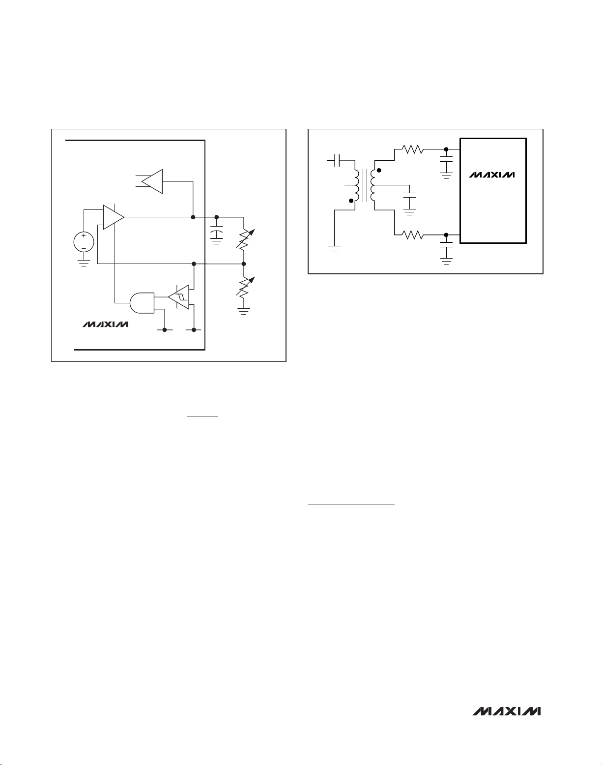
An RF transformer (Figure 10) provides an excellent
solution to convert a single-ended input source signal
to a fully differential signal. The MAX1438 input common-mode voltage is internally biased to 0.76V (typ)
with f
CLK
= 65MHz. Although a 1:1 transformer is
shown, a step-up transformer can be selected to
reduce the drive requirements. A reduced signal swing
from the input driver, such as an op amp, can also
improve the overall distortion.
Grounding, Bypassing, and Board Layout
The MAX1438 requires high-speed board layout design
techniques. Refer to the MAX1434/MAX1436/MAX1437/
MAX1438 EV kit data sheet for a board layout reference. Locate all bypass capacitors as close to the
device as possible, preferably on the same side as the
ADC, using surface-mount devices for minimum inductance. Bypass AVDD to GND with a 0.1µF ceramic
capacitor in parallel with a 0.1µF ceramic capacitor.
Bypass OVDD to GND with a 0.1µF ceramic capacitor
in parallel with a ≥ 2.2µF ceramic capacitor. Bypass
CVDD to GND with a 0.1µF ceramic capacitor in parallel with a ≥ 2.2µF ceramic capacitor.
Multilayer boards with ample ground and power planes
produce the highest level of signal integrity. Connect
MAX1438 ground pins and the exposed pad to the
same ground plane. The MAX1438 relies on the
exposed-pad connection for a low-inductance ground
connection. Isolate the ground plane from any noisy
digital system ground planes.
Route high-speed digital signal traces away from the
sensitive analog traces. Keep all signal lines short and
free of 90° turns.
Ensure that the differential analog input network layout is
symmetric and that all parasitics are balanced equally.
Refer to the MAX1434/MAX1436/MAX1437/MAX1438 EV
kit data sheet for an example of symmetric input layout.
Parameter Definitions
Integral Nonlinearity (INL)
Integral nonlinearity is the deviation of the values on an
actual transfer function from a straight line. For the
MAX1438, this straight line is between the end points of
the transfer function, once offset and gain errors have
been nullified. INL deviations are measured at every
step and the worst-case deviation is reported in the
Electrical Characteristics
table.
Differential Nonlinearity (DNL)
Differential nonlinearity is the difference between an
actual step width and the ideal value of 1 LSB. A DNL
error specification of less than 1 LSB guarantees no
missing codes and a monotonic transfer function. For
the MAX1438, DNL deviations are measured at every
step and the worst-case deviation is reported in the
Electrical Characteristics
table.
Octal, 12-Bit, 65Msps, 1.8V ADC
with Serial LVDS Outputs
18 ______________________________________________________________________________________
Figure 9. Circuit Suggestions to Adjust the ADC’s Full-Scale
Range
Figure 10. Transformer-Coupled Input Drive
ADC FULL-SCALE = REFT - REFB
REFERENCE-
SCALING
REFT
REFB
REFERENCE
BUFFER
1V
CONTROL LINE TO
DISABLE REFERENCE
BUFFER
MAX1438
FSR V
G
AVDD AVDD/2
=
07 1
AMPLIFIER
REFADJ
⎛
−
⎜
⎝
REFIO
k
125.. Ω
R
ADJ
⎞
⎟
⎠
0.1µF
25kΩ
250kΩ
25kΩ
250kΩ
0.1µF
IN
1
2
N.C.
3
MINI-CIRCUITS
T1
ADT1-1WT
V
10Ω
6
5
4
39pF
0.1µF
10Ω
39pF
IN_P
MAX1438
IN_N
Page 19
Offset Error
Offset error is a figure of merit that indicates how well
the actual transfer function matches the ideal transfer
function at a single point. For the MAX1438, the ideal
midscale digital output transition occurs when there is
-1/2 LSBs across the analog inputs (Figures 6 and 7).
Bipolar offset error is the amount of deviation between
the measured midscale transition point and the ideal
midscale transition point.
Gain Error
Gain error is a figure of merit that indicates how well the
slope of the actual transfer function matches the slope
of the ideal transfer function. For the MAX1438 the gain
error is the difference of the measured full-scale and
zero-scale transition points minus the difference of the
ideal full-scale and zero-scale transition points.
For the bipolar devices (MAX1438), the full-scale transition point is from 0x7FE to 0x7FF for two’s-complement
output format (0xFFE to 0xFFF for offset binary) and the
zero-scale transition point is from 0x800 to 0x801 for
two’s complement (0x000 to 0x001 for offset binary).
Crosstalk
Crosstalk indicates how well each analog input is isolated
from the others. For the MAX1438, a 5.3MHz, -0.5dBFS
analog signal is applied to one channel while a 19.3MHz,
-0.5dBFS analog signal is applied to another channel. An
FFT is taken on the channel with the 5.3MHz analog signal. From this FFT, the crosstalk is measured as the difference in the 5.3MHz and 19.3MHz amplitudes.
Aperture Delay
Aperture delay (tAD) is the time defined between the
rising edge of the sampling clock and the instant when
an actual sample is taken. See Figure 11.
Aperture Jitter
Aperture jitter (tAJ) is the sample-to-sample variation in
the aperture delay. See Figure 11.
Signal-to-Noise Ratio (SNR)
For a waveform perfectly reconstructed from digital
samples, the theoretical maximum SNR is the ratio of
the full-scale analog input (RMS value) to the RMS
quantization error (residual error). The ideal, theoretical
minimum analog-to-digital noise is caused by quantization error only and results directly from the ADC’s resolution (N bits):
SNR
dB[max]
= 6.02dBx N x 1.76
dB
In reality, there are other noise sources besides quantization noise: thermal noise, reference noise, clock jitter, etc.
For the MAX1438, SNR is computed by taking the ratio
of the RMS signal to the RMS noise. RMS noise
includes all spectral components to the Nyquist frequency excluding the fundamental, the first six harmonics (HD2–HD7), and the DC offset.
Signal-to-Noise Plus Distortion (SINAD)
SINAD is computed by taking the ratio of the RMS signal
to the RMS noise plus distortion. RMS noise plus distortion includes all spectral components to the Nyquist frequency, excluding the fundamental and the DC offset.
Effective Number of Bits (ENOB)
ENOB specifies the dynamic performance of an ADC at
a specific input frequency and sampling rate. An ideal
ADC’s error consists of quantization noise only. ENOB for
a full-scale sinusoidal input waveform is computed from:
Total Harmonic Distortion (THD)
THD is the ratio of the RMS sum of the first six harmonics of the input signal to the fundamental itself. This is
expressed as:
Spurious-Free Dynamic Range (SFDR)
SFDR is the ratio expressed in decibels of the RMS
amplitude of the fundamental (maximum signal component) to the RMS value of the next-largest spurious
component, excluding DC offset. SFDR is specified in
decibels relative to the carrier (dBc).
MAX1438
Octal, 12-Bit, 65Msps, 1.8V ADC
with Serial LVDS Outputs
______________________________________________________________________________________ 19
Figure 11. Aperture Jitter/Delay Specifications
CLK
t
AD
ANALOG
INPUT
t
AJ
SAMPLED
DATA
T/H
HOLD TRACK HOLD
ENOB
SINAD=−
⎛
⎜
⎝
176
⎞
⎟
602..
⎠
THD
log
=×
20
⎛
VVVVVV
+++++
22324252627
⎜
⎜
⎝
V
1
⎞
2
⎟
⎟
⎠
Page 20

MAX1438
Intermodulation Distortion (IMD)
IMD is the total power of the IM2 to IM5 intermodulation
products to the Nyquist frequency relative to the total
input power of the two input tones f1and f2. The individual input tone levels are at -6.5dBFS. The intermodulation products are as follows:
• 2nd-order intermodulation products (IM2): f1+ f2,
f2- f
1
• 3rd-order intermodulation products (IM3): 2 x f1- f2,
2 x f2- f1, 2 x f1+ f2, 2 x f2+ f
1
• 4th-order intermodulation products (IM4): 3 x f1- f2,
3 x f2- f1, 3 x f1+ f2, 3 x f2+ f
1
• 5th-order intermodulation products (IM5): 3 x f1- 2
x f2, 3 x f2- 2 x f1, 3 x f1+ 2 x f2, 3 x f2+ 2 x f
1
Third-Order Intermodulation (IM3)
IM3 is the total power of the 3rd-order intermodulation
product to the Nyquist frequency relative to the total
input power of the two input tones f1and f2. The individual input tone levels are at -6.5dBFS. The 3rd-order
intermodulation products are 2 x f1- f2, 2 x f2- f1, 2 x f
1
+ f2, 2 x f2+ f1.
Small-Signal Bandwidth
A small -20.5dBFS analog input signal is applied to an
ADC so that the signal’s slew rate does not limit the
ADC’s performance. The input frequency is then swept
up to the point where the amplitude of the digitized
conversion result has decreased by -3dB.
Full-Power Bandwidth
A large -0.5dBFS analog input signal is applied to an
ADC, and the input frequency is swept up to the point
where the amplitude of the digitized conversion result
has decreased by -3dB. This point is defined as fullpower input bandwidth frequency.
Gain Matching
Gain matching is a figure of merit that indicates how
well the gain of all eight ADC channels is matched to
each other. For the MAX1438, gain matching is measured by applying the same 5.3MHz, -0.5dBFS analog
signal to all analog input channels. These analog inputs
are sampled at 65Msps and the maximum deviation in
amplitude is reported in dB as gain matching in the
Electrical Characteristics
table.
Phase Matching
Phase matching is a figure of merit that indicates how
well the phases of all eight ADC channels are matched
to each other. For the MAX1438, phase matching is
measured by applying the same 5.3MHz, -0.5dBFS
analog signal to all analog input channels. These analog inputs are sampled at 65Msps and the maximum
deviation in phase is reported in degrees as phase
matching in the
Electrical Characteristics
table.
Octal, 12-Bit, 65Msps, 1.8V ADC
with Serial LVDS Outputs
20 ______________________________________________________________________________________
Page 21
MAX1438
Octal, 12-Bit, 65Msps, 1.8V ADC
with Serial LVDS Outputs
______________________________________________________________________________________ 21
Pin Configuration
Chip Information
PROCESS: BiCMOS
Package Information
For the latest package outline information and land patterns
(footprints), go to www.maxim-ic.com/packages
. Note that a
“+”, “#”, or “-” in the package code indicates RoHS status only.
Package drawings may show a different suffix character, but
the drawing pertains to the package regardless of RoHS status.
PACKAGE
TYPE
PACKAGE
CODE
OUTLINE NO.
LAND
PATTERN NO.
100 TQFP-EP C100E+2
21-0116
90-0153
TOP VIEW
GND
IN1P
IN1N
GND
IN2P
IN2N
GND
IN3P
IN3N
GND
AVDD
AVDD
AVDD
N.C.
AVDD
GND
IN4P
IN4N
GND
IN5P
IN5N
GND
IN6P
IN6N
GND
GND
IN0N
IN0P
GND
CMOUT
REFADJ
REFIO
GND
REFP
REFN
GND
AVDD
AVDD
AVDD
PLL1
PLL2
PLL3PDLVDSTEST
OUT0P
OUT0N
OVDD
*EP
N.C.
75
74
73
72
71
70
69
68
67
66
65
64
63
62
61
60
59
58
57
56
55
54
53
52
51
N.C.
OVDD
OUT1P
OUT1N
OVDD
N.C.
OUT2P
OUT2N
OVDD
OUT3P
OUT3N
OVDD
OVDD
CLKOUTP
CLKOUTN
OVDD
FRAMEP
FRAMEN
OVDD
OUT4P
OUT4N
OVDD
OUT5P
OUT5N
N.C.
GND
99 98 97 96 95
100
94 93 92 91 90 89 88 87 86 85 84 83 82 81 80 79 78 77 76
T/B
+
1
2
3
4
5
6
7
8
9
10
11
12
13
14
15
16
17
18
19
20
21
22
23
24
25
MAX1438
*CONNECT EP TO GND.
26 27 28 29 30 31 32 33 34 35 36 37 38 39 40 41 42 43 44 45 46 47 48 49 50
GND
GND
IN7P
IN7N
GND
N.C.
DT
SLVS/LVDS
CVDD
CLK
GND
AVDD
AVDD
AVDD
AVDD
AVDD
AVDD
OVDD
OUT7N
OUT7P
OVDD
OUT6N
OUT6P
0VDD
TQFP
14mm x 14mm x 1mm
N.C.
Page 22
MAX1438
Octal, 12-Bit, 65Msps, 1.8V ADC
with Serial LVDS Outputs
Maxim cannot assume responsibility for use of any circuitry other than circuitry entirely embodied in a Maxim product. No circuit patent licenses are
implied. Maxim reserves the right to change the circuitry and specifications without notice at any time.
22
____________________Maxim Integrated Products, 120 San Gabriel Drive, Sunnyvale, CA 94086 408-737-7600
© 2011 Maxim Integrated Products Maxim is a registered trademark of Maxim Integrated Products, Inc.
Revision History
REVISION
NUMBER
0 6/05 Initial release —
1 2/11
REVISION
DATE
DESCRIPTION
Updated Ordering Information, added new Package Thermal Characteristics section,
and fixed errors in Electrical Characteristics table
PAGES
CHANGED
1–5
 Loading...