For free samples & the latest literature: http://www.maxim-ic.com, or phone 1-800-998-8800.
For small orders, phone 1-800-835-8769.
MAX1400
+5V, 18-Bit, Low-Power, Multichannel,
Oversampling (Sigma-Delta) ADC
________________________________________________________________
Maxim Integrated Products
1
19-1430; Rev 0; 2/99
General Description
The MAX1400 18-bit, low-power, multichannel, serialoutput ADC uses a sigma-delta modulator with a digital
decimation filter to achieve true 16-bit accuracy. The
user-selectable decimation factor of the digital filter
allows the conversion resolution to be reduced in
exchange for a higher output data rate. The device
achieves true 16-bit performance at an output data rate of
up to 480sps. In addition, the modulator sampling
frequency may be optimized for either lowest power
dissipation or highest throughput rate. The MAX1400
operates from +5V.
This device offers three fully differential input channels
that can be independently programmed with a gain
between +1V/V and +128V/V. Furthermore, it can compensate an input-referred DC offset (such as system offset) up to 117% of the selected full-scale range. These
three differential channels may also be configured to
operate as five pseudo-differential input channels. Two
additional, fully differential system-calibration channels
are provided for gain and offset error correction. External
access is provided to the multiplexer (mux) output to
facilitate additional signal processing.
The MAX1400 can be configured to scan all signal inputs
sequentially and provide the results through the serial
interface with minimum communications overhead. When
used with a 2.4576MHz or 1.024MHz master clock, the
digital decimation filter can be programmed to produce
zeros in its frequency response at the line frequency and associated harmonics, ensuring excellent
line rejection without the need for further post-filtering.
The MAX1400 comes in a 28-pin SSOP package.
Applications
Portable Industrial Instruments
Portable Weigh Scales
Loop-Powered Systems
Pressure Transducers
Features
♦ 18-Bit Resolution, Sigma-Delta ADC
♦ 16-Bit Performance with No Missing Codes
to 480sps
♦ Low Quiescent Current
250µA (operating mode)
2µA (power-down mode)
♦ 3 Fully Differential or 5 Pseudo-Differential Signal
Input Channels
♦ 2 Additional Fully Differential Calibration
Channels/Auxiliary Input Channels
♦ Access to the Mux Output/ADC Input
♦ Programmable Gain and Offset
♦ Fully Differential Reference Inputs
♦ Converts Continuously or On Command
♦ Automatic Channel Scanning and Continuous
Data Output Mode
♦ Operates with +5V Analog Supply and
+3V or +5V Digital Supply
♦ SPI™/QSPI™-Compatible 3-Wire Serial Interface
♦ 28-Pin SSOP Package
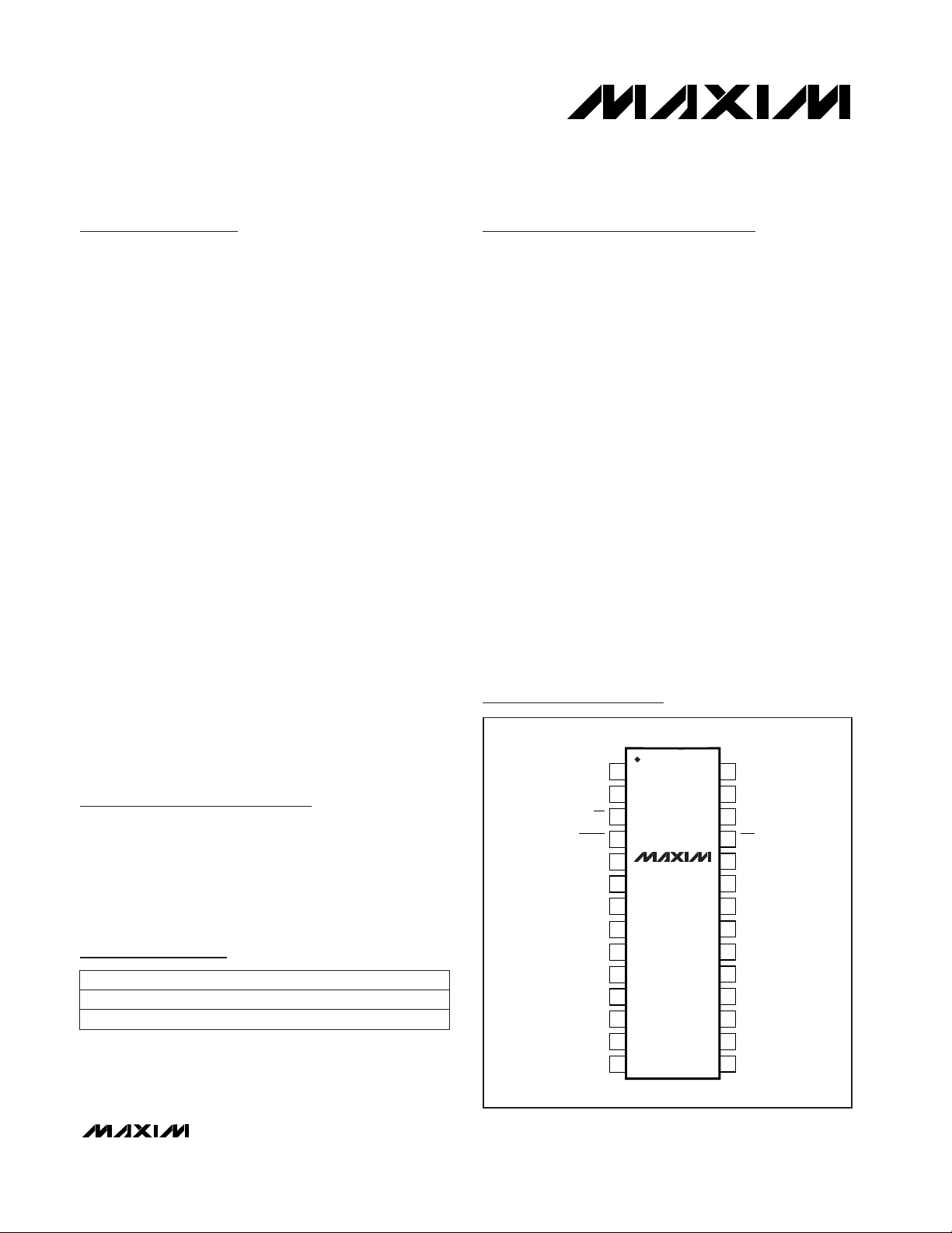
28
27
26
25
24
23
22
21
20
19
18
17
16
15
1
2
3
4
5
6
7
8
9
10
11
12
13
14
SCLK
DIN
DOUT
INT
V
DD
DGND
AIN5
CALOFF+
CALOFFREFIN+
REFINCALGAIN+
CALGAINAIN6
AIN4
AIN3
AIN2
AIN1
V+
AGND
ADCIN-
ADCIN+
MUXOUT-
MUXOUT+
RESET
CS
CLKOUT
CLKIN
SSOP
TOP VIEW
MAX1400
SPI and QSPI are trademarks of Motorola, Inc.
Pin Configuration
Ordering Information
PART
MAX1400CAI
MAX1400EAI -40°C to +85°C
0°C to +70°C
TEMP. RANGE PIN-PACKAGE
28 SSOP
28 SSOP
MAX1400
+5V, 18-Bit, Low-Power, Multichannel,
Oversampling (Sigma-Delta) ADC
2 _______________________________________________________________________________________
ABSOLUTE MAXIMUM RATINGS
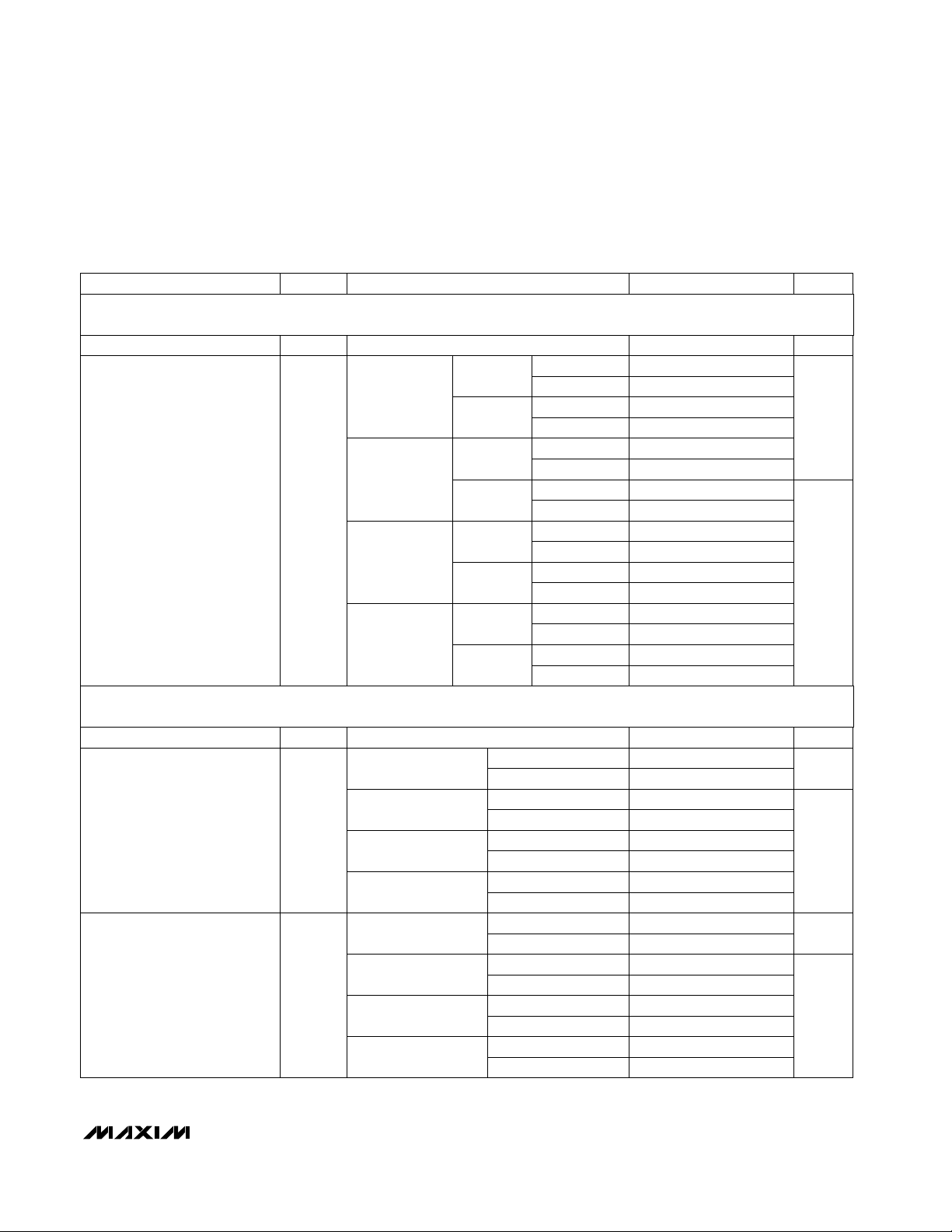
ELECTRICAL CHARACTERISTICS
(V+ = +5V ±5%, VDD= +2.7V to +5.25V, V
REFIN+
= +2.50V, REFIN- = AGND, f
CLKIN
= 2.4576MHz, TA= T
MIN
to T
MAX
, unless other-
wise noted. Typical values are at T
A
= +25°C.)
Stresses beyond those listed under “Absolute Maximum Ratings” may cause permanent damage to the device. These are stress ratings only, and functional
operation of the device at these or any other conditions beyond those indicated in the operational sections of the specifications is not implied. Exposure to
absolute maximum rating conditions for extended periods may affect device reliability.
V+ to AGND, DGND.................................................-0.3V to +6V
V
DD
to AGND, DGND...............................................-0.3V to +6V
AGND to DGND.....................................................-0.3V to +0.3V
Analog Inputs to AGND................................-0.3V to (V+ + 0.3V)
Analog Outputs to AGND.............................-0.3V to (V+ + 0.3V)
Reference Inputs to AGND...........................-0.3V to (V+ + 0.3V)
CLKIN and CLKOUT to DGND...................-0.3V to (V
DD
+ 0.3V)
All Other Digital Inputs to DGND..............................-0.3V to +6V
All Digital Outputs to DGND.......................-0.3V to (V
DD
+ 0.3V)
Maximum Current Input into Any Pin ..................................50mA
Continuous Power Dissipation (TA= +70°C)
28-Pin SSOP (derate 9.52mW/°C above +70°C) ........524mW
Operating Temperature Ranges
MAX1400CAI .....................................................0°C to +70°C
MAX1400EAI...................................................-40°C to +85°C
Storage Temperature Range.............................-60°C to +150°C
Lead Temperature (soldering, 10sec).............................+300°C
Bipolar Negative Full-Scale Drift
0.3
µV/°C
For gains of 8, 16, 32, 64, 128
PARAMETER SYMBOL MIN TYP MAX UNITS
Unipolar Offset Error -1 2 %FSR
Nominal Gain (Note 1) 0.98
Integral Nonlinearity INL -0.0015 0.0015 %FSR
Output Noise Table 16
0.5
Unipolar Offset Drift
0.3
µV/°C
Bipolar Zero Error -2.0 2.0 %FSR
0.8
Noise-Free Resolution 16 Bits
Bipolar Zero Drift
0.3
Positive Full-Scale Error
(Note 2)
-2.5 2.5
%FSR
Full-Scale Drift (Note 3)
0.8
0.3
µV/°C
-2 2
Gain Error (Note 4)
-3 3
%FSR
1
Gain-Error Drift (Note 5)
5
ppm/°C
-2.5 2.5
%FSR
0.8
CONDITIONS
For gains of 8, 16, 32, 64, 128
Relative to nominal offset of 1% FSR
For gains of 1, 2, 4, 8, 16, 32, 64
Bipolar mode, filter settings with FS1 = 0
Depends on filter setting and selected gain
For gains of 1, 2, 4
For gains of 8, 16, 32, 64, 128
For gains of 1, 2, 4
For gains of 1, 2, 4
For gains of 8, 16, 32, 64, 128
For gains of 1, 2, 4, 8, 16, 32, 64
For gain of 128
For gains of 1, 2, 4, 8, 16, 32, 64
For gain of 128
For gains of 1, 2, 4, 8, 16, 32, 64
No missing codes guaranteed by design;
for filter settings with FS1 = 0
For gains of 1, 2, 4
µV/°C
For gain of 128 -3.5 3.5
Bipolar Negative Full-Scale Error
-3.5 3.5For gain of 128
STATIC PERFORMANCE
MAX1400
+5V, 18-Bit, Low-Power, Multichannel,
Oversampling (Sigma-Delta) ADC
________________________________________________________________________________________ 3
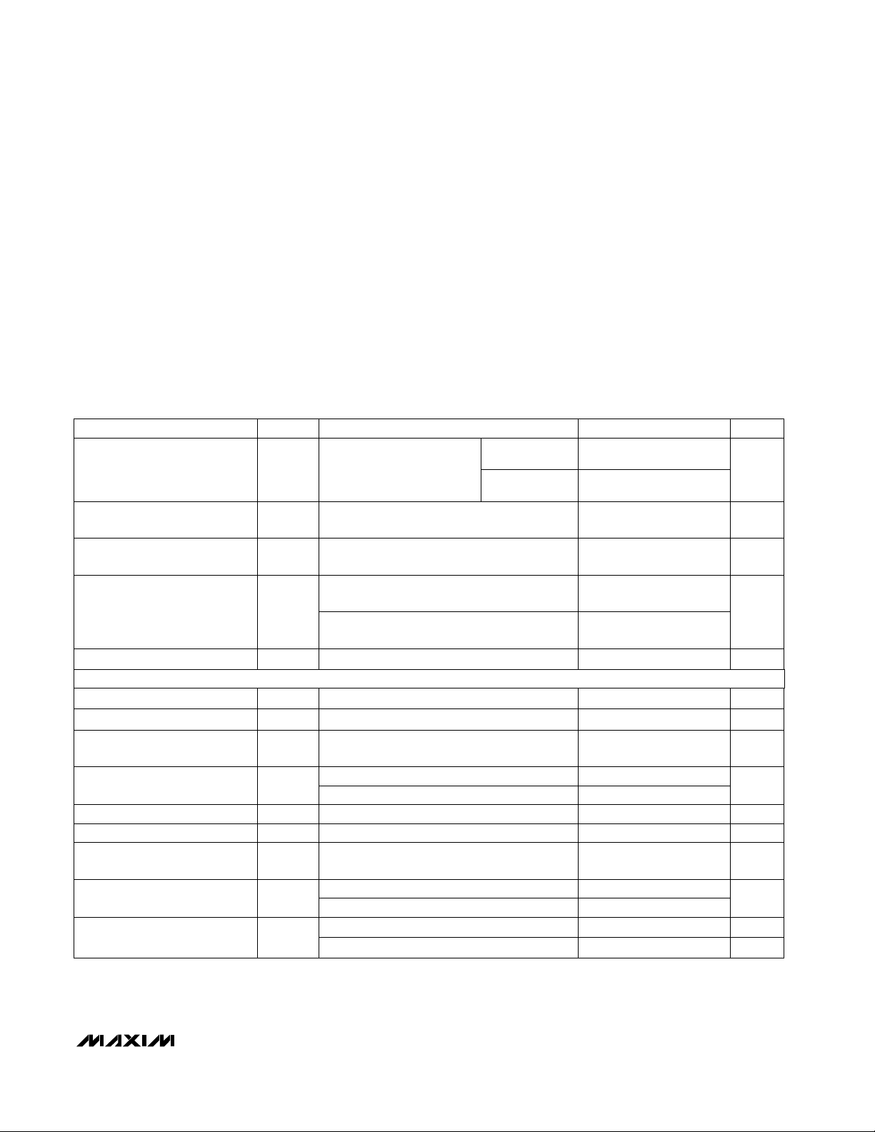
ELECTRICAL CHARACTERISTICS (continued)
(V+ = +5V ±5%, VDD= +2.7V to +5.25V, V
REFIN+
= +2.50V, REFIN- = AGND, f
CLKIN
= 2.4576MHz, TA= T
MIN
to T
MAX
, unless other-
wise noted. Typical values are at T
A
= +25°C.)
Unipolar mode
CONDITIONS
-116.7 116.7
Bipolar mode
UNITSMIN TYP MAXSYMBOLPARAMETER
%FSR
-58.35 58.35
Offset DAC Range (Note 6)
Input referred %FSR-2.5 2.5Offset DAC Full-Scale Error
For filter notch 50Hz, ±0.02 · f
NOTCH
,
MF1 = 0, MF0 = 0, f
CLKIN
= 2.4576MHz (Note 8)
DAC code = 0000
For filter notch 50Hz, ±0.02 · f
NOTCH
,
MF1 = 0, MF0 = 0, f
CLKIN
= 2.4576MHz
150
dB100NMR
Normal Mode 50Hz Rejection
(Note 8)
At DC
µV
RMS
0
Additional Noise from Offset
DAC (Note 7)
90
REFIN and AIN for BUFF = 0 VV
AGND
V+
Common-Mode Voltage Range
(Note 9)
BUFF = 1
BUFF = 1 10AIN Input Current (Note 10) nA
V
V
AGND
V+
+ 200mV - 1.5
Absolute and Common-Mode
AIN Voltage Range
pA40
DC Input Leakage Current
(Note 10)
Unipolar mode 16.7
Bipolar mode
%FSR
8.35
Offset DAC Resolution
For filter notch 60Hz, ±0.02 · f
NOTCH
,
MF1 = 0, MF0 = 0, f
CLKIN
= 2.4576MHz (Note 8)
dB
150
CMRCommon-Mode Rejection
For filter notch 60Hz, ±0.02 · f
NOTCH
,
MF1 = 0, MF0 = 0, f
CLKIN
= 2.4576MHz
dB100NMR
Normal Mode 60Hz Rejection
(Note 8)
REFIN and AIN for BUFF = 0 V
V
AGND
V+
- 30mV + 30mV
Absolute Voltage Range Input
REFIN and AIN for
BUFF = 0
TA= +25°C
TA= T
MIN
to T
MAX
10 nA
34
38
45
BUFF = 0
60
BUFF = 1, all gains 30
AIN Input Capacitance
(Note 11)
pF
Bipolar input range (U/B bit = 0)
±V
REF
/
gain
AIN Differential Voltage Range
(Note 12)
V
Gain = 1
Gain = 2
Gain = 4
Gain = 8, 16, 32, 64, 128
Unipolar input range (U/B bit = 1)
0 to V
REF
/
gain
%FSR0Offset DAC Zero-Scale Error
OFFSET DAC
ANALOG INPUTS/REFERENCE INPUTS (Specifications for AIN and REFIN, unless otherwise noted.)
Power-Supply Rejection V+ (Note 16) dBPSR
MAX1400
+5V, 18-Bit, Low-Power, Multichannel,
Oversampling (Sigma-Delta) ADC
4 _______________________________________________________________________________________
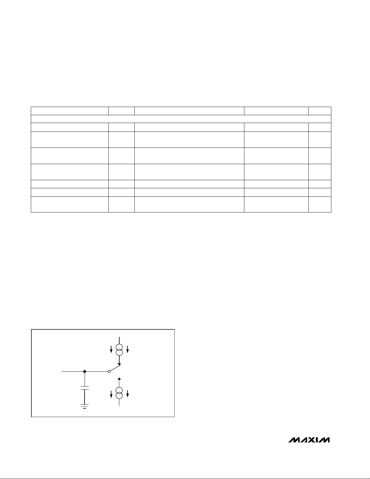
ELECTRICAL CHARACTERISTICS (continued)
(V+ = +5V ±5%, VDD= +2.7V to +5.25V, V
REFIN+
= +2.50V, REFIN- = AGND, f
CLKIN
= 2.4576MHz, TA= T
MIN
to T
MAX
, unless other-
wise noted. Typical values are at T
A
= +25°C.)
CONDITIONS UNITSMIN TYP MAXSYMBOLPARAMETER
0.8
0.8
All inputs except
CLKIN
0.4
µA-10 +10I
IN
Input Current
200
CLKIN only
All inputs except
CLKIN
mV
200
V
HYS
Input Hysteresis
DOUT
and INT
0.4
pF9C
O
Floating State Output
Capacitance
µA-10 10I
L
Floating State Leakage Current
V
0.4
V
IL
Input Low Voltage
±5% for specified performance; functional with
lower V
REF
V2.50
REFIN+ - REFIN- Voltage
(Note 13)
VDD= 5V
VDD= 3.3V
VDD= 5V
VDD= 3.3V
VDD= 5V
VDD= 3.3V
VDD= 5V
VDD= 3.3V
2
3.5
All inputs except
CLKIN
2
CLKIN only
V
2.4
V
IH
Input High Voltage
VDD= 5V
VDD= 3.3V
µA0.1I
BO
Current
%±10Initial Tolerance
%/°C±0.05Drift
Hz(Table 15)f
S
AIN and REFIN Input Sampling
Frequency
CLKOUT
V
0.4
V
OL
Output Low Voltage (Note 14)
VDD= 5V, I
SINK
= 800µA
VDD= 3.3V, I
SINK
= 100µA
VDD= 5V, I
SINK
= 10µA
VDD= 3.3V, I
SINK
= 10µA
CLKOUT
V
VDD- 0.3
V
OH
Output High Voltage (Note 14)
4
VDD= 5V, I
SOURCE
= 200µA
VDD= 3.3V, I
SOURCE
= 100µA
VDD= 5V, I
SOURCE
= 10µA
DOUT
and INT
VDD- 0.3
4
VDD= 3.3V, I
SOURCE
= 10µA
For specified performance V4.75 5.25V+V+ Voltage
V2.7 5.25V
DD
VDDVoltage
dB(Note 17)PSR
Power-Supply Rejection V+
(Note 16)
TRANSDUCER BURN-OUT (Note 15)
LOGIC OUTPUTS
LOGIC INPUTS
POWER REQUIREMENTS
MAX1400
+5V, 18-Bit, Low-Power, Multichannel,
Oversampling (Sigma-Delta) ADC
_______________________________________________________________________________________ 5
ELECTRICAL CHARACTERISTICS (continued)
(V+ = +5V ±5%, VDD= +2.7V to +5.25V, V
REFIN+
= +2.50V, REFIN- = AGND, f
CLKIN
= 2.4576MHz, TA= T
MIN
to T
MAX
, unless other-
wise noted. Typical values are at T
A
= +25°C.)
2.4576MHz
1.024MHz
Buffers off
Buffers off
Buffers on
2.4576MHz
1.024MHz
370 420
Buffers off
Buffers off
Buffers on
Normal mode,
MF1 = 0,
MF0 = 0
610 700
250 300
Buffers on 610
Buffers on
2X mode,
MF1 = 0,
MF0 = 1
1.2 1.5
CONDITIONS
PD bit = 1, external clock stopped
0.42 0.55
245
2.4576MHz
1.024MHz
Buffers off
Buffers off
Buffers on
2.4576MHz
1.024MHz
1.2
Buffers off
Buffers off
Buffers on
4X mode,
MF1 = 1,
MF0 = 0
µA
4.8 6
110
1.8 2.2
Buffers on 4.8
Buffers on
8X mode,
MF1 = 1,
MF0 = 1
mA
4.8 6
I
V+
V+ Current
1.8 2.2
1.8
0.42
V+ Standby Current (Note 18)
0.08
70 200
2X mode,
MF1 = 0, MF0 = 1
0.17 0.35
0.13
Normal mode,
MF1 = 0, MF0 = 0
PD bit = 1, external clock stopped 110
150 300
µAVDDStandby Current (Note 18)
µA
150 300
2X mode,
MF1 = 0, MF0 = 1
1.024MHz
2.4576MHz
0.28 0.50
Normal mode,
MF1 = 0, MF0 = 0
1.024MHz
175 210
2.4576MHz
0.15
0.11
8X mode,
MF1 = 1, MF0 = 1
0.32 0.45
mA
4X mode,
MF1 = 1, MF0 = 0
0.22 0.40
235 450
µA
1.024MHz
1.024MHz
2.4576MHz
I
DD
3.3V Digital Supply Current
1.024MHz
2.4576MHz
2.4576MHz
1.024MHz
2.4576MHz
0.24
0.17
8X mode,
MF1 = 1, MF0 = 1
0.53 0.80
mA
4X mode,
MF1 = 1, MF0 = 0
0.36 0.60
1.024MHz
2.4576MHz
I
DD
5V Digital Supply Current
1.024MHz
2.4576MHz
UNITSMIN TYP MAXSYMBOLPARAMETER
ANALOG POWER-SUPPLY CURRENT (Measured with digital inputs at either DGND or VDD, external CLKIN, burn-out currents
disabled, X2CLK = 0, CLK = 0 for 1.024MHz, CLK = 1 for 2.4576MHz.)
DIGITAL POWER-SUPPLY CURRENT (Measured with digital inputs at either DGND or VDD, external MCLKIN, burn-out currents
disabled, X2CLK = 0, CLK = 0 for 1.024MHz, CLK = 1 for 2.4576MHz.)
µA

MAX1400
+5V, 18-Bit, Low-Power, Multichannel,
Oversampling (Sigma-Delta) ADC
6 _______________________________________________________________________________________
Note 1: Nominal gain is 0.98. This ensures a full-scale input voltage may be applied to the part under all conditions without caus-
ing saturation of the digital output data.
Note 2: Positive Full-Scale Error includes zero-scale errors (unipolar offset error or bipolar zero error) and applies to both unipolar
and bipolar input ranges. This error does not include the nominal gain of 0.98.
Note 3: Full-Scale Drift includes zero-scale drift (unipolar offset drift or bipolar zero drift) and applies to both unipolar and bipolar
input ranges.
Note 4: Gain Error does not include zero-scale errors. It is calculated as (full-scale error - unipolar offset error) for unipolar ranges
and as (full-scale error - bipolar zero error) for bipolar ranges. This error does not include the nominal gain of 0.98.
Note 5: Gain-Error Drift does not include unipolar offset drift or bipolar zero drift. It is effectively the drift of the part if zero-scale
error is removed.
Note 6: Use of the offset DAC does not imply that any input may be taken below AGND.
Note 7: Additional noise added by the offset DAC is dependent on the filter cutoff, gain, and DAC setting. No noise is added for a
DAC code of 0000.
Note 8: Guaranteed by design or characterization; not production tested.
Note 9: The input voltage must be within the Absolute Input Voltage Range specification.
Note 10: All AIN and REFIN pins have identical input structures. Leakage is production tested only for the AIN3, AIN4, AIN5,
CALGAIN, and CALOFF inputs.
Note 11: The dynamic load presented by the MAX1400 analog inputs for each gain setting is discussed in detail in the
Switching
Network
section.Values are provided for the maximum allowable external series resistance. Note that this value does not
include any additional capacitance added by the user to the MUXOUT_ or ADCIN_ pins.
Note 12: The input voltage range for the analog inputs is with respect to the voltage on the negative input of its respective differen-
tial or pseudo-differential pair. Table 5 shows which inputs form differential pairs.
Note 13: V
REF
= V
REFIN+
- V
REFIN-
.
Note 14: These specifications apply to CLKOUT only when driving a single CMOS load.
Note 15: The burn-out currents require a 500mV overhead between the analog input voltage and both V+ and AGND to operate
correctly.
ELECTRICAL CHARACTERISTICS (continued)
(V+ = +5V ±5%, VDD= +2.7V to +5.25V, V
REFIN+
= +2.50V, REFIN- = AGND, f
CLKIN
= 2.4576MHz, TA= T
MIN
to T
MAX
, unless other-
wise noted. Typical values are at T
A
= +25°C.)
2.4576MHz
1.024MHz
Buffers off
Buffers off
Buffers on
2.4576MHz
1.024MHz
2.43 3.60
Buffers off
Buffers off
Buffers on
Normal mode,
MF1 = 0,
MF0 = 0
4.23 5.75
2.43 3.75
Buffers on 3.70
Buffers on
2X mode,
MF1 = 0,
MF0 = 1
7.4 10.0
CONDITIONS
3.50 5.25
1.88
2.4576MHz
1.024MHz
Buffers off
Buffers off
Buffers on
2.4576MHz
1.024MHz
6.85
Buffers off
Buffers off
Buffers on
4X mode,
MF1 = 1,
MF0 = 0
25.8 33.0
10.8 14.0
Buffers on 25.2
Buffers on
8X mode,
MF1 = 1,
MF0 = 1
mW
26.7 34.0
PDPower Dissipation
11.7 15.0
10.2
2.95
(Note 18) 10 100 µWStandby Power Dissipation
1.45 2.55
UNITSMIN TYP MAXSYMBOLPARAMETER
5V POWER DISSIPATION (V+ = VDD= +5V, digital inputs = 0 or VDD, external CLKIN, burn-out currents disabled, X2CLK = 0,
CLK = 0 for 1.024MHz, CLK = 1 for 2.4576MHz.)
MAX1400
+5V, 18-Bit, Low-Power, Multichannel,
Oversampling (Sigma-Delta) ADC
_______________________________________________________________________________________ 7
Note 16: Measured at DC in the selected passband. PSR at 50Hz will exceed 120dB with filter notches of 25Hz or 50Hz and FAST
bit = 0. PSR at 60Hz will exceed 120dB with filter notches of 20Hz or 60Hz and FAST bit = 0.
Note 17: PSR depends on gain. For a gain of +1V/V, PSR is 70dB typical. For a gain of +2V/V, PSR is 75dB typical. For a gain of
+4V/V, PSR is 80dB typical. For gains of +8V/V to +128V/V, PSR is 85dB typical.
Note 18: Standby power-dissipation and current specifications are valid only with CLKIN driven by an external clock and with the
external clock stopped. If the clock continues to run in standby mode, the power dissipation will be considerably higher.
When used with a resonator or crystal between CLKIN and CLKOUT, the actual power dissipation and I
DD
in standby
mode will depend on the resonator or crystal type.
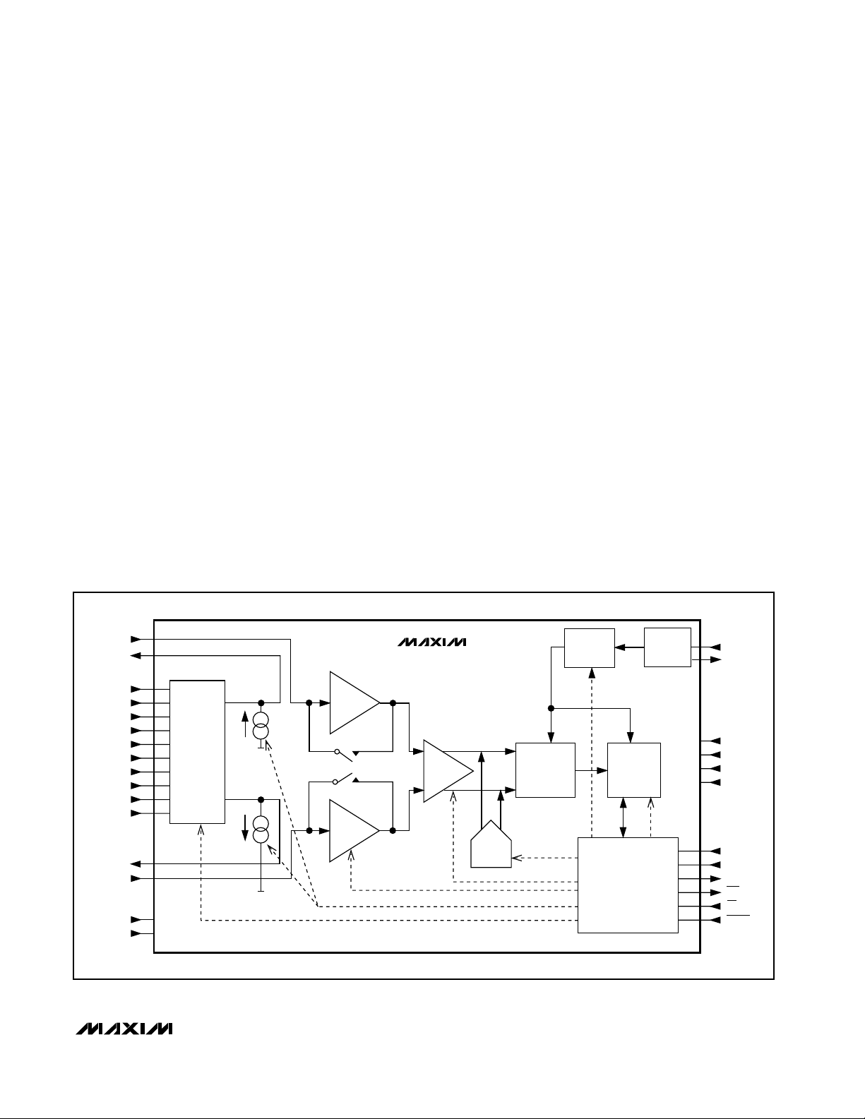
TIMING CHARACTERISTICS
(V+ = +5V ±5%, VDD= +2.7V to +5.25V, AGND = DGND, f
CLKIN
= 2.4576MHz; input logic 0 = 0V; logic 1 = VDD, TA= T
MIN
to T
MAX
,
unless otherwise noted.) (Notes 19, 20, 21)
0 100VDD= 3.3V
VDD= 5V
VDD= 3.3V
VDD= 5V
Bus Relinquish Time After SCLK
Rising Edge (Note 26)
t
10
10 100
ns
SCLK Falling Edge to Data Valid
Delay (Notes 24, 25)
t
6
080
ns
INT High Time
t
INT
560 / N
· t
CLKIN
ns
X2CLK = 1, N = 2
(2 · MF1 + MF0)
X2CLK = 1
X2CLK = 0
SCLK Setup to Falling Edge CS
t
4
30 ns
SCLK Low Pulse Width t
8
100 ns
10 70
100 nsVDD= 5V
CS Rising Edge to SCLK Rising
Edge Hold Time (Note 21)
t
9
0 ns
SCLK High Pulse Width t
7
100 ns
CS Falling Edge to SCLK Falling
Edge Setup Time
t
5
30 ns
280 / N
· t
CLKIN
INT to CS Setup Time (Note 8)
t
3
X2CLK = 0, N = 2
(2 · MF1 + MF0)
0 ns
RESET Pulse Width Low
t
2
100 ns
Master Clock Input Low Time f
CLKIN LO
0.4 ·
t
CLKIN
nst
CLKIN
= 1 / f
CLKIN
, X2CLK = 0
Master Clock Input High Time f
CLKIN HI
0.4 ·
t
CLKIN
nst
CLKIN
= 1 / f
CLKIN
, X2CLK = 0
Master Clock Frequency f
CLKIN
0.8 5.0
MHz
Crystal oscillator or clock
externally supplied for
specified performance
(Notes 22, 23)
PARAMETER SYMBOL MIN TYP MAX UNITS
0.4 2.5
CONDITIONS
SCLK Rising Edge to INT High
(Note 27)
t
11
200 nsVDD= 3.3V
SERIAL-INTERFACE READ OPERATION
MAX1400
+5V, 18-Bit, Low-Power, Multichannel,
Oversampling (Sigma-Delta) ADC
8 _______________________________________________________________________________________
TIMING CHARACTERISTICS (continued)
(V+ = +5V ±5%, VDD= +2.7V to +5.25V, AGND = DGND, f
CLKIN
= 2.4576MHz; input logic 0 = 0V; logic 1 = VDD, TA= T
MIN
to T
MAX
,
unless otherwise noted.) (Notes 19, 20, 21)
Note 19: All input signals are specified with t
r
= tf= 5ns (10% to 90% of VDD).
Note 20: See Figure 4.
Note 21: Timings shown in tables are for the case where SCLK idles high between accesses. The part may also be used with the
SCLK idling low between accesses, provided CS is toggled. In this case SCLK in the timing diagrams should be inverted
and the terms “SCLK Falling Edge” and “SCLK Rising Edge” exchanged in the specification tables. If CS is permanently
tied low, the part should only be operated with SCLK idling high between accesses.
Note 22: CLKIN duty cycle range is 45% to 55%. CLKIN must be supplied whenever the MAX1400 is not in standby mode. If no
clock is present, the device can draw higher current than specified.
Note 23: The MAX1400 is production tested with f
CLKIN
at 2.5MHz (1MHz for some IDDtests).
Note 24: Measured with the load circuit of Figure 1 and defined as the time required for the output to cross the V
OL
or VOHlimits.
Note 25: For read operations, SCLK active edge is falling edge of SCLK.
Note 26: Derived from the time taken by the data output to change 0.5V when loaded with the circuit of Figure 1. The number is then
extrapolated back to remove effects of charging or discharging the 50pF capacitor. This ensures that the times quoted in
the timing characteristics are true bus-relinquish times and are independent of external bus loading capacitances.
Note 27: INT returns high after the first read after an output update. The same data can be read again while INT is high, but be
careful not to allow subsequent reads to occur close to the next output update.
CS Rising Edge to SCLK Rising
Edge Hold Time
t
18
0 ns
SCLK High Pulse Width t
16
100 ns
SCLK Low Pulse Width t
17
100 ns
Data Valid to SCLK Rising Edge
Hold Time
t
15
0 ns
PARAMETER SYMBOL MIN TYP MAX UNITS
CS Falling Edge to SCLK Falling
Edge Setup Time
t
13
30 ns
Data Valid to SCLK Rising Edge
Setup Time
t
14
30 ns
SCLK Setup to Falling Edge CS
t
12
30 ns
CONDITIONS
SERIAL-INTERFACE WRITE OPERATION
800µA
at V
DD
= +5V
100µA
at VDD = +3.3V
100µA
at V
DD
= +3.3V
TO
OUTPUT
PIN
50pF
200µA
at V
DD
= +5V
Figure 1. Load Circuit for Bus Relinquish Time and VOLand
V
OH
Levels

MAX1400
+5V, 18-Bit, Low-Power, Multichannel,
Oversampling (Sigma-Delta) ADC
_______________________________________________________________________________________ 9
Pin Description
15 AIN5
Analog Input Channel 5. Used as a differential or pseudo-differential input with AIN6 (see
Communications Register
section).
NAME FUNCTION
1 CLKIN
Clock Input. A crystal can be connected across CLKIN and CLKOUT. Alternatively, drive CLKIN with a
CMOS-compatible clock at a nominal frequency of 2.4576MHz or 1.024MHz, and leave CLKOUT unconnected. Frequencies of 4.9152MHz and 2.048MHz may be used if the X2CLK control bit is set to 1.
PIN
2 CLKOUT
Clock Output. When deriving the master clock from a crystal, connect the crystal between CLKIN and
CLKOUT. In this mode, the on-chip clock signal is not available at CLKOUT. Leave CLKOUT unconnected
when CLKIN is driven with an external clock.
3
CS
Chip-Select Input. Active-low logic input used to enable the digital interface. With CS hard-wired low, the
MAX1400 operates in its 3-wire interface mode with SCLK, DIN and DOUT used to interface to the device.
CS is used either to select the device in systems with more than one device on the serial bus, or as a
frame-synchronization signal for the MAX1400 when a continuous SCLK is used.
4
RESET
Active Low Reset Input. Drive low to reset the control logic, interface logic, digital filter and analog modulator to power-on status. RESET must be high and CLKIN must be toggling in order to exit reset.
5 MUXOUT+
Positive Analog Mux Output. The positive differential output signal from the part’s internal input multiplexer. Use this signal in conjunction with MUXOUT- and a high-quality external amplifier for additional signal
processing before conversion. Return the processed output through ADCIN+ and ADCIN-. Connect
MUXOUT+ directly to ADCIN+ if external processing is not required.
6 MUXOUT-
Negative Analog Mux Output. The negative differential output signal from the part’s internal input multiplexer. Use this signal in conjunction with MUXOUT+ and a high-quality external amplifier for additional
signal processing before conversion. Return the processed output through ADCIN+ and ADCIN-.
Connect MUXOUT- directly to ADCIN- if external processing is not required.
7 ADCIN+
Positive Analog Input. A direct input to the positive buffer and the positive differential input terminal of the
ADC, bypassing the input mux. This signal forms a differential input pair with ADCIN-. Connect ADCIN+ to
MUXOUT+ when direct access is not required.
8 ADCIN-
Negative Analog Input. A direct input to the negative buffer and the negative differential input terminal of
the ADC - bypassing the input mux. This signal forms a differential input pair with ADCIN+. Connect
ADCIN- to MUXOUT- when direct access is not required.
9 AGND Analog Ground. Reference point for the analog circuitry. AGND connects to the IC substrate.
10 V+ Analog Positive Supply Voltage (+4.75V to +5.25V)
11 AIN1
Analog Input Channel 1. May be used as a pseudo-differential input with AIN6 as common, or as the positive input of the AIN1/AIN2 differential analog input pair (see
Communications Register
section).
12 AIN2
Analog Input Channel 2. May be used as a pseudo-differential input with AIN6 as common, or as the negative input of the AIN1/AIN2 differential analog input pair (see
Communications Register
section).
13 AIN3
Analog Input Channel 3. May be used as a pseudo-differential input with AIN6 as common, or as the positive input of the AIN3/AIN4 differential analog input pair (see
Communications Register
section).
14 AIN4
Analog Input Channel 4. May be used as a pseudo-differential input with AIN6 as common, or as the negative input of the AIN3/AIN4 differential analog input pair (see
Communications Register
section).
16 AIN6
Analog Input 6. May be used as a common point for AIN1 through AIN5 in pseudo-differential mode, or as
the negative input of the AIN5/AIN6 differential analog input pair (see
Communications Register
section).

MAX1400
+5V, 18-Bit, Low-Power, Multichannel,
Oversampling (Sigma-Delta) ADC
10 ______________________________________________________________________________________
Pin Description (continued)
NAME FUNCTIONPIN
17 CALGAIN-
Negative Gain Calibration Input. Used for system-gain calibration. It forms the negative input of a fully
differential input pair with CALGAIN+. Normally these inputs are connected to reference voltages in the
system. When system gain calibration is not required and the auto-sequence mode is used, the
CALGAIN+/CALGAIN- input pair provides an additional fully differential input channel.
18 CALGAIN+
Positive Gain Calibration Input. Used for system gain calibration. It forms the positive input of a fully differential input pair with CALGAIN-. Normally these inputs are connected to reference voltages in the system.
When system gain calibration is not required and the auto-sequence mode is used, the CALGAIN+/
CALGAIN- input pair provides an additional fully differential input channel.
19 REFIN-
Negative Differential Reference Input. Bias REFIN- between V+ and AGND, provided that REFIN+ is more
positive than REFIN-.
20 REFIN+
Positive Differential Reference Input. Bias REFIN+ between V+ and AGND, provided that REFIN+ is more
positive than REFIN-.
21 CALOFF-
Negative Offset Calibration Input. Used for system offset calibration. It forms the negative input of a fully
differential input pair with CALOFF+. Normally these inputs are connected to zero-reference voltages in
the system. When system offset calibration is not required and the auto-sequence mode is used, the
CALOFF+/CALOFF- input pair provides an additional fully differential input channel.
22 CALOFF+
Positive Offset Calibration Input. Used for system offset calibration. It forms the positive input of a fully
differential input pair with CALOFF-. Normally these inputs are connected to zero-reference voltages in the
system. When system offset calibration is not required and the auto-sequence mode is used, the
CALOFF+/CALOFF- input pair provides an additional fully differential input channel.
23 DGND Digital Ground. Reference point for digital circuitry.
24 V
DD
Digital Supply Voltage (+2.7V to +5.25V)
25
INT
Interrupt Output. A logic low indicates that a new output word is available from the data register. INT
returns high upon completion of a full output word read operation. INT also returns high for short periods
(determined by the filter and clock control bits) if no data read has taken place. A logic high indicates
internal activity, and a read operation should not be attempted under this condition. INT can also provide
a strobe to indicate valid data at DOUT (MDOUT = 1).
26 DOUT
Serial Data Output. DOUT outputs data from the internal shift register containing information from the
Communications Register, Global Setup Registers, Transfer Function Registers, or Data Register. DOUT
can also provide the digital bit stream directly from the Σ-∆ modulator (MDOUT = 1).
27 DIN
Serial Data Input. Data on DIN is written to the input shift register and later transferred to the
Communications Register, Global Setup Registers, Special Function Register or Transfer Function
Registers, depending on the register selection bits in the Communications Register.
28 SCLK
Serial Clock Input. Apply an external serial clock to transfer data to and from the MAX1400. This serial
clock can be continuous, with data transmitted in a train of pulses, or intermittent. If CS is used to frame
the data transfer, then SCLK may idle high or low between conversions and CS determines the desired
active clock edge (see
Selecting Clock Polarity
). If CS is tied permanently low, SCLK must idle high
between data transfers.
MAX1400
+5V, 18-Bit, Low-Power, Multichannel,
Oversampling (Sigma-Delta) ADC
______________________________________________________________________________________ 11
_______________Detailed Description
Circuit Description
The MAX1400 is a low-power, multichannel, serialoutput, sigma-delta ADC designed for applications with
a wide dynamic range, such as weigh scales and pressure transducers. The functional block diagram in
Figure 2 contains a switching network, a modulator, a
PGA, two buffers, an oscillator, an on-chip digital filter,
and a bidirectional serial communications port.
Three fully-differential input channels feed into the
switching network. Each channel may be independently programmed with a gain between +1V/V and
+128V/V. These three differential channels may also be
configured to operate as five pseudo-differential input
channels. Two additional, fully differential system-calibration channels allow system gain and offset error to
be measured. These system-calibration channels can
be used as additional differential signal channels when
dedicated gain and offset error correction channels are
not required.
Two chopper-stabilized buffers are available to isolate
the selected inputs from the capacitive loading of the
PGA and modulator. Three independent DACs provide
compensation for the DC component of the input signal
on each of the differential input channels.
The sigma-delta modulator converts the input signal into
a digital pulse train whose average duty cycle represents
the digitized signal information. The pulse train is then
processed by a digital decimation filter, resulting in a
conversion accuracy exceeding 16 bits. The digital filter’s
decimation factor is user-selectable, which allows the
conversion result’s resolution to be reduced to achieve a
higher output data rate. When used with 2.4576MHz or
1.024MHz master clocks, the decimation filter can be
programmed to produce zeros in its frequency response
at the line frequency and associated harmonics. This
ensures excellent line rejection without the need for further post-filtering. In addition, the modulator sampling
frequency can be optimized for either lowest power dissipation or highest output data rate.
The MAX1400 can be configured to sequentially scan
all signal inputs and to transmit the results through the
serial interface with minimum communications overhead. The output word contains a result identification
tag to indicate the source of each conversion result.
MAX1400
SWITCHING
NETWORK
AGND
V+
ADCIN+
MUXOUT+
CALOFF+
CALGAIN+
AIN1
AIN2
AIN3
AIN4
AIN5
AIN6
CALOFF-
CALGAIN-
MUXOUT-
ADCIN-
REFIN+
REFIN-
BUFFER
PGA
DAC
MODULATOR
BUFFER
DIVIDER
CLOCK
GEN
CLKIN
CLKOUT
V
DD
DGND
V+
AGND
SCLK
DIN
DOUT
INT
CS
RESET
DIGITAL
FILTER
INTERFACE
AND CONTROL
Figure 2. Functional Diagram
 Loading...