

Page 1
General Description
The MAX1358/MAX1359/MAX1360 smart data-acquisition
systems (DAS) are each based on a 16-bit, sigma-delta
analog-to-digital converter (ADC) and system-support
functionality for a microprocessor (µP)-based system.
These devices integrate an ADC, DACs, operational
amplifiers, internal 1.25V/2.048V/2.5V selectable reference, temperature sensors, analog switches, a 32kHz
oscillator, a real-time clock (RTC) with alarm, a high-frequency-locked loop (FLL) clock, four user-programmable I/Os, an interrupt generator, and 1.8V and 2.7V
voltage monitors in a single chip.
The MAX1358/MAX1359/MAX1360 have dual 10:1 differential input multiplexers (muxes) that accept signal
levels from 0 to AVDD. An on-chip 1x to 8x programmable-gain amplifier (PGA) measures low-level signals
and reduces external circuitry required.
The MAX1358/MAX1359/MAX1360 operate from a single +1.8V to +3.6V supply and consume only 1.4mA in
normal mode and only 6.1µA in sleep mode.
The MAX1358 has two DACs with one uncommitted op
amp; the MAX1359 has one DAC with two uncommitted op amps; and the MAX1360 has three uncommitted op amps.
The serial interface is compatible with either SPI™/QSPI™
or MICROWIRE™, and is used to power up, configure,
and check the status of all functional blocks.
The MAX1358/MAX1359/MAX1360 are available in a
space-saving 40-pin TQFN package and are specified
over the commercial (0°C to +70°C) and the extended
(-40°C to +85°C) temperature ranges.
Applications
Battery-Powered and Portable Devices
Electrochemical and Optical Sensors
Medical Instruments
Industrial Control
Data-Acquisition Systems
Features
♦ +1.8V to +3.6V Single-Supply Operation
♦ Multichannel 16-Bit Sigma-Delta ADC
10sps to 512sps Programmable Conversion Rate
Self and System Offset and Gain Calibration
PGA with Gains of 1, 2, 4, or 8
Unipolar and Bipolar Modes
10-Input Differential Multiplexer
♦ 10-Bit Force-Sense DACs
♦ Uncommitted Op Amps
♦ Dual SPDT Analog Switches
♦ 1.25V, 2.048V, or 2.5V Selectable Voltage
Reference
♦ Internal Charge Pump
♦ System Support
Real Time Clock and Alarm Register
Internal/External Temperature Sensor
Internal Oscillator with Clock Output
User-Programmable I/O and Interrupt Generator
VDDMonitors
♦ SPI/QSPI/MICROWIRE, 4-Wire Serial Interface
♦ Space-Saving (6mm x 6mm x 0.8mm) 40-Pin TQFN
Package
MAX1358/MAX1359/MAX1360
16-Bit Data-Acquisition Systems with ADC, DACs,
UPIOs, RTC, Voltage Monitors, and Temp Sensor
________________________________________________________________ Maxim Integrated Products 1
Ordering Information
19-3710; Rev 1; 8/05
For pricing, delivery, and ordering information, please contact Maxim/Dallas Direct! at
1-888-629-4642, or visit Maxim’s website at www.maxim-ic.com.
PART
TEMP RANGE
PINPACKAGE
PKG
CODE
MAX1358AETL*
T4066-4
MAX1358BETL
T4066-4
MAX1358ACTL*
T4066-4
MAX1358BCTL*
T4066-4
MAX1359AETL*
T4066-4
MAX1359BETL
T4066-4
MAX1359ACTL*
T4066-4
MAX1359BCTL
T4066-4
MAX1360AETL*
T4066-4
MAX1360BETL*
T4066-4
MAX1360ACTL*
T4066-4
MAX1360BCTL*
T4066-4
SPI/QSPI are trademarks of Motorola, Inc.
MICROWIRE is a trademark of National Semiconductor Corp.
*Future product—contact factory for availability.
**EP = Exposed pad.
Pin Configurations appear at end of data sheet.
PART DACs OP AMPs
SPDT/SPST
SWITCHES
EXTERNAL ADC
INPUTS
UPIOs
MAX1358 2 1 2/2 2 4
MAX1359 1 2 2/1 2 4
MAX1360 0 3 2/0 2 4
Selector Guide
-40°C to +85°C 40 TQFN-EP**
-40°C to +85°C 40 TQFN-EP**
0°C to +70°C 40 TQFN-EP**
0°C to +70°C 40 TQFN-EP**
-40°C to +85°C 40 TQFN-EP**
-40°C to +85°C 40 TQFN-EP**
0°C to +70°C 40 TQFN-EP**
0°C to +70°C 40 TQFN-EP**
-40°C to +85°C 40 TQFN-EP**
-40°C to +85°C 40 TQFN-EP**
0°C to +70°C 40 TQFN-EP**
0°C to +70°C 40 TQFN-EP**
Page 2
MAX1358/MAX1359/MAX1360
16-Bit Data-Acquisition Systems with ADC, DACs,
UPIOs, RTC, Voltage Monitors, and Temp Sensor
2 _______________________________________________________________________________________
ABSOLUTE MAXIMUM RATINGS
ELECTRICAL CHARACTERISTICS
(AV
DD
= DVDD= +1.8V to +3.6V, V
REF
= +1.25V, external reference, CLK32K = 32.768kHz (external clock), C
REG
= 10µF, C
CPOUT
=
10µF, 10µF between CF+ and CF-, T
A
= T
MIN
to T
MAX
, unless otherwise noted. Typical values are at TA= +25°C.) (Note 1)
Stresses beyond those listed under “Absolute Maximum Ratings” may cause permanent damage to the device. These are stress ratings only, and functional
operation of the device at these or any other conditions beyond those indicated in the operational sections of the specifications is not implied. Exposure to
absolute maximum rating conditions for extended periods may affect device reliability.
AVDDto AGND .........................................................-0.3V to +4V
DV
DD
to DGND.........................................................-0.3V to +4V
AV
DD
to DV
DD
............................................................-4V to +4V
AGND to DGND.....................................................-0.3V to +0.3V
CLK32K to DGND....................................-0.3V to (DV
DD
+ 0.3V)
UPIO_ to DGND........................................................-0.3V to +4V
Digital Inputs to DGND ............................................-0.3V to +4V
Analog Inputs to AGND ...........................-0.3V to (AV
DD
+ 0.3V)
Digital Output to DGND…........................-0.3V to (DV
DD
+ 0.3V)
Analog Outputs to AGND.........................-0.3V to (AV
DD
+ 0.3V)
Continuous Current Into Any Pin.........................................50mA
Continuous Power Dissipation (T
A
= +70°C)
40-Pin TQFN (derate 25.6mW/°C above +70°C) ....2051.3mW
Operating Temperature Range
MAX13_ _ CTL ....................................................0°C to +70°C
MAX13_ _ ETL .................................................-40°C to +85°C
Junction Temperature......................................................+150°C
Storage Temperature Range .............................-65°C to +150°C
Lead Temperature (soldering, 10s) .................................+300°C
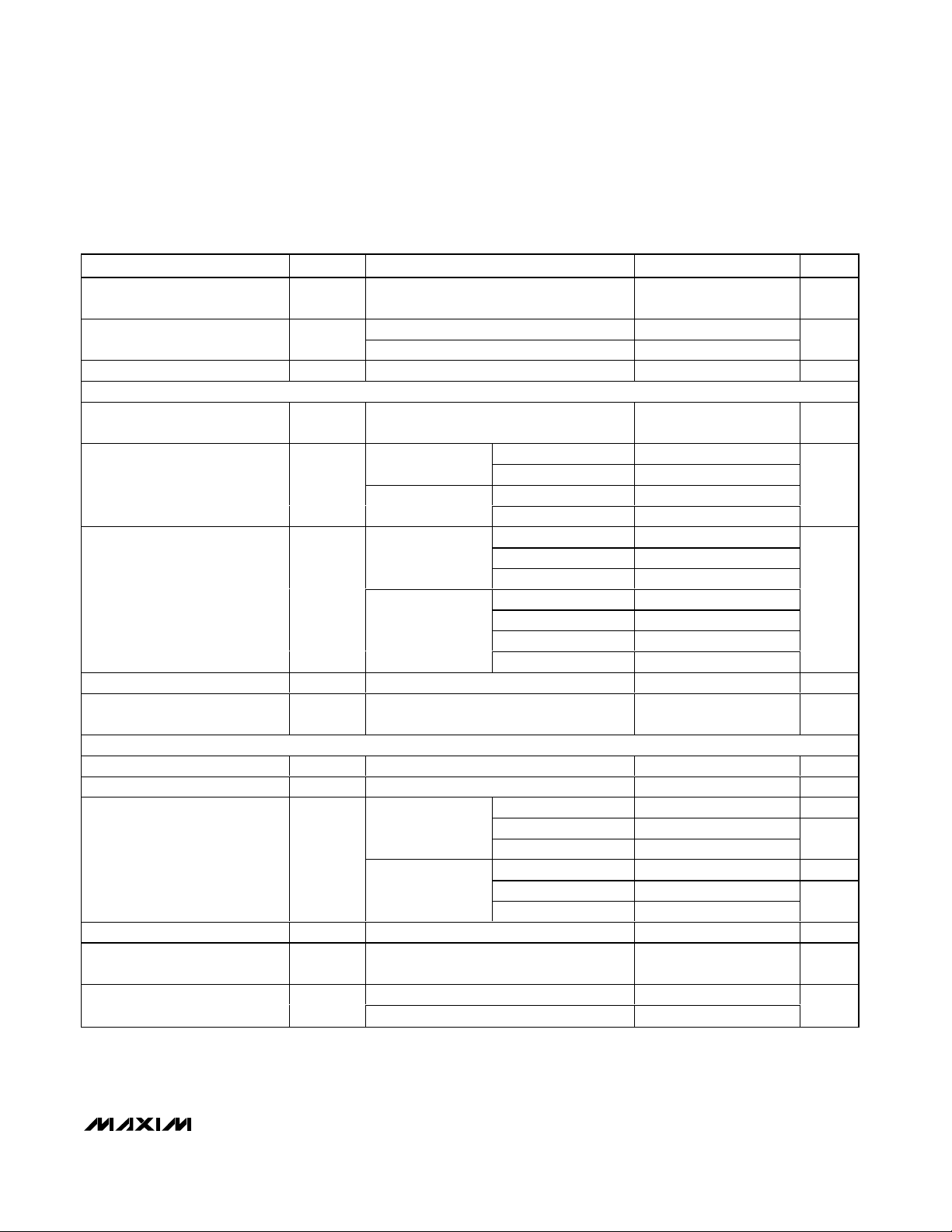
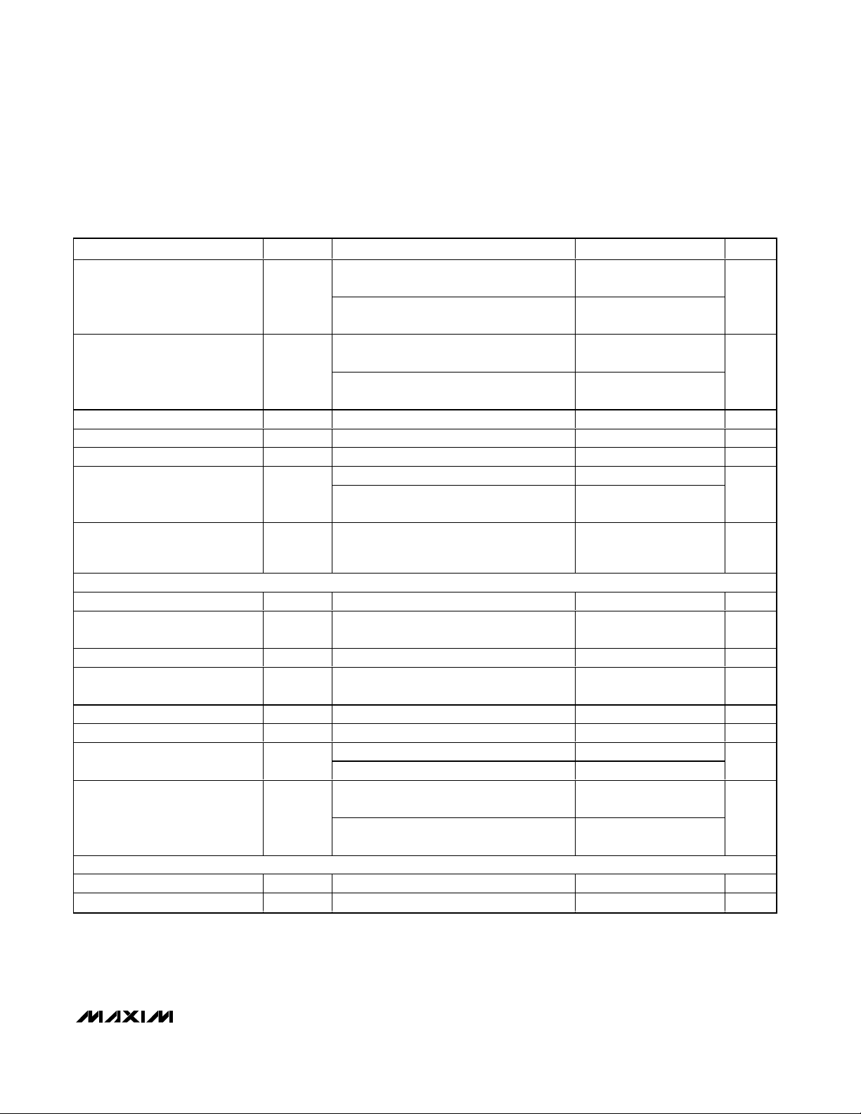
PARAMETER
CONDITIONS
UNITS
ADC DC ACCURACY
Noise-Free Resolution
Data rate = 10sps, PGA gain = 2;
data rate = 10sps to 60sps, PGA gain = 1;
no missing codes, Table 1 (Note 2)
16 Bits
Conversion Rate No missing codes, Table 1 10 512 sps
Output Noise No missing codes
µV
RMS
Integral Nonlinearity INL
Unipolar mode, AV
DD
= 3V, data
rate = 40sps, PGA gain = 1,
T
A
= +25°C
%FSR
Uncalibrated
Unipolar Offset Error or Bipolar
Zero Error (Note 3)
%FSR
Bipolar
Unipolar Offset-Error or Bipolar
Zero-Error Temperature Drift
(Note 4)
Unipolar
µV/°C
Uncalibrated
Gain Error (Notes 3, 5)
Data rate = 10sps, PGA = 1, calibrated
% FSR
Gain-Error Temperature
Coefficient
(Notes 4, 6)
ppm/ °C
DC Positive Power-Supply
Rejection Ratio
PSRR
PGA gain = 1, unipolar mode, measured by
full-scale error with AV
DD
= 1.8V to 3.6V
73 dB
ADC ANALOG INPUTS (AIN1, AIN2)
DC Input Common-Mode
Rejection Ratio
CMRR PGA gain = 1, unipolar mode 85 dB
SYMBOL
MIN TYP MAX
Table 1
Data rate = 10sps, PGA gain = 1, calibrated ±0.003
A grade ±0.003
B grade ±0.004
±1.0
±2.0
±10
±0.6
±0.003
±1.0
Page 3
MAX1358/MAX1359/MAX1360
16-Bit Data-Acquisition Systems with ADC, DACs,
UPIOs, RTC, Voltage Monitors, and Temp Sensor
_______________________________________________________________________________________ 3
ELECTRICAL CHARACTERISTICS (continued)
(AV
DD
= DVDD= +1.8V to +3.6V, V
REF
= +1.25V, external reference, CLK32K = 32.768kHz (external clock), C
REG
= 10µF, C
CPOUT
=
10µF, 10µF between CF+ and CF-, T
A
= T
MIN
to T
MAX
, unless otherwise noted. Typical values are at TA= +25°C.) (Note 1)
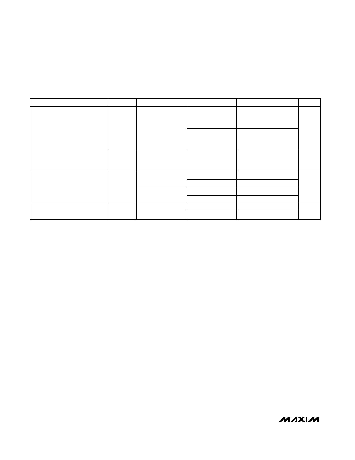
PARAMETER
CONDITIONS
UNITS
Normal-Mode 60Hz Rejection
Ratio
Data rate = 10sps or 60sps, PGA gain = 1,
unipolar mode (Note 2)
dB
Normal-Mode 50Hz Rejection
Ratio
Data rate = 10sps or 50sps, PGA gain = 1,
unipolar mode (Note 2)
dB
Absolute Input Range
V
Unipolar mode
-0.05 /
V
REF
/
Differential Input Range
Bipolar mode
-V
REF
/
V
REF
/
V
ADC not in measurement mode, mux
enabled, T
A
≤ +55°C, inputs = +0.1V to
(AV
DD
- 0.1V)
±1
DC Input Current (Note 7)
T
A
= +85°C ±5
nA
Input Sampling Capacitance C
IN
5pF
Input Sampling Rate
kHz
External Source Impedance at
Input
See Table 3
kΩ
FORCE-SENSE DAC (MAX1358/MAX1359 only, RL = 10kΩ and CL = 200pF, FBA = OUTA and FBB = OUTB, unless otherwise
noted)
Resolution Guaranteed monotonic 10 Bits
Differential Nonlinearity DNL Code 3D hex to 3FF hex ±1 LSB
A grade ±2
Integral Nonlinearity INL
Code 3D hex to 3FF
hex
B grade ±4
LSB
Offset Error Reference to code 52 hex ±20 mV
Offset-Error Tempco
µV/°C
Gain Error
±5 LSB
Gain-Error Tempco Excludes offset and reference drift ±1
ppm/°C
Input Leakage Current at SWA/B
SWA/B switches open (Notes 7, 8) ±1nA
±1nA
Input Leakage Current at FBA/B
V
FBA/B
= +0.3V to
(AV
DD
- 0.3V)
(Note 7)
pA
DAC Output Buffer Leakage
Current
DAC buffer disabled (Note 7) ±75 nA
Input Common-Mode Voltage At FBA and FBB 0
AV
DD
V
Line Regulation AVDD = +1.8V to +3.6V 40 175
µV/V
Load Regulation I
OUT
= ±2mA, CL = 1000pF (Note 2) 0.5
µV/µA
Output Voltage Range
V
SYMBOL
f
SAMPLE
Excludes offset and voltage reference error
TA = -40°C to +85°C
TA = 0°C to +70°C ±600
TA = 0°C to +50°C ±400
MIN TYP MAX
100
100
AGND AV
Gain
Gain
AGND AV
21.84
Table 3
±4.4
DD
Gain
Gain
0.35
DD
Page 4
MAX1358/MAX1359/MAX1360
16-Bit Data-Acquisition Systems with ADC, DACs,
UPIOs, RTC, Voltage Monitors, and Temp Sensor
4 _______________________________________________________________________________________
ELECTRICAL CHARACTERISTICS (continued)
(AV
DD
= DVDD= +1.8V to +3.6V, V
REF
= +1.25V, external reference, CLK32K = 32.768kHz (external clock), C
REG
= 10µF, C
CPOUT
=
10µF, 10µF between CF+ and CF-, T
A
= T
MIN
to T
MAX
, unless otherwise noted. Typical values are at TA= +25°C.) (Note 1)
PARAMETER
CONDITIONS
UNITS
Output Slew Rate
52 hex to 3FF hex code swing rising or
falling, R
L
= 10kΩ, CL = 100pF
40
V/ms
Output-Voltage Settling Time 10% to 90% rising or falling to ±0.5 LSB 65 µs
f = 0.1Hz to
10Hz
80
Input Voltage Noise
Referred to FBA/B,
f = 10Hz to
10kHz
µV
P-P
OUTA/B shorted to AGND 20
Output Short-Circuit Current
OUTA/B shorted to AV
DD
15
mA
Input-Output SWA/SWB Switch
Resistance
Between SWA and OUTA, or SWB and
OUTB, HFCK enabled
150 Ω
SWA/SWB Switch Turn-On/Off
Time
HFCK enabled
ns
Power-On Time Excluding reference 18 µs
EXTERNAL REFERENCE (REF)
Input Voltage Range
V
Input Resistance DAC on, internal REF and ADC off 2.5 MΩ
DC Input Leakage Current Internal REF, DAC, and ADC off (Note 7) 100 nA
INTERNAL VOLTAGE REFERENCE (C
REF
= 4.7µF)
A grade
AVDD ≥ +1.8V, TA = +25°C
B grade
A grade
AVDD ≥ +2.2V, TA = +25°C
B grade
A grade
2.5
Reference Output Voltage V
REF
AVDD ≥ +2.7V, TA = +25°C
B grade
2.5
V
15 50
A grade
V
REF
=
65
Output-Voltage Temperature
Coefficient (Note 7)
TC
B grade 15
ppm/oC
REF shorted to AGND 18 mA
Output Short-Circuit Current I
RSC
REF shorted to AV
DD
90 µA
A grade 100
Line Regulation TA = +25°C
B grade 25
µV/V
I
SOURCE
= 0
to 500µA
1.2
Load Regulation TA = +25°C, V
REF
= 1.25V
I
SINK
= 0 to
50µA
1.7
µV/µA
SYMBOL
MIN TYP MAX
excludes reference noise
V
= 1.25V
REF
2.048V, 2.5V
AGND AV
1.237 1.25 1.263
1.213 1.25 1.288
2.027 2.048 2.068
1.987 2.048 2.109
2.475
2.425
200
100
DD
2.525
2.575
Page 5
MAX1358/MAX1359/MAX1360
16-Bit Data-Acquisition Systems with ADC, DACs,
UPIOs, RTC, Voltage Monitors, and Temp Sensor
_______________________________________________________________________________________ 5
ELECTRICAL CHARACTERISTICS (continued)
(AV
DD
= DVDD= +1.8V to +3.6V, V
REF
= +1.25V, external reference, CLK32K = 32.768kHz (external clock), C
REG
= 10µF, C
CPOUT
=
10µF, 10µF between CF+ and CF-, T
A
= T
MIN
to T
MAX
, unless otherwise noted. Typical values are at TA= +25°C.) (Note 1)
PARAMETER
CONDITIONS
UNITS
Long-Term Stability (Note 9) 35
ppm/
1000hrs
f = 0.1Hz to 10Hz, AVDD = 3V 50
Output Noise Voltage
f = 10Hz to 10kHz, AV
DD
= 3V
µV
P-P
Turn-On Settling Time Buffer only, settle to 0.1% of final value
µs
TEMPERATURE SENSOR
Temperature Measurement
Resolution
ADC resolution is 16-bit, 10sps
°C/LSB
TA = 0°C to +70°C
A grade
T
A
= -40oC to +85°C ±1
TA = 0°C to +70°C
Internal Temperature-Sensor
Measurement Error
B grade
T
A
= -40°C to +85°C ±1
°C
TA = +25°C
TA = 0°C to +70°C ±1A grade
T
A
= -40°C to +85°C ±2
TA = 0°C to +70°C
External Temperature-Sensor
Measurement Error (Note 10)
B grade
T
A
= -40°C to +85°C ±1
°C
Temperature Measurement Noise
°C
RMS
Temperature Measurement
Power-Supply Rejection Ratio
0.2
°C/V
OP AMP (RL = 10kΩ connected to AV
DD
/ 2)
Input Offset Voltage V
OS
V
CM
= 0.5V ±15 mV
Offset-Error Tempco 3
µV/oC
TA = -40°C to +85°C
±1nA
TA = 0°C to +70°C4
IN1+, IN2+, IN3+
T
A
= 0°C to +50°C2
pA
TA = -40°C to +85°C
±1nA
TA = 0°C to +70°C20
Input Bias Current (Note 7) I
BIAS
IN1-, IN2-, IN3-
T
A
= 0°C to +50°C
pA
Input Offset Current I
OS
±1nA
Input Common-Mode Voltage
Range
CMVR 0
AVDD -
V
0 ≤ VCM ≤ 75mV 60
Common-Mode Rejection Ratio CMRR
75mV < V
CM
≤ AVDD - 0.35V 60 75
dB
SYMBOL
TA = +32°C to +43°C ±0.50
TA = +10°C to +50°C ±0.5
V
I N 1 _, I N 2 _
= + 0.3V to ( AV
- 0.3V ) ( N ote 7)
D D
MIN TYP MAX
400
100
0.11
±0.5
±0.5
±0.50
±0.5
0.18
0.006
±300
±200
0.025
±600
±400
0.35
Page 6
MAX1358/MAX1359/MAX1360
16-Bit Data-Acquisition Systems with ADC, DACs,
UPIOs, RTC, Voltage Monitors, and Temp Sensor
6 _______________________________________________________________________________________
ELECTRICAL CHARACTERISTICS (continued)
(AV
DD
= DVDD= +1.8V to +3.6V, V
REF
= +1.25V, external reference, CLK32K = 32.768kHz (external clock), C
REG
= 10µF, C
CPOUT
=
10µF, 10µF between CF+ and CF-, T
A
= T
MIN
to T
MAX
, unless otherwise noted. Typical values are at TA= +25°C.) (Note 1)
PARAMETER
CONDITIONS
UNITS
Power-Supply Rejection Ratio PSRR AVDD = +1.8V to +3.6V
dB
Large-Signal Voltage Gain A
VOL
90
dB
I
SOURCE
= 10µA
I
SOURCE
= 50µA
I
SOURCE
= 100µA
I
SOURCE
= 500µA
Sourcing
I
SOURCE
= 2m A 0.5
I
SINK
= 10µA
I
SINK
= 50µA
I
SINK
= 100µA
I
SINK
= 500µA
Maximum Current Drive ∆V
OUT
Sinking
I
SINK
= 2m A 0.5
V
Gain Bandwidth Product GBW Unity-gain configuration, CL = 1nF 80 kHz
Phase Margin
60
Degrees
Output Slew Rate SR CL = 200pF
V/µs
f = 0.1Hz to 10Hz 80
Input Voltage Noise
Unity-gain
configuration
f = 10Hz to 10kHz
µV
P-P
V
OUT_
shorted to AGND 20
Output Short-Circuit Current
V
OUT_
shorted to AV
DD
15
mA
Power-On Time 15 µs
SPDT SWITCHES (SNO_, SNC_, SCM_, HFCK enabled)
V
SCM_
= 0V
45
V
SCM_
= 0.5V
50
On-Resistance R
ON
150
Ω
±1nA
SNO_, SNC_ Off-Leakage
Current (Note 7)
)
)
SNO_, SNC_ = +0.5V,
+1.5V; SCM_ = +1.5V,
+0.5V
pA
±2
SCM_ Off-Leakage Current
(Note 7)
)
SNO_, SNC_ = +0.5V,
+1.5V; SCM_ = +1.5V,
+0.5V
nA
±2
SCM_ On-Leakage Current
(Note 7)
)
SNO_, SNC_ = +0.5V,
+1.5V, or floating;
nA
Input Voltage Range
V
Turn-On/Off Time
Break-before-make
ns
SYMBOL
100mV ≤ V
≤ AVDD - 100mV (Note 11)
OUT_
Unity-gain configuration, CL = 1nF (Note 11)
V
= 0.5V to AV
SCM_
TA = 0°C to +50°C
TA = 0°C to +50°C
DD
TA = -40°C to +85°C
I
SNO_(OFF
I
SNC_(OFF
I
SCM_(OFF
TA = 0°C to +70°C ±600
TA = 0°C to +50°C ±400
TA = -40°C to +85°C
TA = 0°C to +70°C ±1.2
TA = 0°C to +50°C ±0.8
TA = -40°C to +85°C
I
SCM_(ON
tON/t
SCM_ = +1.5V, +0.5V
OFF
TA = 0°C to +70°C ±1.2
T
= 0°C to +50°C ±0.8
A
MIN TYP MAX
76.5 100
116
0.04
200
AGND AV
100
0.005
0.025
0.05
0.25
0.005
0.025
0.05
0.25
DD
Page 7
MAX1358/MAX1359/MAX1360
16-Bit Data-Acquisition Systems with ADC, DACs,
UPIOs, RTC, Voltage Monitors, and Temp Sensor
_______________________________________________________________________________________ 7
ELECTRICAL CHARACTERISTICS (continued)
(AV
DD
= DVDD= +1.8V to +3.6V, V
REF
= +1.25V, external reference, CLK32K = 32.768kHz (external clock), C
REG
= 10µF, C
CPOUT
=
10µF, 10µF between CF+ and CF-, T
A
= T
MIN
to T
MAX
, unless otherwise noted. Typical values are at TA= +25°C.) (Note 1)
PARAMETER
CONDITIONS
UNITS
Input Capacitance
SNO_, SNC_, or SCM_ = AV
DD
or AGND;
switch connected to enabled mux input
5pF
CHARGE PUMP (10µF at REG and 10µF external capacitor between CF+ and CF-)
Maximum Output Current I
OUT
10 mA
No load 3.2 3.3 3.6
Output Voltage
I
OUT
= 10mA 3.0
V
Output Voltage Ripple
10µF external capacitor between CPOUT
and DGND, I
OUT
= 10mA, excluding ESR of
external capacitor
50 mV
Load Regulation
I
OUT
= 10mA, excluding ESR of external
capacitor
15 20
mV/mA
REG Input Voltage Range Internal linear regulator disabled 1.6 1.8 V
REG Input Current Linear regulator off, charge pump off 3 nA
CPOUT Input Voltage Range Charge pump disabled 1.8 3.6 V
CPOUT Input Leakage Current Charge pump disabled 2 nA
SIGNAL-DETECT COMPARATOR
TSEL[2:0] = 0 hex 0
TSEL[2:0] = 4 hex 50
TSEL[2:0] = 5 hex
TSEL[2:0] = 6 hex
Differential Input-Detection
Threshold Voltage
TSEL[2:0] = 7 hex
mV
Differential Input-Detection
Threshold Error
mV
Common-Mode Input Voltage
Range
V
Turn-On Time 50 µs
VOLTAGE MONITORS
DV
DD
Monitor Supply Voltage
Range
For valid reset 1.0 3.6 V
A grade
Trip Threshold (DVDD Falling)
B grade
V
DVDD Monitor Timeout Reset
Period
1.5 s
HYSE bit set to logic 1
DVDD Monitor Hysteresis
HYSE bit set to logic 0 35
mV
SYMBOL
MIN TYP MAX
AGND AV
1.80 1.85 1.90
1.80 1.85 1.95
100
150
200
±10
200
DD
Page 8
MAX1358/MAX1359/MAX1360
16-Bit Data-Acquisition Systems with ADC, DACs,
UPIOs, RTC, Voltage Monitors, and Temp Sensor
8 _______________________________________________________________________________________
ELECTRICAL CHARACTERISTICS (continued)
(AV
DD
= DVDD= +1.8V to +3.6V, V
REF
= +1.25V, external reference, CLK32K = 32.768kHz (external clock), C
REG
= 10µF, C
CPOUT
=
10µF, 10µF between CF+ and CF-, T
A
= T
MIN
to T
MAX
, unless otherwise noted. Typical values are at TA= +25°C.) (Note 1)
PARAMETER
CONDITIONS
UNITS
DVDD Monitor Turn-On Time 5ms
CPOUT Monitor Supply Voltage
Range
1.0 3.6 V
CPOUT Monitor Trip Threshold 2.7 2.8 2.9 V
CPOUT Monitor Hysteresis 35 mV
CPOUT Monitor Turn-On Time 5ms
Internal Power-On Reset Voltage
1.7 V
32kHz Oscillator (32KIN, 32KOUT)
Clock Frequency DVDD = 2.7V
kHz
Stability DVDD = 1.8V to 3.6V, excluding crystal 25
ppm
Oscillator Startup Time
ms
Crystal Load Capacitance 6pF
LOW-FREQUENCY CLOCK INPUT/OUTPUT (CLK32K)
Output Clock Frequency
kHz
Absolute Input to Output Clock
Jitter
Cycle to cycle 5 ns
Input to Output Rise/Fall Time 10% to 90%, 30pF load 5 ns
Input/Output Duty Cycle 40 60 %
HIGH-FREQUENCY CLOCK OUTPUT (CLK)
f
OUT
= f
FLL
f
OUT
= f
FLL
/ 2, power-up default
f
OUT
= f
FLL
/ 4
MHz
FLL Output Clock Frequency
f
OUT
= f
FLL
/ 8
kHz
Cycle to cycle, FLL off
Absolute Clock Jitter
Cycle to cycle, FLL on 1
ns
Rise and Fall Time tR/t
F
10% to 90%, 30pF load 10 ns
f
OUT
= 4.9152MHz 40 60
Duty Cycle
f
OUT
= 2.4576MHz, 1.2288MHz, 614.4kHz 45 55
%
Uncalibrated CLK Frequency
Error
FLL calibration not performed ±35 %
DIGITAL INPUTS (SCLK, DIN, CS, UPIO_, CLK32K)
Input High Voltage V
IH
0.7 x
V
Input Low Voltage V
IL
0.3 x
V
SYMBOL
MIN TYP MAX
32.768
1500
32.768
4.8660 4.9152 4.9644
2.4330 2.4576 2.4822
1.2165 1.2288 1.2411
608.25 614.4 620.54
0.15
DV
DD
DV
DD
Page 9
MAX1358/MAX1359/MAX1360
16-Bit Data-Acquisition Systems with ADC, DACs,
UPIOs, RTC, Voltage Monitors, and Temp Sensor
_______________________________________________________________________________________ 9
ELECTRICAL CHARACTERISTICS (continued)
(AV
DD
= DVDD= +1.8V to +3.6V, V
REF
= +1.25V, external reference, CLK32K = 32.768kHz (external clock), C
REG
= 10µF, C
CPOUT
=
10µF, 10µF between CF+ and CF-, T
A
= T
MIN
to T
MAX
, unless otherwise noted. Typical values are at TA= +25°C.) (Note 1)
PARAMETER
CONDITIONS
UNITS
DVDD supply voltage
0.7 x
UPIO_ Input High Voltage
CPOUT supply voltage
0.7 x
V
DVDD supply voltage
0.3 x
UPIO_ Input Low Voltage
CPOUT supply voltage
0.3 x
V
Input Hysteresis V
HYS
DVDD = 3.0V
mV
Input Current I
IN
VIN = DGND or DVDD (Note 7)
nA
Input Capacitance VIN = DGND or DV
DD
10 pF
VIN = DVDD or CPOUT, pullup enabled
1
UPIO_ Input Current
V
IN
= DVDD or CPOUT or 0V,
pullup disabled
1
µA
UPIO_ Pullup Current
V
IN
= 0V, pullup enabled, floating UPIO
inputs are pulled up to DV
DD
or CPOUT
with pullup enabled
0.5 2 5 µA
DIGITAL OUTPUTS (DOUT, RESET, UPIO_, CLK32K, INT, CLK)
Output Low Voltage V
OL
I
SINK
= 1mA 0.4 V
Output High Voltage V
OH
I
SOURCE
= 500µA
0.8 x
V
I
L
±1µA
DOUT Tri-State Output
Capacitance
C
OUT
15 pF
RESET Output Low Voltage V
OL
I
SINK
= 1mA 0.4 V
RESET Output Leakage Current Open-drain output, RESET deasserted 0.1 µA
I
SINK
= 1mA, UPIO_ referenced to DV
DD
0.4
UPIO_ Output Low Voltage V
OL
I
SINK
= 4mA, UPIO_ referenced to CPOUT 0.4
V
I
SOURCE
= 500µA, UPIO_ referenced to
DV
DD
0.8 x
UPIO_ Output High Voltage V
OH
I
SOURCE
= 4mA, UPIO_ referenced to
CPOUT
V
C P OU T
V
POWER REQUIREMENT
Analog Supply Voltage Range AV
DD
1.8 3.6 V
Digital Supply Voltage Range DV
DD
1.8 3.6 V
SYMBOL
MIN TYP MAX
DV
DD
CPOUT
CPOUT
200
±0.01 ±100
±0.01
DV
DD
DOUT Tri-State Leakage Current
DV
DD
±0.01
DV
DD
- 0.4
Page 10
MAX1358/MAX1359/MAX1360
16-Bit Data-Acquisition Systems with ADC, DACs,
UPIOs, RTC, Voltage Monitors, and Temp Sensor
10 ______________________________________________________________________________________
ELECTRICAL CHARACTERISTICS (continued)
(AV
DD
= DVDD= +1.8V to +3.6V, V
REF
= +1.25V, external reference, CLK32K = 32.768kHz (external clock), C
REG
= 10µF, C
CPOUT
=
10µF, 10µF between CF+ and CF-, T
A
= T
MIN
to T
MAX
, unless otherwise noted. Typical values are at TA= +25°C.) (Note 1)
PARAMETER
SYMBOL
CONDITIONS
MIN
TYP
MAX
UNITS
2.0
I
MAX
Everything on,
charge pump
unloaded, max
internal temp-sensor
current, clock output
buffers unloaded,
ADC at 512sps
1.7
Total Supply Current
All on except charge pump and temp
sensor, ADC at 512sps, CLK output buffer
enabled, clock output buffers unloaded
1.3
mA
6.5
9
Sleep-Mode Supply Current I
SLEEP
TA = +25°C
8.3
µA
4
Shutdown Supply Current I
SHDN
All off
T
A
= +25°C 1.6
µA
Note 1: Devices are production tested at TA= +25°C and TA= +85°C. Specifications to TA= -40°C are guaranteed by design.
Note 2: Guaranteed by design or characterization.
Note 3: The offset and gain errors are corrected by self-calibration. The calibration process requires measurement to be made at
the selected data rate. The calibration error is therefore in the order of peak-to-peak noise for the selected rate.
Note 4: Eliminate drift errors by recalibration at the new temperature.
Note 5: The gain error excludes reference error, offset error (unipolar), and zero error (bipolar).
Note 6: Gain-error drift does not include unipolar offset drift or bipolar zero-error drift. It is effectively the drift of the part if zero-
scale error is removed.
Note 7: These specs are obtained from characterization during design or from initial product evaluation. Not production tested or
guaranteed.
Note 8: OUTA/B = +0.5V or +1.5V, SWA/B = +1.5V or +0.5V, T
A
= 0°C to +50°C.
Note 9: Long-term stability is characterized using five to six parts. The bandgaps are turned on for 1000hrs at room temperature
with the parts running continuously. Daily measurements are taken and any obvious outlying data points are discarded.
Note 10: All of the stated temperature accuracies assume that 1) the external diode characteristic is precisely known (i.e., ideal)
and 2) the ADC reference voltage is exactly equal to 1.25V. Any variations to this known reference characteristic and voltage caused by temperature, loading, or power supply results in errors in the temperature measurement. The actual temperature calculation is performed externally by the microcontroller (µC).
Note 11: Values based on simulation results and are not production tested or guaranteed.
AVDD = DVDD = 3.6V 1.36
AVDD = DVDD = 3.3V 1.15
I
NORMAL
TA = -45°C to +85°C
AVDD = DVDD = 3.0V 5.18
AV
= DVDD = 3.6V 6.15
DD
AVDD = DVDD = 3.0V 4.42 5.19
AVDD = DVDD = 3.6V 5.56
TA = -40°C to +85°C
1.17
Page 11
MAX1358/MAX1359/MAX1360
16-Bit Data-Acquisition Systems with ADC, DACs,
UPIOs, RTC, Voltage Monitors, and Temp Sensor
______________________________________________________________________________________ 11
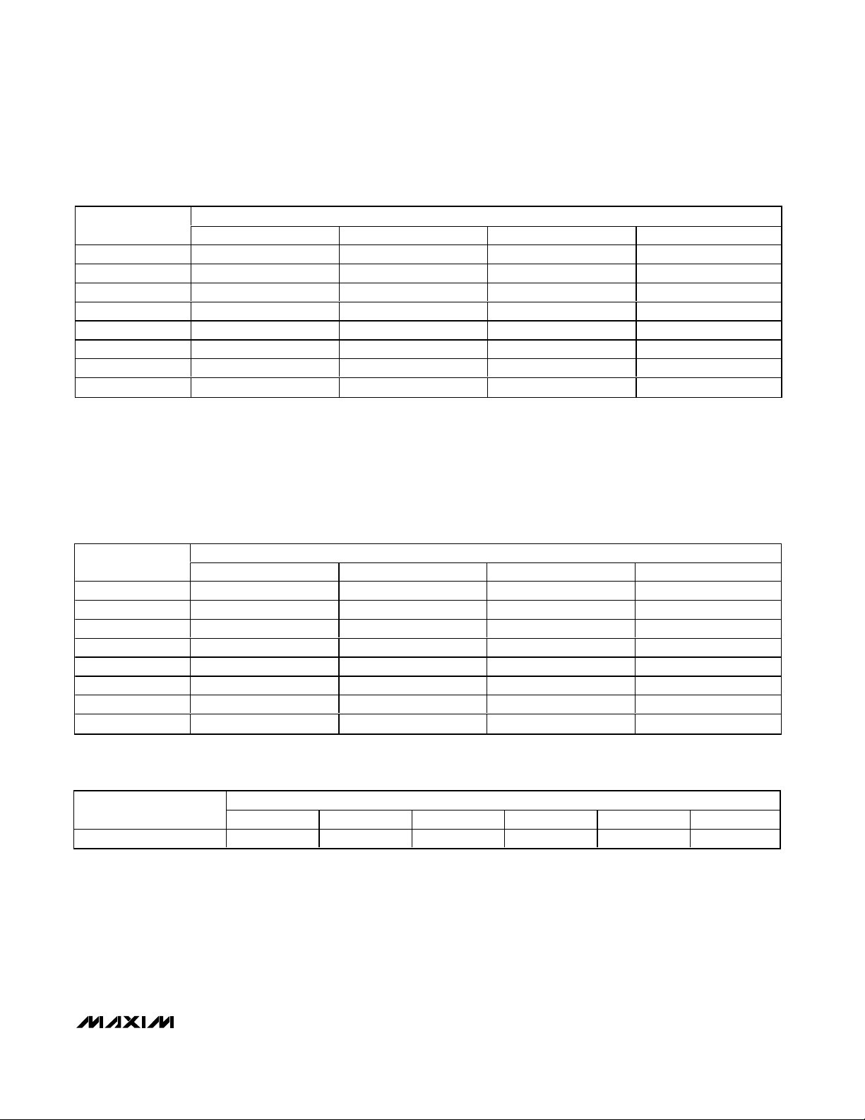
OUTPUT NOISE (µV
RMS
)
RATE (sps)
GAIN = 1 GAIN = 2 GAIN = 4 GAIN = 8
10 1.820 3.286 1.345 0.660
40 3.845 3.257 1.928 0.630
50 3.065 2.317 1.631 0.625
60 2.873 2.662 1.519 0.728
200 4.525 2.910 1.397 0.519
240 6.502 2.954 1.596 0.629
400 5.300 80.068 1.686 0.436
512 119.078 282.959 281.056 28.470
Table 1. Output Noise (Notes 12, 13, and 14)
Note 12: V
REF
= ±1.25V, bipolar mode, VIN= 1.24912, PGA gain = 1, TA= +85°C.
Note 13: C
IN
= 5pF, op-amp noise is considered to be the same as the switching noise. The increase of the op amp’s noise contri-
bution is due to large input swing (0 to 3.6V).
Note 14: Assume ±3 sigma peak-to-peak variation; noise-free resolution means no code flicker at given bits’ LSB.
PEAK-TO-PEAK RESOLUTION (Bits)
RATE (sps)
GAIN = 1 GAIN = 2 GAIN = 4 GAIN = 8
10 16.7 14.8 15.1 15.1
40 15.6 14.8 14.6 15.2
50 15.9 15.3 14.8 15.2
60 16.0 15.1 14.9 15.0
200 15.4 15.0 15.0 15.5
240 14.8 15.0 14.9 15.2
400 15.1 10.2 14.8 15.7
512 10.6 8.4 7.4 9.7
Table 2. Peak-to-Peak Resolution
EXTERNAL CAPACITANCE (pF)
PARAMETER
0 (Note 15) 50 100 500 1000 5000
Resistance (kΩ) 350 60 30 10 4 1
Table 3. Maximum External Source Impedance Without 16-Bit Gain Error
Note 15: 2pF parasitic capacitance is assumed, which represents pad and any other parasitic capacitance.
Page 12
MAX1358/MAX1359/MAX1360
16-Bit Data-Acquisition Systems with ADC, DACs,
UPIOs, RTC, Voltage Monitors, and Temp Sensor
12 ______________________________________________________________________________________
TIMING CHARACTERISTICS (Figures 1 and 21)
(AV
DD
= DVDD= +1.8V to +3.6V, external V
REF
= +1.25V, CLK32K = 32.768kHz (external clock), C
REG
= 10µF, C
CPOUT
= 10µF,
10µF between CF+ and CF-, T
A
= T
MIN
to T
MAX
, unless otherwise noted. Typical values are at TA= +25°C.) (Note 1)
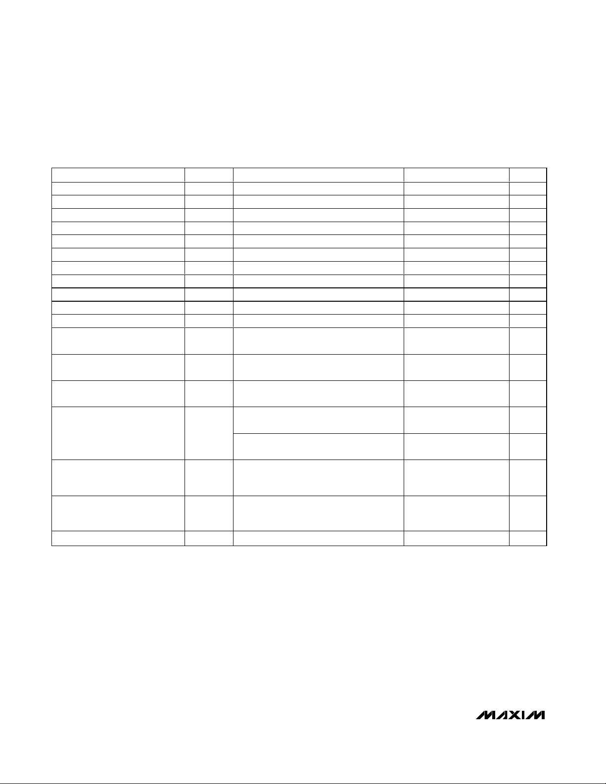
PARAMETER
CONDITIONS
UNITS
SCLK Operating Frequency f
SCLK
010
MHz
SCLK Cycle Time t
CYC
ns
SCLK Pulse-Width High t
CH
40 ns
SCLK Pulse-Width Low t
CL
40 ns
DIN to SCLK Setup t
DS
30 ns
DIN to SCLK Hold t
DH
0ns
SCLK Fall to DOUT Valid t
DO
CL = 50pF, Figure 2 40 ns
CS Fall to Output Enable t
DV
CL = 50pF, Figure 2 48 ns
CS Rise to DOUT Disable t
TR
CL = 50pF, Figure 2 48 ns
CS to SCLK Rise Setup t
CSS
20 ns
CS to SCLK Rise Hold t
CSH
0ns
DVDD Monitor Timeout Period
t
DSLP
(Note 16) 1.5 s
Wake-Up (WU) Pulse Width
t
WU
Minimum pulse width required to detect a
wake-up event
1µs
Shutdown Delay
t
DPU
The delay for SHDN to go high after a valid
wake-up event
1µs
The turn-on time for the high-frequency
clock and FLL (FLLE = 1) (Note 17)
10 ms
HFCK Turn-On Time
t
DFON
If FLLE = 0, the turn-on time for the highfrequency clock (Note 18)
10 µs
CRDY to INT Delay
t
DFI
The delay for CRDY to go low after the
HFCK clock output has been enabled
(Note 19)
ms
HFCK Disable Delay
t
DFOF
The delay after a shutdown command has
asserted and before HFCK is disabled
(Note 20)
ms
SHDN Assertion Delay
t
DPD
(Note 21)
ms
Note 16: The delay for the sleep voltage monitor output, RESET, to go high after VDDrises above the reset threshold. This is largely
driven by the startup of the 32kHz oscillator.
Note 17: It is gated by an AND function with three inputs—the external RESET signal, the internal DV
DD
monitor output, and the
external SHDN signal. The time delay is timed from the internal LOV
DD
going high or the external RESET going high,
whichever happens later. HFCK always starts in the low state.
Note 18: If FLLE = 0, the internal signal CRDY is not generated by the FLL block and INT or INT are deasserted.
Note 19: CRDY is used as an interrupt signal to inform the µC that the high-frequency clock has started. Only valid if FLLE = 1.
Note 20:
t
DFOF
gives the µC time to clean up and go into sleep-override mode properly.
Note 21:
t
DPD
is greater than the HFCK delay for the MAX1358/MAX1359/MAX1360 chip to clean up before losing power.
SYMBOL
MIN TYP MAX
100
7.82
1.95
2.93
Page 13
MAX1358/MAX1359/MAX1360
16-Bit Data-Acquisition Systems with ADC, DACs,
UPIOs, RTC, Voltage Monitors, and Temp Sensor
______________________________________________________________________________________ 13
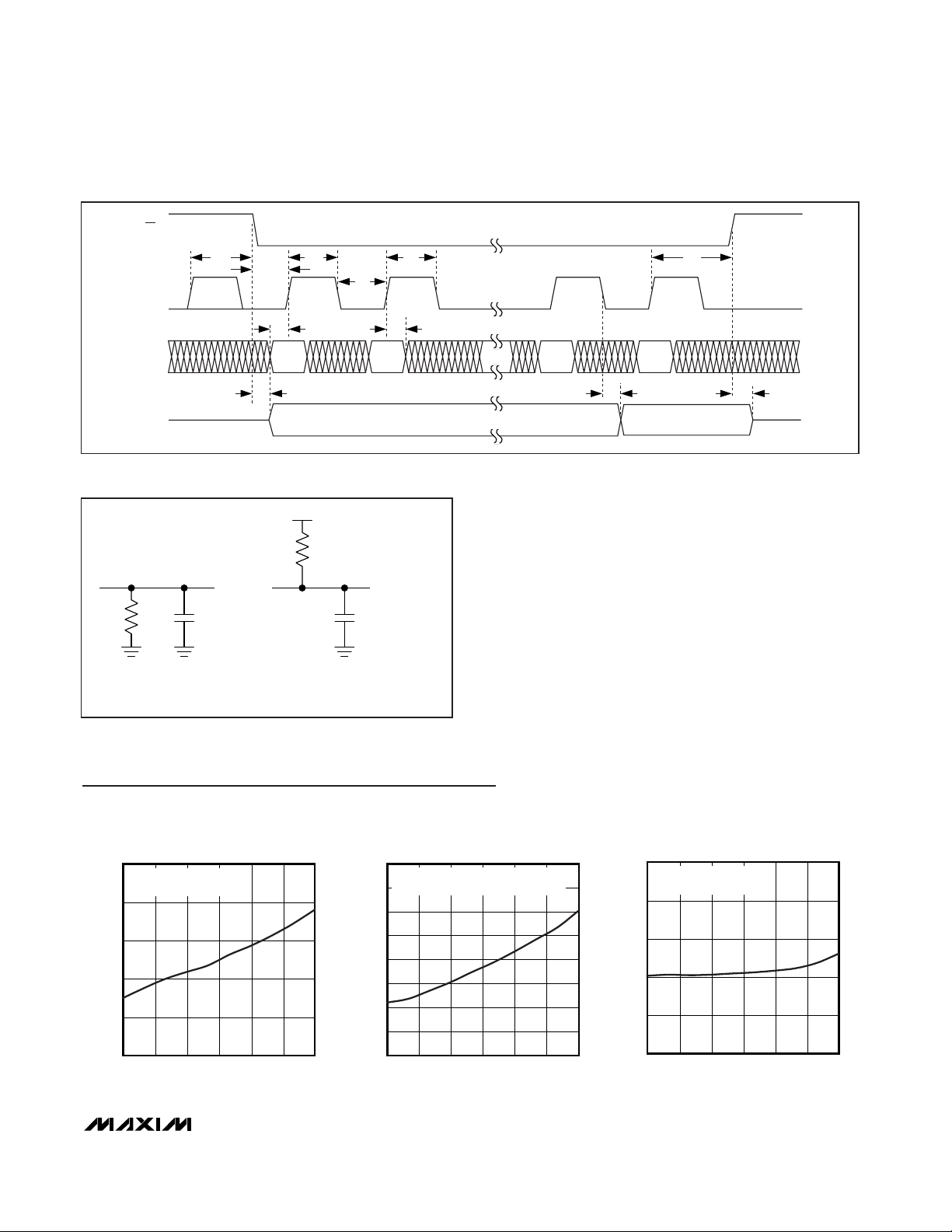
t
DS
t
CSS
t
DH
t
DV
t
DO
t
TR
CS
SCLK
DIN
DOUT
t
CSH
t
CYC
t
CH
t
CL
t
CSH
Figure 1. Detailed Serial-Interface Timing
DV
DD
C
LOAD
= 50pF
6kΩ
DOUT
a) FOR ENABLE, HIGH IMPEDANCE
TO V
OH
AND VOL TO V
OH
FOR DISABLE, VOH TO HIGH IMPEDANCE
b) FOR ENABLE, HIGH IMPEDANCE
TO V
OL
AND VOH TO V
OL
FOR DISABLE, VOL TO HIGH IMPEDANCE
DOUT
6kΩ
C
LOAD
= 50pF
Figure 2. DOUT Enable and Disable Time Load Circuits
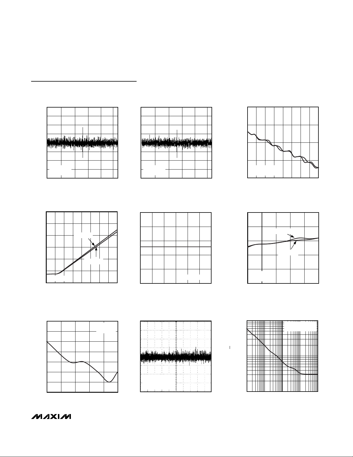
Typical Operating Characteristics
(DVDD= AV
DD
= 1.8V, REF = +1.25V C
CPOUT
= 10µF, TA= +25°C, unless otherwise noted.)
200
300
500
400
600
700
1.8 2.42.1 2.7 3.0 3.3 3.6
DVDD SUPPLY CURRENT
vs. DV
DD
SUPPLY VOLTAGE
MAX1358/59/60 toc01
DVDD (V)
SUPPLY CURRENT (µA)
NORMAL MODE
CLK BUFFER DISABLED
0
0.5
1.0
1.5
2.0
2.5
3.0
3.5
4.0
1.8 2.42.1 2.7 3.0 3.3 3.6
MAX1358/59/60 toc02
DVDD (V)
SUPPLY CURRENT (µA)
DVDD SUPPLY CURRENT
vs. DV
DD
SUPPLY VOLTAGE
SLEEP MODE, CLK BUFFER DISABLED
32kHz OSC, RTC, DV
DD
MONITOR ENABLED
0
0.2
0.6
0.4
0.8
1.0
1.8 2.42.1 2.7 3.0 3.3 3.6
MAX1358/59/60 toc03
DVDD (V)
SUPPLY CURRENT (µA)
DVDD SUPPLY CURRENT
vs. DV
DD
SUPPLY VOLTAGE
SLEEP MODE,
ALL FUNCTIONS DISABLED
Page 14
MAX1358/MAX1359/MAX1360
16-Bit Data-Acquisition Systems with ADC, DACs,
UPIOs, RTC, Voltage Monitors, and Temp Sensor
14 ______________________________________________________________________________________
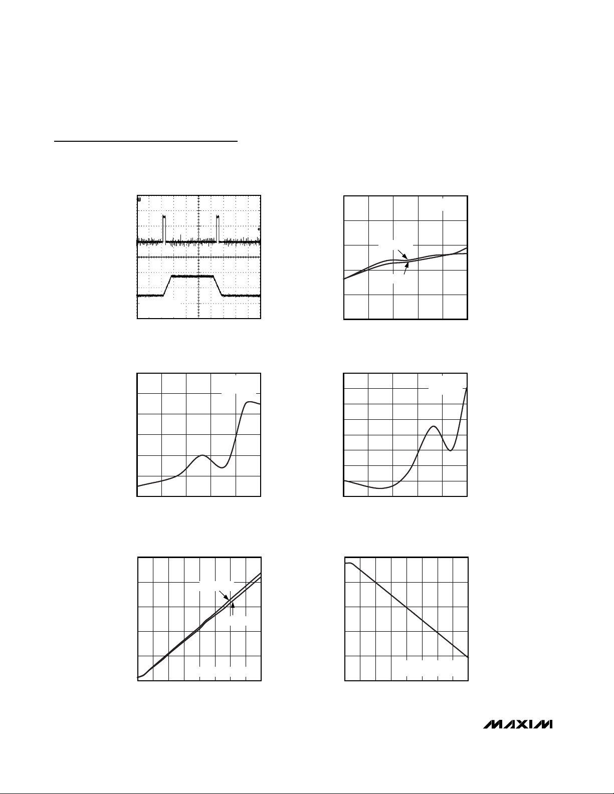
Typical Operating Characteristics (continued)
(DVDD= AV
DD
= 1.8V, REF = +1.25V C
CPOUT
= 10µF, TA= +25°C, unless otherwise noted.)
DVDD SUPPLY CURRENT
vs. TEMPERATURE
MAX1358/59/60 toc04
TEMPERATURE (°C)
SUPPLY CURRENT (µA)
603510-15
300
400
500
600
700
200
-40 85
DVDD = 3.0V
NORMAL MODE
CLK BUFFER DISABLED
DVDD = 1.8V
0
1.0
0.5
2.0
1.5
2.5
3.0
-40 10-15 35 60 85
MAX1358/59/60 toc05
TEMPERATURE (°C)
SUPPLY CURRENT (µA)
DVDD SUPPLY CURRENT
vs. TEMPERATURE
SLEEP MODE, CLK BUFFER DISABLED
32kHz OSC, RTC, DV
DD
MONITOR ENABLED
DVDD = 3.0V
DVDD = 1.8V
DVDD SUPPLY CURRENT
vs. TEMPERATURE
MAX1358/59/60 toc06
TEMPERATURE (°C)
SUPPLY CURRENT (µA)
603510-15
0.2
0.4
0.6
0.8
1.0
0
-40 85
DVDD = 3.0V
SLEEP MODE, ALL
FUNCTIONS DISABLED
DVDD = 1.8V
250
275
300
325
350
375
400
425
450
1.8 2.42.1 2.7 3.0 3.3 3.6
MAX1358/59/60 toc07
AVDD (V)
SUPPLY CURRENT (µA)
AVDD SUPPLY CURRENT
vs. AV
DD
SUPPLY VOLTAGE
NORMAL MODE
1.5
2.0
3.0
2.5
3.5
4.0
1.8 2.42.1 2.7 3.0 3.3 3.6
AVDD SUPPLY CURRENT
vs. AV
DD
SUPPLY VOLTAGE
MAX1358/59/60 toc08
AVDD (V)
SUPPLY CURRENT (µA)
SLEEP MODE,
32kHz OSC, RTC, DV
DD
MONITOR ENABLED
1.0
1.2
1.6
1.4
1.8
2.0
1.8 2.42.1 2.7 3.0 3.3 3.6
AVDD SUPPLY CURRENT
vs. AV
DD
SUPPLY VOLTAGE
MAX1358/59/60 toc09
AVDD (V)
SUPPLY CURRENT (µA)
SLEEP MODE,
ALL FUNCTIONS DISABLED
200
225
250
275
300
325
350
375
400
-40 -15 10 35 60 85
MAX1358/59/60 toc10
TEMPERATURE (°C)
SUPPLY CURRENT (µA)
NORMAL MODE
AVDD SUPPLY CURRENT
vs. TEMPERATURE
AVDD = 3.0V
AVDD = 1.8V
1.0
2.0
1.5
3.0
2.5
3.5
4.0
-40 10-15 35 60 85
MAX1358/59/60 toc11
TEMPERATURE (°C)
SUPPLY CURRENT (µA)
AVDD SUPPLY CURRENT
vs. TEMPERATURE
AVDD = 3.0V
AVDD = 1.8V
SLEEP MODE,
32kHz OSC, RTC, DV
DD
MONITOR ENABLED
AVDD SUPPLY CURRENT
vs. TEMPERATURE
MAX1358/59/60 toc12
TEMPERATURE (°C)
SUPPLY CURRENT (µA)
603510-15
1.2
1.4
1.6
1.8
2.0
1.0
-40 85
AVDD = 3.0V
SLEEP MODE, ALL
FUNCTIONS DISABLED
AVDD = 1.8V
Page 15
MAX1358/MAX1359/MAX1360
16-Bit Data-Acquisition Systems with ADC, DACs,
UPIOs, RTC, Voltage Monitors, and Temp Sensor
______________________________________________________________________________________ 15
Typical Operating Characteristics (continued)
(DVDD= AV
DD
= 1.8V, REF = +1.25V C
CPOUT
= 10µF, TA= +25°C, unless otherwise noted.)
2.1
2.3
2.2
2.5
2.4
2.7
2.6
2.8
-40 10-15 35 60 85
INTERNAL OSCILLATOR FREQUENCY
vs. TEMPERATURE
MAX1358/59/60 toc13
TEMPERATURE (°C)
INTERNAL OSCILLATOR FREQUENCY (MHz)
C
A: FLL DISABLED; AVDD, DVDD = 1.8V
B: FLL ENABLED
C: FLL DISABLED; AV
DD
, DVDD = 3.0V
B
A
CLK = 2.4576MHz
2.20
2.25
2.30
2.35
2.40
2.45
2.50
2.55
2.60
1.8 2.42.1 2.7 3.0 3.3 3.6
INTERNAL OSCILLATOR FREQUENCY
vs. SUPPLY VOLTAGE
MAX1358/59/60 toc14
AVDD, DVDD (V)
INTERNAL OSCILLATOR FREQUENCY (MHz)
FLL ENABLED
CLK = 2.4576MHz
FLL DISABLED
3.0
2.5
2.0
1.5
1.0
1.8 2.72.1 2.4 3.0 3.3 3.6
REFERENCE OUTPUT VOLTAGE
vs. SUPPLY VOLTAGE
MAX1358/59/60 toc15
AVDD (V)
REFERENCE OUTPUT VOLTAGE (V)
C
B
A
A: V
REF
= 1.25V
B: V
REF
= 2.048V
C: V
REF
= 2.5V
1.2510
1.2505
1.2500
1.2495
1.2490
-50 25050 150 350 450
REFERENCE OUTPUT VOLTAGE
vs. OUTPUT CURRENT
MAX1358/59/60 toc16
OUTPUT CURRENT (µA)
V
REF
(V)
AVDD = 1.8V
V
REF
= 1.25V
2.0472
2.0476
2.0474
2.0480
2.0478
2.0484
2.0482
2.0486
REFERENCE OUTPUT VOLTAGE
vs. OUTPUT CURRENT
MAX1358/59/60 toc17
V
REF
(V)
AVDD = 2.5V
V
REF
= 2.048V
-50 25050 150 350 450
OUTPUT CURRENT (µA)
2.5030
2.5036
2.5034
2.5032
2.5038
2.5040
2.5042
2.5044
2.5046
2.5048
2.5050
MAX1358/59/60 toc18
V
REF
(V)
-50 25050 150 350 450
OUTPUT CURRENT (µA)
AVDD = 3.0V
V
REF
= 2.5V
REFERENCE OUTPUT VOLTAGE
vs. OUTPUT CURRENT
0.9970
0.9975
0.9980
0.9985
0.9990
0.9995
1.0000
1.0005
1.0010
-40 -15 10 35 60 85
NORMALIZED REFERENCE OUTPUT
VOLTAGE vs. TEMPERATURE
MAX1358/59/60 toc19
TEMPERATURE (°C)
NORMALIZED REFERENCE VOLTAGE (V)
V
REF
= 1.25V
0.9970
0.9975
0.9980
0.9985
0.9990
0.9995
1.0000
1.0005
1.0010
-40 -15 10 35 60 85
NORMALIZED REFERENCE OUTPUT
VOLTAGE vs. TEMPERATURE
MAX1358/59/60 toc20
TEMPERATURE (°C)
NORMALIZED REFERENCE VOLTAGE (V)
V
REF
= 2.048V
0.9970
0.9975
0.9980
0.9985
0.9990
0.9995
1.0000
1.0005
1.0010
-40 -15 10 35 60 85
NORMALIZED REFERENCE OUTPUT
VOLTAGE vs. TEMPERATURE
MAX1358/59/60 toc21
TEMPERATURE (°C)
NORMALIZED REFERENCE VOLTAGE (V)
V
REF
= 2.5V
Page 16
MAX1358/MAX1359/MAX1360
16-Bit Data-Acquisition Systems with ADC, DACs,
UPIOs, RTC, Voltage Monitors, and Temp Sensor
16 ______________________________________________________________________________________
Typical Operating Characteristics (continued)
(DVDD= AV
DD
= 1.8V, REF = +1.25V C
CPOUT
= 10µF, TA= +25°C, unless otherwise noted.)
1s/div
REFERENCE VOLTAGE OUTPUT NOISE
(0.1Hz TO 10Hz)
50µV/div
MAX1358/59/60 toc22
V
REF
= +1.25V
AV
DD
= +1.8V
REFERENCE VOLTAGE OUTPUT
NOISE vs. FREQUENCY
MAX1358/59/60 toc23
FREQUENCY (Hz)
1k10010
1000
1
10k
10,000
100
V
REF
= 1.25V
NOISE (nV/√Hz)
REFERENCE VOLTAGE OUTPUT
NOISE vs. FREQUENCY
MAX1358/59/60 toc24
FREQUENCY (Hz)
1k10010
1000
1
10k
10,000
100
V
REF
= 2.048V
NOISE (nV/√Hz)
REFERENCE VOLTAGE OUTPUT
NOISE vs. FREQUENCY
MAX1358/59/60 toc25
FREQUENCY (Hz)
1k10010
1000
1
10k
10,000
100
V
REF
= 2.5V
NOISE (nV/√Hz)
-12
-8
-10
-4
-6
0
-2
2
-40 10-15 35 60 85
ADC MUX INPUT DC CURRENT
vs. TEMPERATURE
MAX1358/59/60 toc26
TEMPERATURE (°C)
INPUT CURRENT (µA)
AVDD = 1.8V
V
AIN
= 0.5V
-0.25
-0.15
0.05
-0.05
0.15
0.25
0400200 600 800 1000
DAC INL vs. OUTPUT CODE
MAX1358/59/60 toc27
OUTPUT CODE
INL (LSB)
AVDD = 1.8V
V
REF
= 1.25V
-0.25
-0.15
0.05
-0.05
0.15
0.25
0 400200 600 800 1000
DAC INL vs. OUTPUT CODE
MAX1358/59/60 toc28
OUTPUT CODE
INL (LSB)
AVDD = 2.5V
V
REF
= 2.048V
-0.25
-0.15
0.05
-0.05
0.15
0.25
0 400200 600 800 1000
DAC INL vs. OUTPUT CODE
MAX1358/59/60 toc29
OUTPUT CODE
INL (LSB)
AVDD = 3.0V
V
REF
= 2.5V
-0.20
-0.15
-0.10
-0.05
0
0.05
0.10
0.15
0.20
0400200 600 800 1000
DAC DNL vs. OUTPUT CODE
MAX1358/59/60 toc30
OUTPUT CODE
DNL (LSB)
AVDD = 1.8V
V
REF
= 1.25V
Page 17
MAX1358/MAX1359/MAX1360
16-Bit Data-Acquisition Systems with ADC, DACs,
UPIOs, RTC, Voltage Monitors, and Temp Sensor
______________________________________________________________________________________ 17
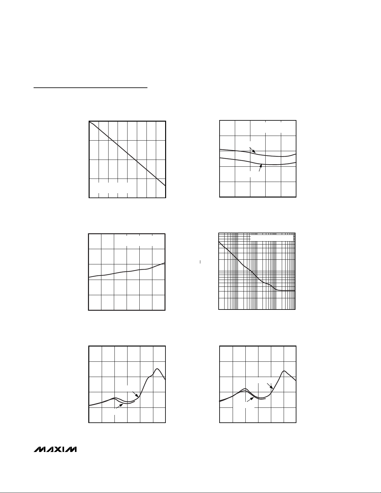
Typical Operating Characteristics (continued)
(DVDD= AV
DD
= 1.8V, REF = +1.25V C
CPOUT
= 10µF, TA= +25°C, unless otherwise noted.)
-0.20
-0.15
-0.10
-0.05
0
0.05
0.10
0.15
0.20
0 400200 600 800 1000
DAC DNL vs. OUTPUT CODE
MAX1358/59/60 toc31
OUTPUT CODE
DNL (LSB)
AVDD = 2.5V
V
REF
= 2.048V
-0.20
-0.15
-0.10
-0.05
0
0.05
0.10
0.15
0.20
0400200 600 800 1000
DAC DNL vs. OUTPUT CODE
MAX1358/59/60 toc32
OUTPUT CODE
DNL (LSB)
AVDD = 3.0V
V
REF
= 2.5V
1.240
1.242
1.244
1.246
1.248
00.501.00 1.500.25 0.75 1.25 1.75 2.00
DAC OUTPUT VOLTAGE
vs. OUTPUT SOURCE CURRENT
MAX1358/59/60 toc33
SOURCE CURRENT (mA)
DAC OUTPUT VOLTAGE (V)
CODE = 3FF hex
AV
DD
= 1.8V, 3.0V
0
0.05
0.10
0.15
0.20
0.25
0.30
DAC OUTPUT VOLTAGE
vs. OUTPUT SINK CURRENT
MAX1358/59/60 toc34
DAC OUTPUT VOLTAGE (V)
00.501.00 1.500.25 0.75 1.25 1.75 2.00
SOURCE CURRENT (mA)
CODE = 020 hex
AVDD = 1.8V
AVDD = 3.0V
650
640
630
610
600
1.8 2.72.1 2.4 3.0 3.3 3.6
DAC OUTPUT VOLTAGE
vs. ANALOG SUPPLY VOLTAGE
MAX1358/59/60 toc35
AVDD (V)
DAC OUTPUT VOLTAGE (mV)
CODE = 200 hex
620
620
622
626
624
628
630
-40 10-15 35 60 85
DAC OUTPUT VOLTAGE
vs. TEMPERATURE
MAX1358/59/60 toc36
TEMPERATURE (°C)
DAC OUTPUT VOLTAGE (mV)
AVDD = 3.0V
AVDD = 1.8V
V
REF
= 1.25V
CODE = 200 hex
-5
-3
-4
-1
-2
1
0
2
-40 10-15 35 60 85
DAC FBA/B INPUT BIAS CURRENT
vs. TEMPERATURE
MAX1358/59/60 toc37
TEMPERATURE (°C)
INPUT BIAS CURRENT (µA)
AVDD = 1.8V
V
AIN
= 0.5V
1s/div
DAC OUTPUT NOISE
(0.1Hz TO 10Hz)
50µV/div
MAX1358/59/60 toc38
AVDD = +1.8V
V
REF
= +1.25V
DAC CODE = 3FF hex
DAC OUTPUT
NOISE vs. FREQUENCY
MAX1358/59/60 toc39
FREQUENCY (Hz)
1k10010
1000
1
10k
10,000
100
DAC CODE = 3FF hex
V
REF
= 2.5V
NOISE (nV/√Hz)
Page 18
MAX1358/MAX1359/MAX1360
16-Bit Data-Acquisition Systems with ADC, DACs,
UPIOs, RTC, Voltage Monitors, and Temp Sensor
18 ______________________________________________________________________________________
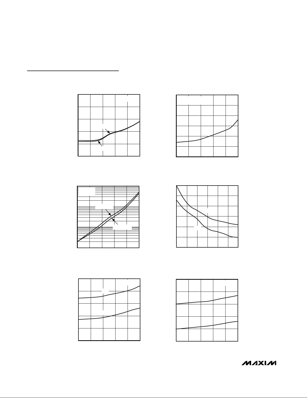
Typical Operating Characteristics (continued)
(DVDD= AV
DD
= 1.8V, REF = +1.25V C
CPOUT
= 10µF, TA= +25°C, unless otherwise noted.)
40µs/div
DAC LARGE-SIGNAL OUTPUT
STEP RESPONSE
MAX1358/59/60 toc40
V
REF
= +1.25V
AV
DD
= +3.0V
CS
2V/div
OUT_
1V/div
OP-AMP INPUT OFFSET VOLTAGE
vs. TEMPERATURE
MAX1358/59/60 toc41
TEMPERATURE (°C)
INPUT OFFSET VOLTAGE (mV)
603510-15
6.3
6.6
6.9
7.2
7.5
6.0
-40 85
AVDD = 1.8V
VCM = 0.5V
AVDD = 3.0V
0
4
2
8
6
10
12
-40 10-15 35 6085
MAX1358/59/60 toc42
TEMPERATURE (°C)
INPUT BIAS CURRENT (pA)
OP-AMP INPUT BIAS CURRENT
vs. TEMPERATURE
AVDD = 1.8V
V
CM
= 0.5V
-2
0
2
4
6
8
10
12
14
-40 -15 10 35 60 85
MAX1358/59/60 toc43
TEMPERATURE (°C)
INPUT BIAS CURRENT (pA)
OP-AMP INPUT BIAS CURRENT
vs. TEMPERATURE
AVDD = 3.0V
V
CM
= 0.5V
0
50
150
100
200
250
00.500.750.25 1.00 1.25 1.50 1.75 2.00
OP-AMP OUTPUT VOLTAGE
vs. OUTPUT SINK CURRENT
MAX1358/59/60 toc44
SINK CURRENT (mA)
OUTPUT VOLTAGE (mV)
UNITY GAIN, V
IN_
+ = 0V
AVDD = 1.8V
AVDD = 3.0V
2.80
2.84
2.92
2.88
2.96
3.00
00.500.750.25 1.00 1.25 1.50 1.75 2.00
OP-AMP OUTPUT VOLTAGE
vs. OUTPUT SOURCE CURRENT
MAX1358/59/60 toc45
SOURCE CURRENT (mA)
OUTPUT VOLTAGE (V)
AVDD = 3.0V
UNITY GAIN, V
IN_
+ = AV
DD
Page 19
MAX1358/MAX1359/MAX1360
16-Bit Data-Acquisition Systems with ADC, DACs,
UPIOs, RTC, Voltage Monitors, and Temp Sensor
______________________________________________________________________________________ 19
Typical Operating Characteristics (continued)
(DVDD= AV
DD
= 1.8V, REF = +1.25V C
CPOUT
= 10µF, TA= +25°C, unless otherwise noted.)
1.8 2.72.1 2.4 3.0 3.3 3.6
OP-AMP OUTPUT VOLTAGE
vs. AV
DD
SUPPLY VOLTAGE
MAX1358/59/60 toc48
AVDD (V)
OUTPUT VOLTAGE (mV)
500.2
500.4
500.6
500.8
501.0
500.0
UNITY GAIN, V
IN_
+ = 0.5V
R
L
= 10k
Ω
MAX1358/59/60 toc49
FREQUENCY (Hz)
1k10010
1000
1
10k
10,000
100
NOISE (nV/√Hz)
OP-AMP OUTPUT NOISE
vs. FREQUENCY
UNITY GAIN, V
IN_
+ = 0.5V
25
35
55
45
65
75
0 1.00.5 1.5 2.0 2.5 3.0
SPDT ON-RESISTANCE
vs. V
COM
VOLTAGE
MAX1358/59/60 toc50
V
COM
(V)
R
ON
(Ω)
AVDD = 3.0V
AVDD = 1.8V
50
70
110
90
130
150
01.00.5 1.5 2.0 2.5 3.0
SPST ON-RESISTANCE
vs. V
COM
VOLTAGE
MAX1358/59/60 toc51
V
COM
(V)
R
ON
(Ω)
AVDD = 3.0V
AVDD = 1.8V
1.60
1.65
1.70
1.75
1.80
OP-AMP OUTPUT VOLTAGE
vs. OUTPUT SOURCE CURRENT
MAX1358/59/60 toc46
OUTPUT VOLTAGE (V)
UNITY GAIN, V
IN_
+ = AV
DD
AV
DD
= 1.8V
00.500.750.25 1.00 1.25 1.50 1.75 2.00
SOURCE CURRENT (mA)
OP-AMP OUTPUT VOLTAGE
vs. TEMPERATURE
MAX1358/59/60 toc47
TEMPERATURE (°C)
OUTPUT VOLTAGE (mV)
603510-15
500.2
500.4
500.6
500.8
501.0
500.0
-40 85
AVDD = 1.8V
AVDD = 3.0V
UNITY GAIN, V
IN_
+ = 0.5V
R
L
= 10k
Ω
Page 20
MAX1358/MAX1359/MAX1360
16-Bit Data-Acquisition Systems with ADC, DACs,
UPIOs, RTC, Voltage Monitors, and Temp Sensor
20 ______________________________________________________________________________________
Typical Operating Characteristics (continued)
(DVDD= AV
DD
= 1.8V, REF = +1.25V C
CPOUT
= 10µF, TA= +25°C, unless otherwise noted.)
SPDT ON-RESISTANCE
vs. TEMPERATURE
MAX1358/59/60 toc52
TEMPERATURE (°C)
R
ON
(Ω)
603510-15
33
36
39
42
45
30
-40 85
AVDD = 3.0V
I
COM
= 1mA
AVDD = 1.8V
82
88
85
94
91
97
100
-40 10-15 35 60 85
MAX1358/59/60 toc53
TEMPERATURE (°C)
R
ON
(Ω)
SPST ON-RESISTANCE
vs. TEMPERATURE
AVDD = 1.8V, 3.0V
I
COM
= 1mA
SPDT/SPST ON/OFF-LEAKAGE
CURRENT vs. TEMPERATURE
MAX1358/59/60 toc54
TEMPERATURE (°C)
LEAKAGE CURRENT (pA)
603510-15
1
10
100
0.1
-40 85
ON-LEAKAGE
OFF-LEAKAGE
AVDD = 1.8V
V
CM
= 0V
15
25
20
35
30
40
45
1.8 2.4 2.72.1 3.0 3.3 3.6
SPDT/SPST SWITCHING TIME
vs. AV
DD
SUPPLY VOLTAGE
MAX1358/59/60 toc55
AVDD (V)
SWITCHING TIMES (ns)
t
ON
t
OFF
SPDT/SPST SWITCHING TIME
vs. TEMPERATURE
MAX1358/59/60 toc56
TEMPERATURE (°C)
SWITCHING TIMES (ns)
603510-15
34
38
42
46
50
30
-40 85
AVDD = 1.8V
t
ON
t
OFF
SPDT/SPST SWITCHING TIME
vs. TEMPERATURE
MAX1358/59/60 toc57
TEMPERATURE (°C)
SWITCHING TIMES (ns)
603510-15
19
23
27
31
35
15
-40 85
AVDD = 3.0V
t
ON
t
OFF
Page 21
MAX1358/MAX1359/MAX1360
16-Bit Data-Acquisition Systems with ADC, DACs,
UPIOs, RTC, Voltage Monitors, and Temp Sensor
______________________________________________________________________________________ 21
Typical Operating Characteristics (continued)
(DVDD= AV
DD
= 1.8V, REF = +1.25V C
CPOUT
= 10µF, TA= +25°C, unless otherwise noted.)
20µs/div
CHARGE-PUMP OUTPUT
VOLTAGE RIPPLE
MAX1358/59/60 toc63
DVDD = +1.8V
I
LOAD
= 10mA
CPOUT
20mV/div
AC-COUPLED
-0.20
-0.10
-0.15
0
-0.05
0.05
0.10
-40 10-15 35 6085
MAX1358/59/60 toc58
TEMPERATURE (°C)
% DEVIATION
VOLTAGE SUPERVISOR THRESHOLD
vs. TEMPERATURE
DVDD SUPERVISOR
CPOUT SUPERVISOR
3.0
3.2
3.1
3.4
3.3
3.5
3.6
0426810
CHARGE-PUMP OUTPUT VOLTAGE
vs. OUTPUT CURRENT
MAX1358/59/60 toc59
OUTPUT CURRENT (mA)
CPOUT VOLTAGE (V)
DVDD = 1.8V
3.10
3.14
3.22
3.18
3.26
3.30
-40 10-15 35 60 85
CHARGE-PUMP OUTPUT VOLTAGE
vs. TEMPERATURE
MAX1358/59/60 toc60
TEMPERATURE (°C)
CPOUT VOLTAGE (V)
DVDD = 3.0V
DVDD = 1.8V
I
OUT
= 10mA
0
20
60
40
80
100
084121620
CHARGE-PUMP OUTPUT RESISTANCE
vs. CAPACITANCE
MAX1358/59/60 toc61
CF (µF)
OUTPUT RESISTANCE (Ω)
DVDD = 1.8V
I
OUT
= 10mA
0
10
30
20
40
50
0426810
CHARGE-PUMP OUTPUT VOLTAGE
RIPPLE vs. OUTPUT CURRENT
MAX1358/59/60 toc62
OUTPUT CURRENT (mA)
OUTPUT VOLTAGE RIPPLE (mV)
DVDD = 1.8V
Page 22
MAX1358/MAX1359/MAX1360
16-Bit Data-Acquisition Systems with ADC, DACs,
UPIOs, RTC, Voltage Monitors, and Temp Sensor
22 ______________________________________________________________________________________
PIN
MAX1358
NAME FUNCTION
111CLK Clock Output. Default is 2.457MHz output clock for µC.
222UPIO2
User-Programmable Input/Output 2. See the UPIO2_CTRL Register section for
functionality.
333UPIO3
User-Programmable Input/Output 3. See the UPIO3_CTRL Register section for
functionality.
444UPIO4
User-Programmable Input/Output 4. See the UPIO4_CTRL Register section for
functionality.
555DOUT
Serial-Data Output. Data is clocked out on SCLK’s falling edge. High impedance
when CS is high, when UPIO/SPI passthrough mode is enabled, DOUT mirrors the
state of UPIO1.
666SCLK Serial-Clock Input. Clocks data in and out of the serial interface.
777DIN Serial-Data Input. Data is clocked in on SCLK’s rising edge.
888CS
Active-Low Chip-Select Input. Data is not clocked into DIN unless CS is low. When
CS is high, DOUT is high impedance. High impedance when CS is high, when
UPIO/SPI passthrough mode is enabled, DOUT mirrors the state of UPIO1.
999INT
Programmable Active-High/Low Interrupt Output. ADC, UPIO wake-up, alarm, and
voltage-monitor events.
10 10 10
32kHz Clock Input/Output. Outputs 32kHz clock for µC. Can be programmed as
an input by enabling the IO32E bit to accept an external 32kHz input clock. The
RTC, PWM, and watchdog timer always use the internal 32kHz clock derived from
the 32kHz crystal.
11 11 11
Active-Low Open-Drain Reset Output. Remains low while DVDD is below the 1.8V
voltage threshold and stays low for a timeout period (t
DSLP
) after DVDD rises above
the 1.8V threshold. RESET also pulses low when the watchdog timer times out and
holds low during POR until the 32kHz oscillator stabilizes.
12 12 12
32kHz Crystal Output. Connect external 32kHz watch crystal between 32KIN and
32KOUT.
13 13 13 32KIN
32kHz Crystal Input. Connect external 32kHz watch crystal between 32KIN and
32KOUT.
14 14 14 SNO1 Analog Switch 1 Normally Open Terminal. Analog input to mux.
15 15 15 SCM1 Analog Switch 1 Common Terminal. Analog input to mux.
16 16 16 SNC1 Analog Switch 1 Normally Closed Terminal. Analog input to mux (open on POR).
17 17 17 SNO2 Analog Switch 2 Normally Open Terminal. Analog input to mux.
18 18 18 SCM2 Analog Switch 2 Common Terminal. Analog input to mux (open on POR).
19 19 19 SNC2 Analog Switch 2 Normally Closed Terminal. Analog input to mux.
20 20 20 OUT1 Amplifier 1 Output. Analog input to mux.
21 21 21 IN1- Amplifier 1 Inverting Input. Analog input to mux.
22 22 22 IN1+ Amplifier 1 Noninverting Input
23 23 — SWA DACA SPST Shunt Switch Input. Connects to OUTA through a SPST switch.
24 24 — FBA DACA Force-Sense Feedback Input. Analog input to mux.
Pin Description
MAX1359 MAX1360
CLK32K
RESET
32KOUT
Page 23
MAX1358/MAX1359/MAX1360
16-Bit Data-Acquisition Systems with ADC, DACs,
UPIOs, RTC, Voltage Monitors, and Temp Sensor
______________________________________________________________________________________ 23
PIN
MAX1358
NAME FUNCTION
25 25 — OUTA DACA Force-Sense Output. Analog input to mux.
26 26 26 AGND Analog Ground
27 27 27 AV
DD
Analog Supply Voltage. Also ADC reference voltage during AVDD measurement.
Bypass to AGND with 10µF and 0.1µF capacitors in parallel as close to the pin as
possible.
28 — — SWB DACB SPST Shunt Switch Input. Connects to OUTB through an SPST switch.
29 — — FBB DACB Force-Sense Feedback Input. Analog input to mux.
30 — — OUTB Force-Sense DACB Ouput. Analog input to mux.
31 31 31 AIN2
Analog Input 2. Analog input to mux. Inputs have internal programmable current
source for external temperature measurement.
32 32 32 AIN1
Analog Input 1. Analog input to mux. Inputs have internal programmable current
source for external temperature measurement.
33 33 33 REF
Reference Input/Output. Output of the reference buffer amplifier or external
reference input. Disabled at power-up to allow external reference. Reference
voltage for ADC and DACs.
34 34 34 REG
Linear Voltage-Regulator Output. Charge-pump-doubler input voltage. Bypass
REG with a 10µF capacitor to DGND for charge-pump regulation.
35 35 35 CF-
36 36 36 CF+
Charge-Pump Flying Capacitor Terminals. Connect an external 10µF (typ)
capacitor between CF+ and CF-.
37 37 37
C har g e- P um p Outp ut. C onnect an exter nal 10µF ( typ ) r eser voi r cap aci tor b etw een
C P OU T and D G N D . Ther e i s a l ow thr eshol d d i od e b etw een D V
D D
and C P OU T. When
the char g e p um p i s d i sab l ed , C P OU T i s p ul l ed up w i thi n 300m V ( typ ) of D V
D D
.
38 38 38 DV
DD
Digital Supply Voltage. Bypass to DGND with 10µF and 0.1µF capacitors in parallel
as close to the pin as possible.
39 39 39 DGND
Digital Ground. Also ground for cascaded linear voltage regulator and chargepump doubler.
40 40 40 UPIO1 U ser - P r og r am m ab l e Inp ut/O utp ut 1. S ee the U P IO1_C TRL Reg i ster for functionality.
——23IN3+ Amplifier 3 Noninverting Input
——24IN3- Amplifier 3 Inverting Input. Analog input to mux.
——25OUT3 Amplifier 3 Output. Analog input to mux.
—2828IN2+ Amplifier 2 Noninverting Input
—2929IN2- Amplifier 2 Inverting Input. Analog input to mux.
—3030OUT2 Amplifier 2 Output. Analog input to mux.
———EPE xp osed P ad . Leave unconnected or connect to AGN D .
Pin Description (continued)
MAX1359 MAX1360
CPOUT
Page 24

MAX1358/MAX1359/MAX1360
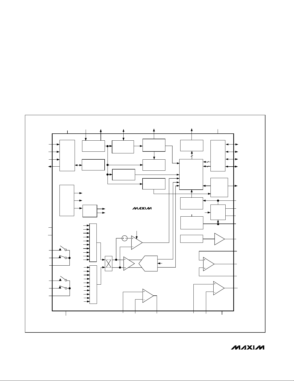
Detailed Description
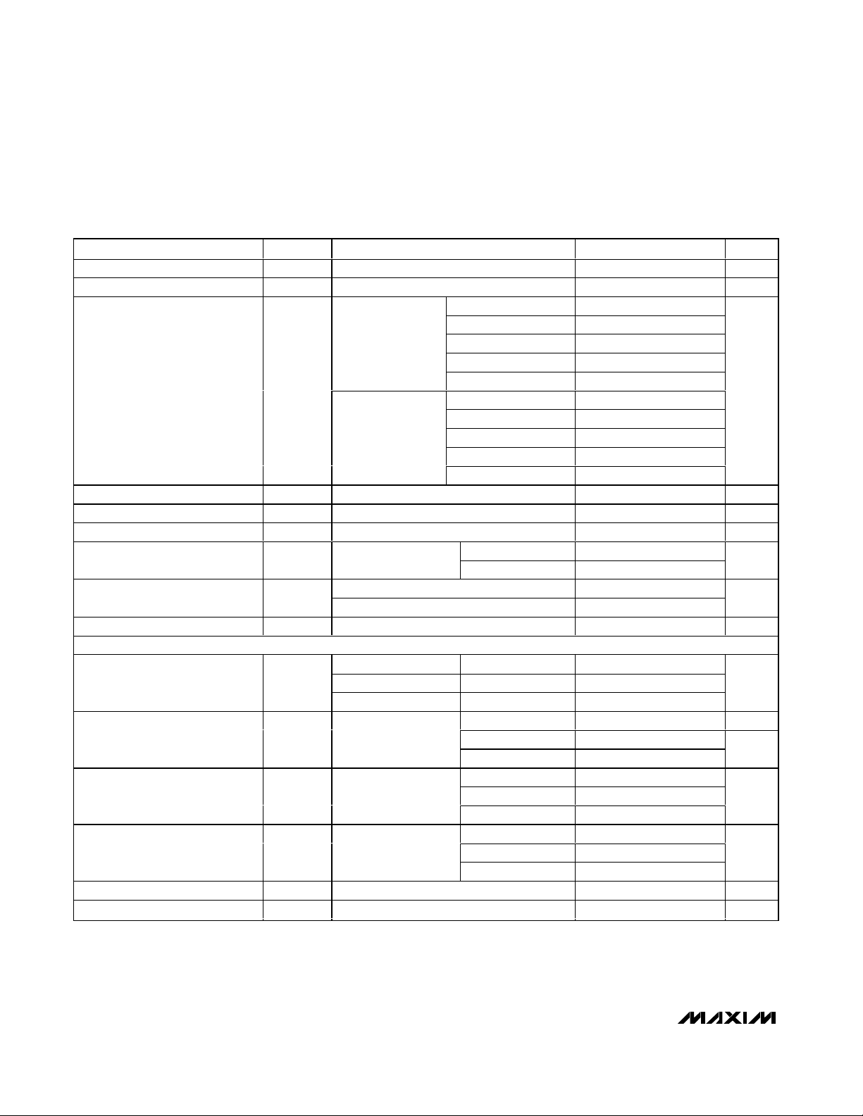
The MAX1358/MAX1359/MAX1360 DAS feature a multiplexed differential 16-bit ADC, 10-bit force-sense
DACs, an RTC with an alarm, a selectable bandgap
voltage reference, a signal-detect comparator, 1.8V
and 2.7V voltage monitors, and wake-up control
circuitry, all controlled by a 4-wire serial interface. (See
Figures 3, 4, and 5 for the functional diagrams).
The DAS directly interfaces to various sensor outputs
and, once configured, provides the stimulus, signal
conditioning, and data conversion, as well as µP support. See the Applications section for sample
MAX1358/MAX1359/MAX1360 applications.
The 16-bit ADC features programmable continuous conversion rates as shown in Table 4, and gains of 1, 2, 4,
and 8 (Table 5) to suit applications with different power
16-Bit Data-Acquisition Systems with ADC, DACs,
UPIOs, RTC, Voltage Monitors, and Temp Sensor
24 ______________________________________________________________________________________
TEMP
SENSOR
REF
AGND
OUTA
OUTB
SCM2
OUT1
AGND
REF
INM1
FBB
SCM1
FBA
AIN1
SNO1
SNC1
TEMP+
TEMP-
SNO2
SNC2
AIN2
10:1
MUX
NEG
10:1
MUX
POS
Av = 1, 2, 4, 8 V/V
POLARITY
FLIPPER
PROG. Vos
PGA
Av = 1, 1.6384, 2 V/V
UPIO
DGND AGND
AV
DD
DV
DD
SERIAL
INTERFACE
DIN
CS
DOUT
SCLK
1.25V BANDGAP
REF
16-BIT ADC
IN+
IN-
REF
OP1
10-BIT DAC
OUTA
REF
FBA
BUF
SWA
10-BIT DAC
OUTB
REF
FBB
BUF
SWB
PGA
OUT1
SNO1
SNC1
SCM1
CMP
UPIO1
UPIO2
UPIO3
UPIO4
32.768kHz
OSCILLATOR
32KIN
32KOUT
WATCHDOG
TIMER
4.9152MHz HF
OSCILLATOR
AND FLL
CLK
CLK32K
AIN2
AIN1
INTERRUPT
INT
PWM
CLK32K
INPUT/OUTPUT
CONTROL
DV
DD
(1.8V)
VOLTAGE
MONITOR
RTC AND
ALARM
SNO2
SNC2
SCM2
CHARGE-
PUMP
DOUBLER
CF+
CF-
IN1-IN1+
PROG
CURRENT
SOURCE
TEMP+
TEMP-
32K
AIN2
AIN1
CPOUT (2.7V)
VOLTAGE
MONITOR
LINEAR 1.65V
VOLTAGE
REGULATOR
CPOUT
REG
STATUS
4
RESET
LDVD
ALD
CRDY
SDC
ADD
ADOU
UPR<4:1>
4
UPF<4:1>
LCPD
16
CONTROL
LOGIC
HFCLK
M32K
M32K
M32K
HFCLK
WDTO
DV
DD
MAX1358
SPDT1
SPDT2
Figure 3. MAX1358 Functional Diagram
Page 25

and dynamic range constraints. The force-sense DACs
provide 10-bit resolution for precise sensor applications. The ADCs and DACs both utilize a low-drift 1.25V
internal bandgap reference for conversions and fullscale range setting. The RTC has a 138-year range and
provides an alarm function that can be used to wake up
the system or cause an interrupt at a predefined time.
The power-supply voltage monitor detects when DV
DD
falls below a trip threshold voltage of +1.8V, asserting
RESET. The MAX1358/MAX1359/MAX1360 use a 4-wire
serial interface to communicate directly between SPI,
QSPI, or MICROWIRE devices for system configuration
and readback functions.
Analog-to-Digital Converter (ADC)
The MAX1358/MAX1359/MAX1360 include a sigmadelta ADC with programmable conversion rate, a PGA,
and a dual 10:1 input mux. When performing continu-
MAX1358/MAX1359/MAX1360
16-Bit Data-Acquisition Systems with ADC, DACs,
UPIOs, RTC, Voltage Monitors, and Temp Sensor
______________________________________________________________________________________ 25
TEMP
SENSOR
REF
AGND
OUTA
OUT2
SCM2
OUT1
AGND
REF
INM1
IN2-
SCM1
FBA
AIN1
SNO1
SNC1
TEMP+
TEMP-
SNO2
SNC2
AIN2
10:1
MUX
NEG
10:1
MUX
POS
Av = 1, 2, 4, 8 V/V
POLARITY
FLIPPER
PROG. Vos
PGA
Av = 1, 1.6384, 2 V/V
UPIO
DGND
AGND
AV
DD
DV
DD
SERIAL
INTERFACE
DIN
CS
DOUT
SCLK
1.25V BANDGAP
REF
16-BIT ADC
IN+
IN-
REF
OP1
10-BIT DAC
OUTA
REF
FBA
BUF
SWA
PGA
OUT1
SNO1
SNC1
SCM1
CMP
UPIO1
UPIO2
UPIO3
UPIO4
32.768kHz
OSCILLATOR
32KIN
32KOUT
WATCHDOG
TIMER
4.9152MHz HF
OSCILLATOR
AND FLL
CLK
CLK32K
AIN2
AIN1
INTERRUPT
INT
PWM
CLK32K
INPUT/OUTPUT
CONTROL
DV
DD
(1.8V)
VOLTAGE
MONITOR
RTC AND
ALARM
SNO2
SNC2
SCM2
CHARGE-
PUMP
DOUBLER
CF+
CF-
IN1-IN1+
PROG
CURRENT
SOURCE
TEMP+
TEMP-
32K
AIN2
AIN1
CPOUT (2.7V)
VOLTAGE
MONITOR
LINEAR 1.65V
VOLTAGE
REGULATOR
CPOUT
REG
STATUS
4
RESET
LDVD
ALD
CRDY
SDC
ADD
ADOU
UPR<4:1>
4
UPF<4:1>
LCPD
16
CONTROL
LOGIC
HFCLK
M32K
M32K
M32K
HFCLK
WDTO
DV
DD
MAX1359
OP2
OUT2
IN2-IN2+
SPDT1
SPDT2
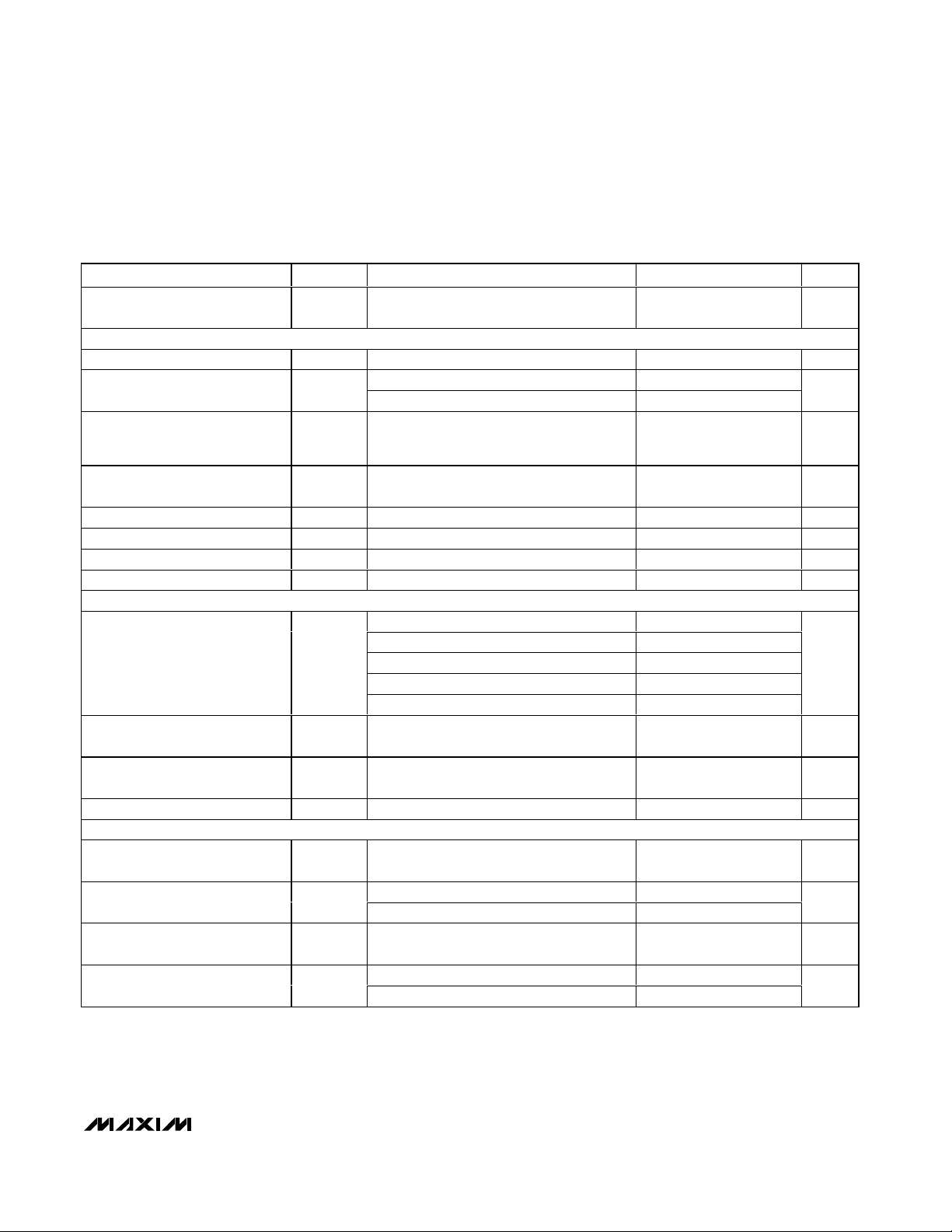
Figure 4. MAX1359 Functional Diagram
Page 26
MAX1358/MAX1359/MAX1360
ous conversions at 10sps or single conversions at the
40sps setting (effectively 10sps due to four sample
sigma-delta settling), the ADC has 16-bit noise-free resolution. The noise-free resolution drops to 10 bits at the
maximum sampling rate of 512sps. Differential inputs
support unipolar (between 0 and V
REF
) and bipolar
(between ±V
REF
) modes of operation. Note: Avoid
combinations of input signal and PGA gains that
exceed the reference range at the ADC input. The
ADOU bit in the status register indicates if the ADC has
over-ranged or under-ranged.
Zero-scale and full-scale calibrations remove offset and
gain errors. Direct access to gain and zero-scale calibration registers allows system-level offset and gain calibration. The zero-scale adjustment register allows
intentional positive offset skewing to preserve unipolarmode resolution for signals that have a slight negative
16-Bit Data-Acquisition Systems with ADC, DACs,
UPIOs, RTC, Voltage Monitors, and Temp Sensor
26 ______________________________________________________________________________________
TEMP
SENSOR
REF
AGND
OUT3
OUT2
SCM2
OUT1
AGND
REF
INM1
IN2-
SCM1
IN3-
AIN1
SNO1
SNC1
TEMP+
TEMP-
SNO2
SNC2
AIN2
10:1
MUX
NEG
10:1
MUX
POS
Av = 1, 2, 4, 8 V/V
POLARITY
FLIPPER
PROG. Vos
PGA
Av = 1, 1.6384, 2 V/V
UPIO
DGND
AGND
AV
DD
DV
DD
SERIAL
INTERFACE
DIN
CS
DOUT
SCLK
1.25V BANDGAP
REF
16-BIT ADC
IN+
IN-
REF
OP1
IN3+
IN3-
OP3
OUT3
PGA
OUT1
SNO1
SNC1
SCM1
CMP
UPIO1
UPIO2
UPIO3
UPIO4
32.768kHz
OSCILLATOR
32KIN
32KOUT
WATCHDOG
TIMER
4.9152MHz HF
OSCILLATOR
AND FLL
CLK
CLK32K
AIN2
AIN1
INTERRUPT
INT
PWM
CLK32K
INPUT/OUTPUT
CONTROL
DV
DD
(1.8V)
VOLTAGE
MONITOR
RTC AND
ALARM
SNO2
SNC2
SCM2
CHARGE-
PUMP
DOUBLER
CF+
CF-
IN1-IN1+
PROG
CURRENT
SOURCE
TEMP+
TEMP-
32K
AIN2
AIN1
CPOUT (2.7V)
VOLTAGE
MONITOR
LINEAR 1.65V
VOLTAGE
REGULATOR
CPOUT
REG
STATUS
4
RESET
LDVD
ALD
CRDY
SDC
ADD
ADOU
UPR<4:1>
4
UPF<4:1>
LCPD
16
CONTROL
LOGIC
HFCLK
M32K
M32K
M32K
HFCLK
WDTO
DV
DD
MAX1360
OP2
OUT2
IN2-IN2+
SPDT1
SPDT2
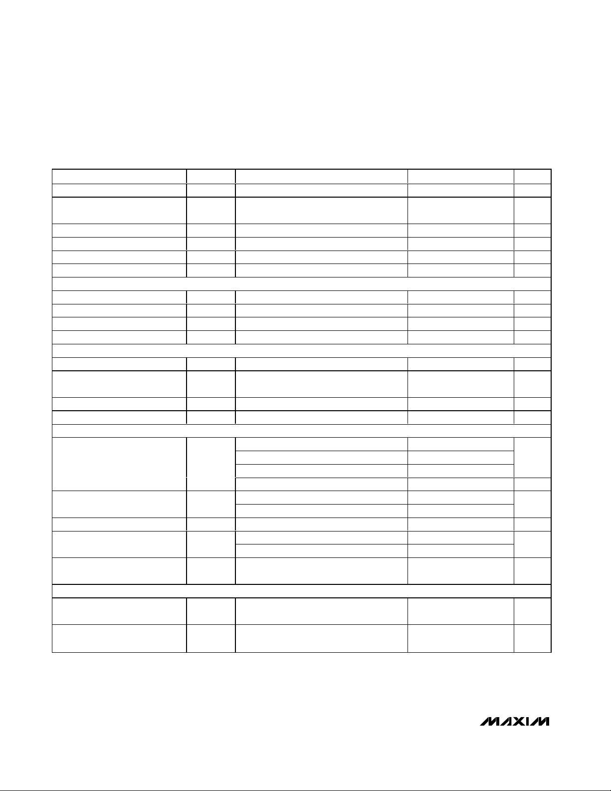
Figure 5. MAX1360 Functional Diagram
Page 27

offset (i.e., unipolar clipping near zero can be removed).
Perform ADC calibration whenever the ADC configuration, temperature, or AVDDchanges. The ADC-done status can be programmed to provide an interrupt on INT
or on any UPIO_.
PGA Gain
An integrated PGA provides four selectable gains: +1V/V,
+2V/V, +4V/V, and +8V/V to maximize the dynamic range
of the ADC. Bits GAIN1 and GAIN0 set the gain (see the
ADC Register for more information). The PGA gain is
implemented in the digital filter of the ADC.
ADC Modulator
The MAX1358/MAX1359/MAX1360 perform analog-todigital conversions using a single-bit, 3rd-order,
switched-capacitor sigma-delta modulator. The sigmadelta modulation converts the input signal into a digital
pulse train whose average duty cycle represents the digitized signal information. The pulse train is then
processed by a digital decimation filter. The modulator
provides 2nd-order frequency shaping of the quantization noise resulting from the single-bit quantizer. The
modulator is fully differential for maximum signal-to-noise
ratio and minimum susceptibility to power-supply noise.
Signal-Detect Comparator
INT asserts (and remains asserted) within 30µs when
the differential voltage on the selected analog inputs
exceeds the signal-detect comparator trip threshold.
The signal-detect comparator’s differential input trip
threshold (i.e., offset) is user selectable and can be programmed to the following values: 0mV, 50mV, 100mV,
150mV, or 200mV.
Analog Inputs
The ADC provides two external analog inputs: AIN1
and AIN2. The rail-to-rail inputs accept differential or
single-ended voltages, or external temperature-sensing
diodes. The unused op amps, switches, or DAC inputs
and output pins can also be used as rail-to-rail analog
inputs if the associated function is disabled.
Analog Input Protection
Internal protection diodes clamp the analog inputs to
AVDDand AGND, and allow the channel input to swing
from (AGND - 0.3V) to (AVDD+ 0.3V). For accurate
conversions near full scale, the inputs must not exceed
AVDDby more than 50mV or be lower than AGND by
50mV. If the inputs exceed (AGND - 0.3V) to (AVDD+
0.3V), limit the current to 50mA.
Analog Mux
The MAX1358/MAX1359/MAX1360 include a dual 10:1
mux for the positive and negative inputs of the ADC.
Figures 3, 4, and 5 illustrate which signals are present at
the inputs of each mux for the MAX1358/MAX1359/
MAX1360. The MUXP[3:0] and MUXN[3:0] bits of the mux
register select the input to the ADC and the signal-detect
comparator (Tables 8 and 9). See the mux register
description in the Register Definitions section for multiplexer functionality. The POL bit of the ADC register
swaps the polarity of mux output signals to the ADC.
Digital Filtering
The MAX1358/MAX1359/MAX1360 contain an on-chip
digital lowpass filter that processes the data stream
from the modulator using a SINC4(sinx/x)4response.
The SINC4filter has a settling time of four output data
periods (4 x 200ms).
The MAX1358/MAX1359/MAX1360 have 25% overrange
capability built into the modulator and digital filter:
Figure 6 shows the filter frequency response. The
SINC4characteristic -3dB cutoff frequency is 0.228
times the first notch frequency.
The output data rate for the digital filter corresponds
with the positioning of the first notch of the filter’s frequency response. The notches of the SINC
4
filter are
repeated at multiples of the first notch frequency. The
SINC4filter provides an attenuation of better than
100dB at these notches. For example, 50Hz is equal to
five times the first notch frequency and 60Hz is equal to
six times the first notch frequency.
Hf
N
SIN N
f
f
SIN
f
f
m
m
()=
1
4
π
π
MAX1358/MAX1359/MAX1360
16-Bit Data-Acquisition Systems with ADC, DACs,
UPIOs, RTC, Voltage Monitors, and Temp Sensor
______________________________________________________________________________________ 27
FREQUENCY (Hz)
GAIN (dB)
10080604020
-160
-120
-80
-40
0
-200
0120
Figure 6. Filter Frequency Response
Page 28
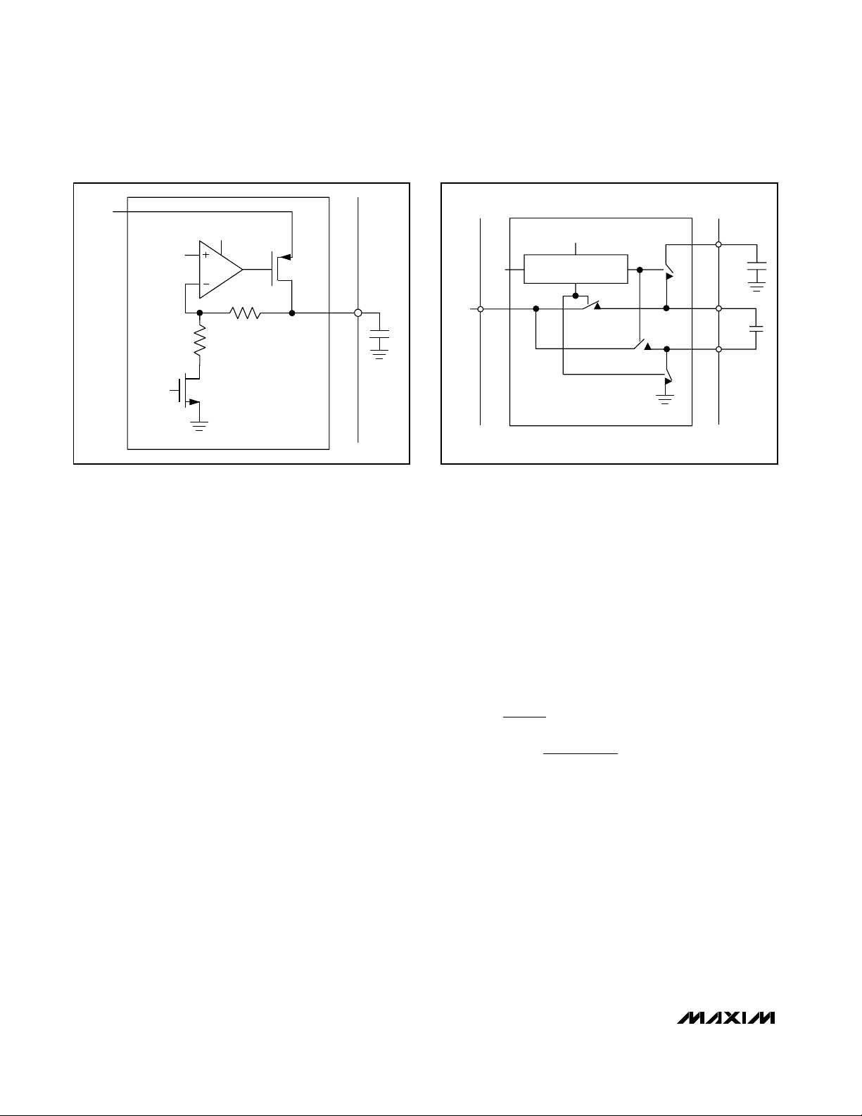
MAX1358/MAX1359/MAX1360
Force-Sense DAC (MAX1358/MAX1359)
The MAX1358 incorporates two 10-bit force-sense
DACs and the MAX1359 has one. The DACs’ reference
voltage sets the full-scale range. Program the
DACA_OP and DACB_OP registers using the serial
interface to set the output voltages of the DACs at
OUTA and OUTB. Shorting FBA/B and OUTA/B configures the DAC in a unity-gain setting. Connecting resistors in a voltage-divider configuration between
OUTA/B, FBA/B, and GND sets a different closed-loop
gain for the output amplifier (see the Applications
Information section).
The DAC output amplifier typically settles to ±0.5 LSB
from a full-scale transition within 50µs (unity gain and
loaded with 10kΩ in parallel with 200pF). Loads of less
than 1kΩ may degrade performance. See the Typical
Operating Characteristics for the source-and-sink
capability of the DAC output.
The MAX1358/MAX1359 feature a software-programmable shutdown mode for the DACs. Power down
DACA or DACB independently or simultaneously by
clearing the DAE and DBE bits (see the DACA_OP
Registers and DACB_OP Registers sections). DAC outputs OUTA and OUTB go high impedance when powered down. The DACs are normally powered down at
power-on reset.
Charge Pump
The charge pump provides >3V at CPOUT with a maximum 10mA load. Enable the charge pump through the
PS_VMONS register. The charge pump is powered
from DVDD. See Figures 7 and 8 for block diagrams of
the charge pump and linear regulator. The charge
pump is disabled at power-on reset.
An internal clock drives the charge-pump clock and
ADC clock. The charge pump delivers a maximum
10mA of current to external devices. The droop and the
ripple depend on the clock frequency (f
CLK
=
32.768kHz / 2), switch resistances (R
SWITCH
= 5Ω),
and the external capacitors (10µF) along with their
respective ESRs, as shown below.
Voltage Supervisors
The MAX1358/MAX1359/MAX1360 provide voltage
supervisors to monitor DVDDand CPOUT. The first
supervisor monitors the DVDDsupply voltage. RESET
asserts and sets the corresponding LDVD status bit
when DVDDfalls below the 1.8V threshold voltage. When
the DVDDsupply voltage rises above the threshold during power-up, RESET deasserts after a nominal 1.5s
timeout period to give the crystal oscillator time to stabilize. Set the threshold hysteresis using the HYSE bit of
the PS_VMONS register. See the PS_VMONS Register
section for configuring hysteresis. There is no separate
voltage monitor for AVDD, but the analog supply is cov-
VIR
R
fC
R ESR ESR
V
I
fC
I ESR
DROOP OUT OUT
OUT
CLK F
SWITCH C C
RIPPLE
OUT
CLK CPOUT
OUT C
F CPOUT
CPOUT
=
=+ ++
=+
1
24
2
16-Bit Data-Acquisition Systems with ADC, DACs,
UPIOs, RTC, Voltage Monitors, and Temp Sensor
28 ______________________________________________________________________________________
OP
1.22V
1.65V
LINEAR 1.65V VOLTAGE REGULATOR
DV
DD
REG
LDOE
LDOE
Figure 7. Linear-Regulator Block Diagram
CF+
CF-
CPOUT
REG
M32K
CHARGE-PUMP DOUBLER
NONOVERLAP
CLOCK GENERATOR
CPE
Figure 8. Charge-Pump Block Diagram
Page 29

ered by the DVDDmonitor in many applications where
DVDDand AVDDare externally connected together.
Multiple supply applications where AVDDand DVDDare
not connected together require a separate external voltage monitor for AVDD. See Figure 9 for a block diagram
of the DV
DD
voltage supervisor.
The second voltage monitor tracks the charge-pump
output voltage, CPOUT. If CPOUT falls below the 2.7V
threshold, a corresponding register status bit (LCPD) is
set to flag the condition. The CPOUT monitor output
can also be mapped to the interrupt generator and output on INT. The CPOUT monitor can be used as a 3V
AVDDmonitor in applications where the charge pump is
disabled and CPOUT is connected to AVDD. AV
DD
must be greater or equal to DVDDwhen CPOUT is used
to monitor AV
DD.
See Figure 10 for a block diagram of
the CPOUT voltage supervisor.
Interrupt Generator (INT)
The interrupt generator provides an interrupt to an
external µC. The source of the interrupt is generated by
the status register and can be masked and unmasked
through the IMSK register. CRDY is unmasked by
default and INT is active-high at power-on reset. INT is
programmable as active-high and active-low. Possible
sources include a rising or falling edge of UPIO_, an
RTC alarm, an ADC conversion completion, or the voltage-supervisor outputs. The interrupt causes INT to
assert when configured as an interrupt output.
Crystal Oscillator
The on-chip oscillator requires an external crystal (or
resonator) connected between 32KIN and 32KOUT
with a 32.768kHz operating frequency. This oscillator is
used for the RTC, alarm, PWM, watchdog, charge
pump, and FLL. In any crystal-based oscillator circuit,
the oscillator frequency is sensitive to the capacitive
load (CL). CLis the capacitance that the crystal needs
from the oscillator circuit and not the capacitance of the
crystal. The input capacitance across the 32KIN and
32KOUT is 6pF. Choose a crystal with a 32.768kHz
oscillation frequency and a 6pF capacitive load such
as the C-002RX32-E from Epson Crystal. Using a crystal with a CLthat is larger than the load capacitance of
the oscillator circuit causes the oscillator to run faster
than the specified nominal frequency of the crystal or to
not start up. See Figures 11 and 12 for block diagrams
of the crystal oscillator and the CLK32K I/O.
MAX1358/MAX1359/MAX1360
16-Bit Data-Acquisition Systems with ADC, DACs,
UPIOs, RTC, Voltage Monitors, and Temp Sensor
______________________________________________________________________________________ 29
CMP
ANALOG
2:1 MUX
CONTROL
LOGIC
RESET
DV
DD
1.25V
1.8VTH
2.0VTH
LDVD
LSDE
LSDE
HYSE
POR
RSTE
DV
DD
(1.8V) VOLTAGE MONITOR
WDTO
Figure 9. DVDDVoltage-Supervisor Block Diagram
CMP
CPOUT
1.25V
2.7VTH
LCPD
CPDE
CPDE
CPOUT (2.7V) VOLTAGE MONITOR
Figure 10. CPOUT Voltage-Supervisor Block Diagram
Page 30

MAX1358/MAX1359/MAX1360
16-Bit Data-Acquisition Systems with ADC, DACs,
UPIOs, RTC, Voltage Monitors, and Temp Sensor
30 ______________________________________________________________________________________
Real-Time Clock (RTC)
The integrated RTC provides the current time information
from a 32-bit counter and subsecond counts from an 8bit ripple counter. An internally generated reference
clock of 256Hz (derived from the 32.768kHz crystal) drives the 8-bit subsecond counter. An overflow of the 8-bit
subsecond counter inputs a 1Hz clock to increment the
32-bit second counter. The RTC 32-bit second counter is
translatable to calendar format with firmware. All 40 bits
(32-bit second counter and 8-bit subsecond counter)
must be clocked in or out for valid data. The RTC and
the 32.768kHz crystal oscillator consume less than 1µA
when the rest of the IC is powered down.
Time-of-Day Alarm
Program the AL_DAY register with a 20-bit value, which
corresponds to a time 1s to 12 days later than the cur-
rent time with a 1s resolution. The alarm status bit, ALD,
asserts when the 20 bits of the AL_DAY register matches the 20 LSBs of the 32-bit second counter. The ADE
bit automatically clears when the time-of-day alarm
trips. The time-of-day alarm causes the device to exit
sleep mode.
Watchdog
Enable the watchdog timer by writing a 1 to the WDE bit
in the CLK_CTRL register. After enabling the watchdog
timer, the device asserts RESET for 250ms, if the
watchdog address register is not written every 500ms.
Due to the asynchronous nature of the watchdog timer,
the watchdog timeout period varies between 500ms
and 750ms. Write a 0 to the WDE bit to disable the
watchdog timer. See Figure 13 for a block diagram of
the watchdog timer.
32KIN
32KOUT
32.768kHz OSCILLATOR
32kHz
OSCILLATOR
OSCE
32K
Figure 11. 32kHz Crystal-Oscillator Block Diagram
IO32E
CLK32K
CK32E
OSCE
CLK32K I/O CONTROL
2:1
MUX
1
0
IO32E
IO32E
32K
M32K
Figure 12. CLK32K I/O Block Diagram
D
Q
Q
R
CK
D
Q
Q
R
CK
DIVIDE-
BY-8192
32K
WDE
POR
WDW
WATCHDOG TIMER
POR PULSES HIGH DURING POWER-UP.
WDW PULSES HIGH DURING WATCHDOG REGISTER WRITE.
4Hz
WDTO
Figure 13. Watchdog Timer Block Diagram
Page 31

High-Frequency Clock
An internal oscillator and a frequency-locked loop (FLL)
are used to generate a 4.9152MHz ±1% high-frequency clock. This clock and derivatives are used internally
by the ADC, analog switches, and PWM. This clock signal outputs to CLK. When the FLL is enabled, the highfrequency clock is locked to the 32.768kHz reference. If
the FLL is disabled, the high-frequency clock is freerunning. At power-up, the CLK pin defaults to a
2.4576MHz clock output, which is compatible with most
µCs. See Figure 14 for a block diagram of the high-frequency clock.
User-Programmable I/Os
The MAX1358/MAX1359/MAX1360 provide four digital
programmable I/Os (UPIO1–UPIO4). Configure UPIOs
as logic inputs or outputs using the UPIO control register. Configure the internal pullups using the UPIO setup
register, if required. At power-up, the UPIO’s are internally pulled up to DVDD. UPIO_ outputs can be referenced to DVDDor CPOUT. See the UPIO__CTRL
Register and UPIO_SPI Register sections for more
details on configuring the UPIO_ pins.
Program each UPIO1–UPIO4 as one of the following:
• General-purpose input
• Power-mode control
• Analog switch (SPST) and SPDT control input
• ADC data-ready output
• General-purpose output
• PWM output
• Alarm output
• SPI passthrough
MAX1358/MAX1359/MAX1360
16-Bit Data-Acquisition Systems with ADC, DACs,
UPIOs, RTC, Voltage Monitors, and Temp Sensor
______________________________________________________________________________________ 31
M32K
TUNE<8:0>
HFCE
FLLE
CRDY
HFCLK
1, 2, 4, 8
DIVIDER
2:1
MUX
CLK
CLKE
CKSEL<1:0>
CKSEL2
1
0
4.9152MHz HF OSCILLATOR AND FLL
4.9152MHz
32.768kHz
FREQUENCY
COMPARE
FREQ
ERROR
DIGITALLY
CONTROLLED
OSCILLATOR
FREQUENCY
INTEGRATOR
Figure 14. High-Frequency Clock and FLL Block Diagram
Figure 15. Temperature-Sensor Measurement Block Diagram
CURRENT
SOURCE
1:3
DEMUX
IVAL<1:0>
IMUX<1:0>
AIN1
AIN2
AIN1
AIN2
TEMP+
TEMP-
PROGRAMMABLE CURRENT SOURCE
TEMP SENSOR
Page 32

MAX1358/MAX1359/MAX1360
Temperature Sensor
The internal temperature sensor measures die temperature and the external temperature sensor measures
remote temperatures. Use the internal temperature sensor or external temperature sensor (remote transistor/
diode) with the ADC and internal current sources to
measure the temperature. For either method, two to
four currents are passed through a p-n junction and
sense resistor, and its temperature is calculated by a
µC using the diode equation and the forward-biased
junction voltage drops measured by the ADC. The temperature offset between the internal p-n junction and
16-Bit Data-Acquisition Systems with ADC, DACs,
UPIOs, RTC, Voltage Monitors, and Temp Sensor
32 ______________________________________________________________________________________
CS
SCLK
DIN
DOUT
X = DON’T CARE.
10A5A4 A3 A2 A1 A0 DND
N -1DN-2DN-3
D2D1D
0
XX
Figure 16. Serial-Interface Register Write with 8-Bit Control Word, Followed by a Variable Length Data Write
CS
SCLK
DIN
DOUT
11A5A4 A3 A2 A1 A0 X X X X X X X XX
DND
N-1DN-2DN-3
D2D1D
0
X = DON’T CARE.
Figure 17. Serial-Interface Register Read with 8-Bit Control Word Followed by a Variable Length Data Read
CS
SCLK
DIN
DOUT
10A4A3 A2 A1
DRDY
D0A0 D7 D6 D5 D4 D3 D2 D1X
D0D15 D14 D13 D12 D11 D10 D9 D8 D7 D6 D 5 D4 D3 D 2 D 1
11A4A3 A2 A1 A0 X
ADC
CONV
CHANGES
X = DON’T CARE.
Figure 18. Performing an ADC Conversion (
DRDY
Function can be Accessed at UPIO Pins)
Page 33

MAX1358/MAX1359/MAX1360
16-Bit Data-Acquisition Systems with ADC, DACs,
UPIOs, RTC, Voltage Monitors, and Temp Sensor
______________________________________________________________________________________ 33
ambient is negligible. For the four and eight measurement methods, the ratio of currents used in the diode
calculations is precisely known since the ADC measures the resulting voltage across the same sense
resistor. See Figure 15 for a block diagram of the temperature sensor.
Two-Current Method
For the two-current method, currents I1and I2are
passed through a p-n junction. This requires two V
BE
measurements. Temperature measurements can be
performed using I1and I2.
where k is Boltzman’s constant. A four-measurement
procedure is adopted to improve accuracy by precisely
measuring the ratio of I1and I2:
1) Current I1is driven through the diode and the series
resistor R, and the voltage across the diode is measured as V
BE1
.
2) For the same current, the voltage across the diode
and R is measured as V1.
3) Repeat steps 1 and 2 with I
2
. I1is typically 4µA and
I
2
is typically 60µA (see Table 22).
Since only four integer numbers are accessible from the
ADC conversions at a certain voltage reference, the previous equation can be represented in the following manner:
where N
V1
, NV2, N
VBE1
, and N
VBE2
are the measure-
ment results in integer format and V
REF
is the reference
voltage used in the ADC measurements.
Four-Current Method
The four-current method is used to account for the
diode series resistance and trace resistance. The four
currents are defined as follows; I
1
, I2, M1I1, and M2I2. If
the currents are selected so (M1- 1)I1= (M2- 1)I2, the
effect of the series resistance is eliminated from the
temperature measurements. For the currents I1= 4µA
and I
2
= 60µA, the factors are selected as M1= 16 and
M2= 2. This results in the currents I3= M1I1= 64µA
and I
4
= M2I2= 120µA (typ). As in the case of the twocurrent method, two measurements per current are
used to improve accuracy by precisely measuring the
values of the currents.
1) Current I1is driven through the diode and the series
resistor R, and the voltage is measured across the
diode using the ADC as NVBE1.
2) For the same current, the voltage across the diode and
the series resistor is measured by the ADC as NV1.
3) Repeat steps 1 and 2 with I2, I3, and I4.
The measured temperature is defined as follows:
where V
REF
is the reference voltage used and:
External Temperature Sensor
For an external temperature sensor, either the two-current or four-current method can be used. Connect an
external diode (such as 2N3904 or 2N3906) between
pins AIN1 and AGND (or AIN2 and AGND). Connect a
sense resistor R between AIN1 and AIN2. Maximize R
so the IR drop plus VBEof the p-n junction [(R x
60µA)+VBE] is the smaller of the ADC reference voltage
or (AVDD- 400mV). The same procedure as the internal
temperature sensor can be used for the external temperature sensor, by routing the currents to AIN1 (or
AIN2) (see Table 21).
For the two-current method, if the external diode’s
series resistance (RS) is known, then the temperature
measurement can be corrected as shown below:
Temperature-Sensor Calibration
To account for various error sources during the temperature measurement, the internal temperature sensor is
calibrated at the factory. The calibrated temperature
equation is shown below:
T
A
= g x T
MEAS
+ b
where g and b are the gain and offset calibration values, respectively. These calibration values are available for reading from the TEMP_CAL register.
Voltage Reference and Buffer
An internal 1.25V bandgap reference has a buffer with
a selectable 1.0V/V, 1.638V/V, or 2.0V/V gain, resulting
TT
NN NN
nkIn
NN
NN
VR
R
ACTUAL MEAS
V VBE V VBE
V VBE
V VBE
REF S
=−
−−−
−
−
××
99
2
2211
21
11
16
()()
MMNN
NN
NN
NN
V VBE
V VBE
V VBE
V VBE
1
2
33
11
22
44
=
−
−
−
−
T
qN N qN N
nkIn
M
M
V
MEAS
VBE VBE VBE VBE
REF
=
−
()
−−
()
×
31 4 2
1
2
16
2
T
qN N
nk
NN
NN
V
MEAS
VBE VBE
V VBE
V VBE
REF
()
ln
=
−
−
−
×
21
11
22
16
2
T
qV V
nk
I
I
MEAS
BE BE
ln
=
−
()
21
1
2
Page 34

MAX1358/MAX1359/MAX1360
16-Bit Data-Acquisition Systems with ADC, DACs,
UPIOs, RTC, Voltage Monitors, and Temp Sensor
34 ______________________________________________________________________________________
in a respective 1.25V, 2.048V, or 2.5V reference voltage
at REF. The ADC and DACs use this reference voltage.
The state of the internal voltage reference output buffer at
POR is disabled so it can be driven, at REF, with an external reference between AGND and AVDD. The A-grade
reference has an initial tolerance of ±1%. The B-grade
reference has an initial tolerance of ±3%. Program the
reference buffer through the serial interface. Bypass REF
with a 4.7µF capacitor to AGND.
Operational Amplifiers (Op Amps)
The MAX1358 includes one uncommitted op amp; the
MAX1359 includes two op amps; and the MAX1360
includes three op amps. These op amps feature rail-to-rail
outputs, near rail-to-rail inputs, and have an 80kHz (1nF
load) input bandwidth. The DACA_OP (DACB_OP) register controls the power state of the op amps. When powered down, the outputs of the op amps are high
impedance.
Single-Pole/Double-Throw (SPDT) Switches
The MAX1358/MAX1359/MAX1360 provide two uncommitted SPDT switches. Each switch has a typical on-resistance of 35Ω. Control the switches through the SW_CTRL
register, the PWM output, and/or a UPIO port configured
to control the switches (UPIO1–UPIO4_CTRL register).
Pulse-Width Modulator (PWM)
A single 8-bit PWM is available for various system tasks
such as LCD bias control, sensor bias voltage trim,
buzzer drive, and duty-cycled sleep-mode power-control schemes. PWM input clock sources include the
4.9512MHz FLL output, the 32kHz clock, and frequen-
cy-divided versions of each. Although most µCs have
built-in PWM functions, the MAX1358/MAX1359/
MAX1360 PWM is more flexible by allowing the UPIO
outputs to be driven to DVDDor regulated CPOUT
logic-high voltage levels. For duty-cycled power-control
schemes, use the 32kHz-derived input clock. The PWM
output is available independent of µC power state. The
FLL is typically disabled in sleep-override mode.
Serial Interface
The MAX1358/MAX1359/MAX1360 feature a 4-wire serial
interface consisting of a chip select (CS), serial clock
(SCLK), data in (DIN), and data out (DOUT). CS must be
low to allow data to be clocked into or out of the device.
DOUT is high impedance while CS is high. The data is
clocked in at DIN on the rising edge of SCLK. Data is
clocked out at DOUT on the falling edge of SCLK. The
serial interface is compatible with SPI modes CPOL = 0,
CPHA = 0 and CPOL = 1, CPHA = 1. A write operation to
the MAX1358/MAX1359/MAX1360 takes effect on the last
rising edge of SCLK. If CS goes high before the complete
transfer, the write is ignored. Every data transfer is initiated by the command byte. The command byte consists of
a start bit (MSB), R/W bit, and 6 address bits. The start bit
must be 1 to perform data transfers to the device. Zeros
clocked in are ignored. For SPI passthrough mode, see
the UPIO_SPI register. An address byte identifies each
register. Table 4 shows the complete register address
map for this family of DAS. Figures 16, 17, and 18 provide
timing diagrams for read and write commands.
Page 35
MAX1358/MAX1359/MAX1360
16-Bit Data-Acquisition Systems with ADC, DACs,
UPIOs, RTC, Voltage Monitors, and Temp Sensor
______________________________________________________________________________________ 35
REGISTER
NAME
START
CTL
ADR<5:0>
(ADDRESS)
D<39:0>, D<23:0>, D<15:0> OR D<7:0>
(DATA)
GAIN<1:0>
ADC 1
RATE<2:0> MODE<2:0>
X
MUX 1
MUXP<3:0> MUXN<3:0>
DATA 1R
ADC<15:0>
OFFSET CAL
1
OFFSET<23:0>
GAIN CAL
1
GAIN<23:0>
RESERVED
1
Reserved. Do not use.
XX X
DACA<9:8>
DACA_OP
1
DACA<7:0>
XX X
DACB<9:8>
DACB_OP
1
DACB<7:0>
REF_SDC 1
REFV<1:0>
TSEL<2:0>
ASEC<19:4>
AL_DAY 1
ASEC<3:0> X X
X
RESERVED
1
Reserved. Do not use.
X
HFCE
CLK_CTRL
1
CKSEL<2:0>
WDE
SEC<31:0>
RTC 1
SUB<7:0>
FSEL<2:0>
SWBL
PWM_CTRL
1
XXX X
X
PWMTH<7:0>
PWM_THTP
1
PWMTP<7:0>
WATCHDOG
1 W
XXXXX X
X
NORM_MD
1 W
XXXXX X
X
SLEEP 1 W
XXXXX X
X
SLEEP_CFG
1
XX
X
UPIO4_CTRL
1
UP4MD<3:0>
SV4
LL4
UPIO3_CTRL
1
UP3MD<3:0>
SV3
LL3
UPIO2_CTRL
1
UP2MD<3:0>
SV2
LL2
UPIO1_CTRL
1
UP1MD<3:0>
SV1
LL1
UPIO_SPI 1
XX
X
SW_CTRL
1
SPDT2<1:0>
X
TEMP_CTRL
1
IMUX<1:0>
XX
X
TEMP_CAL
1R
TGAIN<7:0> TOFFS<5:0>
X
X
IMSK 1
MUPR<4:1> MUPF<4:1>
RESERVED
1
Reserved. Do not use.
PS_VMONS
1
RSTE
X
RESERVED
1
Reserved. Do not use.
ADD
X
STATUS 1R
UPR<4:1> UPF<4:1>
Register Definitions
Table 4. Register Address Map
X = Don’t care.
(R/W)
R/W 00000X
R/W 00001S
00010X
R/W 00011X
R/W 00100X
R/W 00101X
R/W 00110X
R/W 00111X
R/W 01000X
R/W 01001X
R/W 01010X
R/W 01011X
R/W 01100X
R/W 01101X
R/W 01110X
01111X
10000X
10001X
R/W 10010SLPSOSCE S C K 32E S P W M E SHDN
R/W 10011X
R/W 10100X
R/W 10101X
R/W 10110X
R/W 10111XUP4S UP3S UP2S UP1S
R/W 11000XSWASWBSPDT1<1:0>
R/W 11001X
11010X
R/W 11011X
R/W 11100X
R/W 11101XLDOE CPE LSDE CPDE HYSE
R/W 11110X
11111X
ADCE STRT BIP POL CONT ADCREF
DAE/
OP3E
DAE/
OP3E
AWE ADE
PWME
SPD1 SPD2
MLDVD MLCPD MADO MSDC MCRDY MADD MALD
LDVD LCPD ADOU SDC CRDY
DBE/
OP2E
DBE/
OP2E
OP1E
OP1E
AOFF AON SDCE
RWE RTCE OSCE FLLE
IO32E CK32E CLKE INTP
IVAL<1:0>
SWAH SWAL SWBH
PUP4
PUP3
PUP2
PUP1
X
X
X
X
X
X
X
ALH4
ALH3
ALH2
ALH1
X
X
X
X
X
ALD
Page 36
MAX1358/MAX1359/MAX1360
16-Bit Data-Acquisition Systems with ADC, DACs,
UPIOs, RTC, Voltage Monitors, and Temp Sensor
36 ______________________________________________________________________________________
The ADC register configures the ADC and starts
a conversion.
ADCE: ADC power-enable bit. ADCE = 1 powers up
the ADC, and ADCE = 0 powers down the ADC.
STRT: ADC start bit. STRT = 1 resets the registers
inside the ADC filter and initiates a conversion or calibration. The conversion begins immediately after the
16th ADC control bit is clocked by the rising edge of
SCLK. The initial conversion requires four conversion
cycles for valid output data. If CONT = 0 when STRT is
asserted, the ADC stops after a single conversion and
holds the result in the DATA register. If CONT = 1 when
STRT is asserted, the ADC performs continuous conversions at the rate specified by the RATE<2:0> bits until
CONT is deasserted or ADCE is deasserted, powering
down the ADC. The STRT bit is automatically deasserted
after the initial conversion is complete (four conversion
cycles, the ADC status bit ADD in the STATUS register
asserts.) The current ADC configurations are not affected if the ADC register is written with STRT = 0. This
allows the ADC and mux configurations to be updated
simultaneously with the S bit in the MUX register.
BIP: Unipolar/bipolar bit. Set BIP = 0 for unipolar mode
and BIP = 1 for bipolar mode. Unipolar-mode data is
unsigned binary format and bipolar is two’s complement.
See the ADC Transfer Functions section for more details.
POL: Polarity flipper bit. POL = 1 flips the polarity of the
differential signal to the ADC and the input to the signaldetect comparator (SDC). POL = 0 sets the positive mux
output to the positive ADC and SDC inputs, and the negative mux output to the negative ADC and SDC inputs.
POL = 1 sets the positive mux output to the negative
ADC and SDC inputs, and the negative mux output to
the positive ADC and SDC inputs.
CONT: Continuous conversion bit. CONT = 1 enables
continuous conversions following completion of the first
conversion or calibration(s) initiated by the STRT or S
bit. Set CONT = 0 while asserting the STRT bit, or prior
to asserting the S bit to perform a single conversion or to
prevent conversions following a calibration. Set CONT =
0 to abort continuous conversions already in progress.
When the ADC is stopped in this way, the last complete
conversion result remains in the DATA register and the
internal ADC state information is lost. Asserting the
CONT bit does not restart the ADC, but results in continuous conversions once the ADC is restarted with the
STRT or S bit.
ADCREF: ADC reference source bit. Set ADCREF = 0
to select REF as the ADC reference. Set ADCREF = 1
to select AV
DD
as the ADC reference. To measure the
AVDDvoltage without having to attenuate the supply
voltage, select REF and AGND as the differential inputs
to the ADC, with POL = 0 and while ADCREF = 1.
GAIN<1:0>: ADC gain-setting bits. These two bits
select the gain of the ADC as shown in Table 5.
MSB LSB
ADCE STRT BIP POL CONT ADCREF GAIN<1:0>
RATE<2:0> MODE<2:0> X X
ADC Register (Power-On State: 0000 0000 0000 00XX)
Register Bit Descriptions
GAIN SETTING (V/V)
GAIN1 GAIN0
100
201
410
811
Table 5. Setting the Gain of the ADC
Page 37

MAX1358/MAX1359/MAX1360
16-Bit Data-Acquisition Systems with ADC, DACs,
UPIOs, RTC, Voltage Monitors, and Temp Sensor
______________________________________________________________________________________ 37
RATE<2:0>: ADC conversion-rate-setting bits. These
three bits set the conversion rate of the ADC as shown
in Table 6. The initial conversion requires four conversion cycles for valid data and subsequent conversions
require only one cycle (if CONT = 1). A full-scale input
change can require up to five cycles for valid data if
the digital filter is not reset with the STRT or S bit.
MODE<2:0>: Conversion-mode bits. These three bits
determine the type of conversion for the ADC as shown
in Table 7. When the ADC finishes an offset calibration
and/or gain calibration, the MODE<2:0> bits clear to 0
hex, the ADD bit in the STATUS register asserts, and
an interrupt asserts on INT (or UPIO_ if programmed as
DRDY) if MADD is unmasked. Perform a gain calibration after achieving the desired offset (calibrated or
not). If an offset and gain calibration are performed
together (MODE<2:0> = 7 hex), the offset calibration is
performed first followed by the gain calibration, and the
µC is interrupted by INT (or UPIO_ if programmed as
DRDY) if MADD is unmasked only upon completion of
both offset and gain calibration. After power-on or calibration, the ADC does not begin conversions until initiated by the user (see the ADCE and STRT bit
descriptions in this section and see the S bit descriptions in the MUX Register section). See the GAIN CAL
Register and OFFSET CAL Register sections for details
on system calibration.
CONVERSION MODE
MODE0
Normal 0 0 0
System Offset Calibration 0 0 1
System Gain Calibration 0 1 0
Normal 0 1 1
Normal 1 0 0
Self Offset Calibration 1 0 1
Self Gain Calibration 1 1 0
Self Offset and Gain
Calibration
111
Table 7. Setting the ADC Conversion Mode
NOMINAL
CONTINUOUS
CONVERSION
RATE (sps)
DECIMATION
RATIO
ACTUAL
CONTINUOUS
CONVERSION
RATE (sps)
10 1096 10.01042142
40 274 40.04168568
50 220 49.87009943
60 183 59.953125
200 55 199.4803977
240 46 238.5091712
400 27 406.3489583
512 23 477.0183424
Table 6. Setting the ADC Conversion Rate*
*Calculate the ADC sampling rate using the following
equation:
where f
HFCLK
= 4.9152MHz nominally.
f
f
decimation ratio
S
HFCLK
=
×448
The actual rates are:
CONTINUOUS
CONVERSION
RATE (sps)
10 2.5 0 0 0
40 10 0 0 1
50 12.5 0 1 0
60 15 0 1 1
200 50 1 0 0
240 60 1 0 1
400 100 1 1 0
512 128 1 1 1
SINGLE
CONVERSION
RATE (sps)
RATE2 RATE1 RATE0
MODE2 MODE1
Page 38
MAX1358/MAX1359/MAX1360
16-Bit Data-Acquisition Systems with ADC, DACs,
UPIOs, RTC, Voltage Monitors, and Temp Sensor
38 ______________________________________________________________________________________
The MUX register configures the positive and negative
mux inputs and can start an ADC conversion.
S (ADR0): Conversion start bit. The S bit is the LSB of
the MUX register address byte. S = 1 resets the registers inside the ADC filter and initiates a conversion or
calibration. The conversion begins immediately after
the eighth MUX register data bit, when S = 1 and when
writing to the MUX register. This allows the new MUX
and ADC register settings to take effect simultaneously
for a new conversion, if STRT = 0 during the last write
to the ADC register. If the S bit is asserted and the
command is a read from the MUX register, the conversion starts immediately after the S bit (ADR0) is clocked
in by the rising edge of SCLK.
Read the MUX register with S = 1 for the fastest method
of initiating a conversion because only 8 bits are
required. The subsequent MUX register read is valid,
but can be aborted by raising CS with no harmful side
effects. The initial conversion requires four conversion
cycles for valid output data. If CONT = 0 and S = 1, the
ADC stops after a single conversion and holds the
result in the DATA register. If CONT = 1 and S = 1, the
ADC performs continuous conversions at the rate spec-
ified by the RATE<2:0> bits until CONT deasserts or
ADCE deasserts, powering down the ADC. When a
conversion initiates using the S bit, the STRT bit asserts
and deasserts automatically after the initial conversion
completes. Writing to the MUX register with S = 0 causes the MUX settings to change immediately and the
ADC continues in its prior state with its settings unaffected. When the ADC is powered down, MUX inputs
are open.
MUXP<3:0>: MUX positive input bits. These four bits
select one of ten inputs from the positive MUX to go to the
positive output of the MUX as shown in Table 8. Any
writes to the MUX register take effect immediately once
the LSB (MUXN0) is clocked by the rising edge of SCLK.
MUXN<3:0> MUX negative input bits. These four bits
select one of ten inputs from the negative MUX to go to
the negative output of the MUX as shown in Table 9. Any
writes to the MUX register take effect immediately once
the LSB (MUXN0) is clocked by the rising edge of SCLK.
The DATA register contains the data from the most
recently completed conversion.
MSB LSB
S (ADR0)
MUXP3 MUXP2 MUXP1 MUXP0 MUXN3 MUXN2 MUXN1 MUXN0
MUX Register (Power-On State: 0000 0000)
POSITIVE MUX INPUT
MAX1358 MAX1359 MAX1360
MUXP3 MUXP2 MUXP1 MUXP0
AIN1 AIN1 AIN1 0 0 0 0
SNO1 SNO1 SNO1 0 0 0 1
FBA FBA IN3- 0 0 1 0
SCM1 SCM1 SCM1 0 0 1 1
FBB IN2- IN2- 0 1 0 0
SNC1 SNC1 SNC1 0 1 0 1
IN1- IN1- IN1- 0 1 1 0
TEMP+ TEMP+ TEMP+ 0 1 1 1
REF REF REF 1 0 0 0
AGND AGND AGND 1 0 0 1
101X
Open Open Open
11XX
Table 8. Selecting the Positive MUX Inputs
X = Don’t care.
Page 39
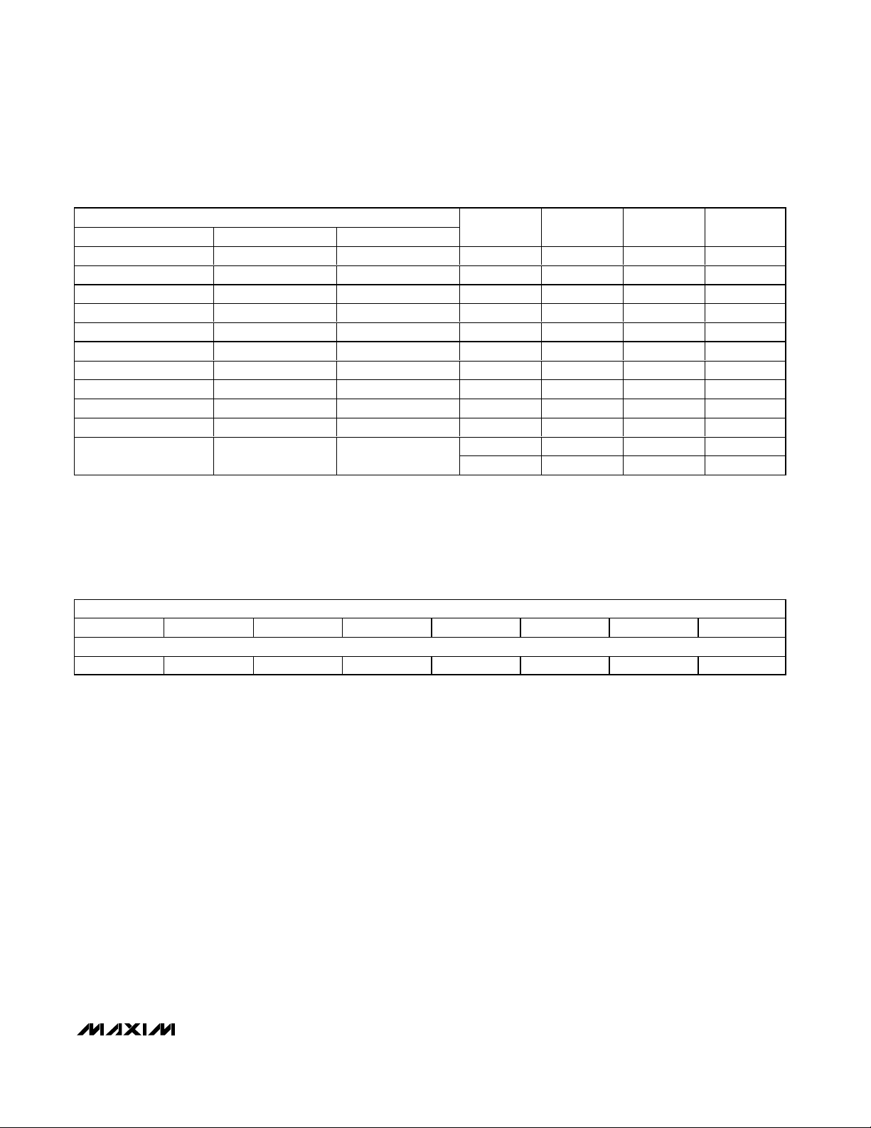
MAX1358/MAX1359/MAX1360
16-Bit Data-Acquisition Systems with ADC, DACs,
UPIOs, RTC, Voltage Monitors, and Temp Sensor
______________________________________________________________________________________ 39
NEGATIVE MUX INPUT
MAX1358 MAX1359 MAX1360
MUXN3 MUXN2 MUXN1 MUXN0
TEMP- TEMP- TEMP- 0 0 0 0
SNO2 SNO2 SNO2 0 0 0 1
OUTA OUTA OUT3 0 0 1 0
SCM2 SCM2 SCM2 0 0 1 1
OUTB OUT2 OUT2 0 1 0 0
SNC2 SNC2 SNC2 0 1 0 1
OUT1 OUT1 OUT1 0 1 1 0
AIN2 AIN2 AIN2 0 1 1 1
REF REF REF 1 0 0 0
AGND AGND AGND 1 0 0 1
101X
Open Open Open
11XX
Table 9. Selecting the Negative MUX Inputs
MSB
ADC15 ADC14 ADC13 ADC12 ADC11 ADC10 ADC9 ADC8
LSB
ADC7 ADC6 ADC5 ADC4 ADC3 ADC2 ADC1 ADC0
DATA Register (Power-On State: 0000 0000 0000 0000)
X = Don’t care.
ADC<15:0> Analog-to-digital conversion data bits.
These 16 bits are the results from the most recently
completed conversion. The data format is unsigned,
binary for unipolar mode, and two’s complement for
bipolar mode.
Page 40

MAX1358/MAX1359/MAX1360
16-Bit Data-Acquisition Systems with ADC, DACs,
UPIOs, RTC, Voltage Monitors, and Temp Sensor
40 ______________________________________________________________________________________
The OFFSET CAL register contains the 24-bit data of
the most recently completed offset calibration.
OFFSET<23:0>: Offset-calibration bits. The data format
is two’s complement and is subtracted from the ADC
output before being written to the DATA register. The
offset calibration allows input offset errors between
V
REF
±50% to be corrected in unipolar or bipolar mode.
The MAX1358/MAX1359/MAX1360 can perform system
offset calibration or self offset calibration. Self-calibration performs a calibration for the entire signal path.
See the ADC Calibration section for more details.
The ADC input voltage range specifications must
always be obeyed and the OFFSET CAL register effectively offsets the ADC digital scale to a “zero” value
determined by the calibration.
MSB
OFFSET23 OFFSET22 OFFSET21 OFFSET20 OFFSET19 OFFSET18 OFFSET17 OFFSET16
OFFSET15 OFFSET14 OFFSET13 OFFSET12 OFFSET11 OFFSET10 OFFSET9 OFFSET8
LSB
OFFSET7 OFFSET6 OFFSET5 OFFSET4 OFFSET3 OFFSET2 OFFSET1 OFFSET0
OFFSET CAL Register (Power-On State: 0000 0000 0000 0000 0000 0000)
MSB
GAIN23 GAIN22 GAIN21 GAIN20 GAIN19 GAIN18 GAIN17 GAIN16
GAIN15 GAIN14 GAIN13 GAIN12 GAIN11 GAIN10 GAIN9 GAIN8
LSB
GAIN7 GAIN6 GAIN5 GAIN4 GAIN3 GAIN2 GAIN1 GAIN0
GAIN CAL Register (Power-On State: 1000 0000 0000 0000 0000 0000)
GAIN<23:0>: Gain-calibration bits. The data format is
unsigned binary with 23 bits to the right of the decimal
point and scales the ADC output before being written to
the DATA register. The gain calibration allows full-scale
errors between -V
REF
/ 2 and +V
REF
/ 2 to be corrected
in unipolar mode, and full-scale errors between (+50%
x V
REF
) and (+200% x V
REF
) in unipolar or bipolar
mode. The MAX1358/MAX1359/MAX1360 can perform
system gain calibration or self gain calibration. Self-calibration performs a calibration for offsets in the ADC and
system calibration performs a calibration for the entire
signal path. See the ADC Calibration section for more
details.
The ADC input voltage range specifications must always
be obeyed and the GAIN CAL register effectively scales
the ADC digital output to a full-scale value determined
by the calibration. The usable gain-calibration range is
limited to less than the full GAIN CAL register digitalscaling range by the internal noise of the ADC.
Page 41

MAX1358/MAX1359/MAX1360
16-Bit Data-Acquisition Systems with ADC, DACs,
UPIOs, RTC, Voltage Monitors, and Temp Sensor
______________________________________________________________________________________ 41
DACA_OP Registers
Writing to the DACA_OP output register updates DACA
on the rising SCLK edge of the LSB data bit. The output
voltage can be calculated as follows:
V
OUTA
= V
REF
x N / 2
10
where
V
REF
is the reference voltage for the DAC.
N is the integer value of DACA<9:0> output register.
The output buffer is in unity gain.
The DACA data is 10 bits long and right justified.
DAE: DACA enable bit. Set DAE = 1 to power up the
DACA and the DACA output buffer in the MAX1358/
MAX1359. This bit is mirrored in the DACB_OP register.
DBE: DACB enable bit. Set DBE = 1 to power up
DACB and the DACB output buffer in the MAX1358.
This bit is mirrored in the DACB_OP register.
OP1E: OP1 power-enable bit. Set OP1E = 1 to power
up OP1 in the MAX1358/MAX1359/MAX1360. This bit is
mirrored in the DACB_OP register.
OP2E: OP2 power-enable bit. Set OP2E = 1 to power
up OP2 in the MAX1359/MAX1360. This bit is mirrored
in the DACB_OP register.
OP3E: OP3 power-enable bit. Set OP3E = 1 to power
up OP3 in the MAX1360. This bit is mirrored in the
DACB_OP register.
DACA<9:0>: DACA data bits.
MSB
DAE DBE OP1E X X X DACA9 DACA8
LSB
DACA7 DACA6 DACA5 DACA4 DACA3 DACA2 DACA1 DACA0
MAX1358 (Power-On State: 000X XX00 0000 0000)
MSB
DAE OP2E OP1E X X X DACA9 DACA8
LSB
DACA7 DACA6 DACA5 DACA4 DACA3 DACA2 DACA1 DACA0
MAX1359 (Power-On State: 000X XX00 0000 0000)
MSB
OP3E OP2E OP1E X X X X X
LSB
XXXXXXXX
MAX1360 (Power-On State: 000X XXXX XXXX XXXX)
Page 42

MAX1358/MAX1359/MAX1360
16-Bit Data-Acquisition Systems with ADC, DACs,
UPIOs, RTC, Voltage Monitors, and Temp Sensor
42 ______________________________________________________________________________________
DACB_OP Registers
Writing to the DACB_OP output register updates DACB
on the rising SCLK edge of the LSB. The output voltage
can be calculated as follows:
V
OUTB
= V
REF
x N / 2
10
where
V
REF
is the reference voltage for the DAC.
N is the integer value of DACB<9:0> output register.
The output buffer is in unity gain.
The DACB data is 10 bits long and right justified.
MSB
DAE DBE OP1E X X X DACB9 DACB8
LSB
DACB7 DACB6 DACB5 DACB4 DACB3 DACB2 DACB1 DACBD
MAX1358 (Power-On State: 000X XX00 0000 0000)
MSB
DAE OP2E OP1E X X X X X
LSB
XXXXXXXX
MAX1359 (Power-On State: 000X XXXX XXXX XXXX)
MSB
OP3E OP2E OP1E X X X X X
LSB
XXXXXXXX
MAX1360 (Power-On State: 000X XXXX XXXX XXXX)
DAE: DACA enable bit. Set DAE = 1 to power up
DACA and the DACA output buffer in the
MAX1358/MAX1359. This bit is mirrored in the
DACA_OP register.
DBE: DACB enable bit. Set DBE = 1 to power up
DACB and the DACB output buffer in the MAX1358.
This bit is mirrored in the DACA_OP register.
OP1E: OP1 power-enable bit. Set OP1E = 1 to power
up OP1 in the MAX1358/MAX1359/MAX1360. This bit is
mirrored in the DACA_OP register.
OP2E: OP2 power-enable bit. Set OP2E = 1 to power
up OP2 in the MAX1359/MAX1360. This bit is mirrored
in the DACA_OP register.
OP3E: OP3 power-enable bit. Set OP3E = 1 to power
up OP3 in the MAX1360. This bit is mirrored in the
DACA_OP register.
DACB<9:0>: DACB data bits.
Page 43

MAX1358/MAX1359/MAX1360
16-Bit Data-Acquisition Systems with ADC, DACs,
UPIOs, RTC, Voltage Monitors, and Temp Sensor
______________________________________________________________________________________ 43
The REF_SDC register contains bits to control the reference voltage and signal-detect comparator.
REFV<1:0>: Reference buffer voltage gain and enable
bits. Enables the output buffer, sets the gain and the
voltage at the REF pin as shown in Table 10. Power-on
state is off to enable an external reference to drive the
REF pin without contention.
AOFF: ADC and DAC/op-amp power-off bit. This bit provides a method for turning off several analog functions
with a single write. Setting AOFF = 1 deasserts the
ADCE in the ADC register and DAE/OP3E, DBE/OP2E,
and OP1E bits in the DACA_OP and DACB_OP registers, powering down these analog blocks. Setting AOFF
= 0 has no effect. The AON bit has priority when both
AON and AOFF bits are asserted.
Most of the analog functions can be disabled with a
single write to the REF_SDC register by using AOFF,
REFV<1:0>, and SDCE.
AON: ADC and DAC/op-amp power-on bit. This bit
provides a method of turning on several analog functions with a single write. Setting AON = 1 asserts the
ADCE bit in the ADC register and DAE/OP3E,
DBE/OP2E, and OP1E bits in the DACA_OP and
DACB_OP registers, powering up these blocks. Setting
AON = 0 has no effect. The AON bit has priority when
both AON and AOFF bits are asserted.
Most of the analog functions can be enabled with a single write to the REF_SDC register using AON,
REFV<1:0>, and SDCE.
SDCE: Signal-detect comparator power-enable bit. Set
SDCE = 1 to power up the signal-detect comparator
and set SDCE = 0 to power down the signal-detect
comparator. The ADCE bit in the ADC register must be
set to 1 to use the signal-detect comparator.
TSEL<2:0>: Threshold-select bits. These bits select the
threshold for the signal-detect comparator as shown in
Table 11.
MSB LSB
REFV1 REFV0 AOFF AON SDCE TSEL2 TSEL1 TSEL0
REF_SDC Register (Power-On State: 0000 0000)
REFERENCE
BUFFER GAIN (V/V)
REF OUTPUT
VOLTAGE (V)
REFV1
REFV0
Disabled
Off (High
00
1.0 1.25 0 1
1.638 2.048 1 0
2.0 2.5 1 1
Table 10. Setting the Reference Output
Voltage
NOMINAL
THRESHOLD (mV)
TSEL2 TSEL1 TSEL0
00XX
50 100
100 1 0 1
150 1 1 0
200 1 1 1
Table 11. Setting the Signal-Detect
Comparator Threshold
X = Don’t care.
Impedance at REF)
Page 44
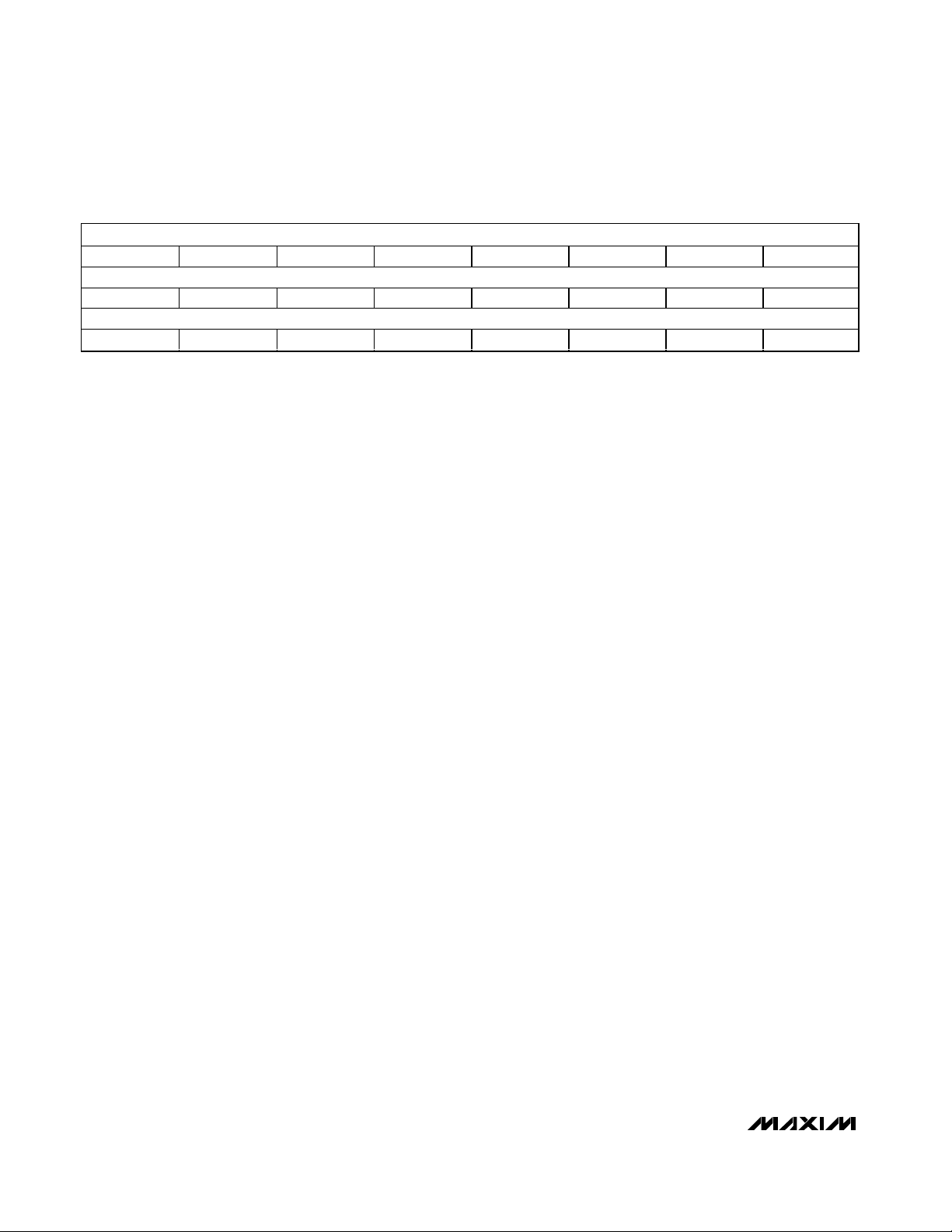
MAX1358/MAX1359/MAX1360
16-Bit Data-Acquisition Systems with ADC, DACs,
UPIOs, RTC, Voltage Monitors, and Temp Sensor
44 ______________________________________________________________________________________
MSB
ASEC19 ASEC18 ASEC17 ASEC16 ASEC15 ASEC14 ASEC13 ASEC12
ASEC11 ASEC10 ASEC9 ASEC8 ASEC7 ASEC6 ASEC5 ASEC4
LSB
ASEC3 ASEC2 ASEC1 ASEC0 X X X X
AL_DAY Register (Power-On State: 0000 0000 0000 0000 0000 XXXX)
The AL_DAY register stores the second information of
the time-of-day alarm.
ASEC<19:0>: Alarm-second bits. These 20 bits store
the time-of-day alarm, which corresponds to the lower
20 bits of the RTC second counter or SEC<19:0>.
Program the time-of-day alarm trigger between 1s to
just over 12 days beyond the current RTC second
counter value in increments of 1s.
Assert the AWE bit in the CLK_CTRL register (see the
CLK_CTRL Register section) to enable writing to the
AL_DAY register. Enabling the time-of-day alarm requires
two writes to the CLK_CTRL register. Write the 20 alarmsecond bits in 3 bytes, MSB first. If CS is raised before
the LSB is written, the alarm write is aborted, and the
existing value remains. When the lower 20 bits in the RTC
second counter match the contents of this register, the
alarm triggers and asserts ALD in the STATUS register. It
also asserts an interrupt on the INT pin unless masked by
the MALD bit in the IMSK register. The part enters normal
mode if an alarm triggers while in sleep mode. The timeof-day alarm is intended to trigger single events.
Therefore, once it triggers, in the CLK_CTRL register, the
ADE bit is automatically cleared, disabling the time-ofday alarm. Implement a recurring alarm with repeated
software writes over the serial interface each time the
time-of-day alarm triggers. The time-of-day alarm can
also be programmed to output at the UPIO pins.
When configured this way the MALD bit does not mask
the UPIO alarm output.
Page 45
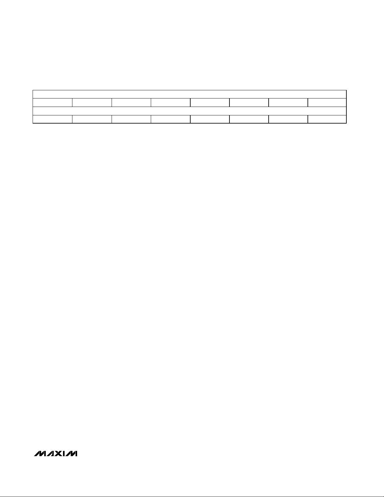
MAX1358/MAX1359/MAX1360
16-Bit Data-Acquisition Systems with ADC, DACs,
UPIOs, RTC, Voltage Monitors, and Temp Sensor
______________________________________________________________________________________ 45
The CLK_CTR register contains the control bits for the
RTC alarms and clocks.
AWE: Alarm write-enable bit. Set AWE = 1 to write data
to the AL_DAY register as well as the ADE bit in this
register. When AWE = 0, all writes are prevented to the
AL_DAY register and the ADE bit in this register. A second write to this register is required to change the value
of the ADE bit. The power-on default state is 0.
ADE: Alarm (time-of-day) enable bit. Set ADE = 1 to
enable the time-of-day alarm and set ADE = 0 to disable the time-of-day alarm. When enabled, the ALD bit
in the STATUS register asserts when the RTC second
counter time matches AL_DAY register. The device
wakes up from sleep to normal mode if not already
awake. The ADE bit can only be written if the AWE = 1
from a previous write. The power-on default state is 0.
RWE: RTC write-enable bit. Set RWE = 1 prior to writing
to the RTC register and the RTCE bit in this register. If
RWE = 0, all writes are prevented to the RTC register
as well as the RTCE bit in this register. The RWE signal
takes effect after the rising edge of the 16th clock;
therefore, a second write to this register is required to
change the value of the RTCE bit. The power-on default
state is 0.
RTCE: Real-time-clock enable bit. Set RTCE = 1 to
enable the RTC, and set RTCE = 0 to disable the RTC.
The RTC has a 32-bit second and an 8-bit subsecond
counter. The power-on default state is 1.
OSCE: 32kHz crystal-oscillator enable bit. Set OSCE =
1 to power up the 32kHz oscillator and set OSCE = 0 to
power down the oscillator. The power-on default state
is 1.
FLLE: Frequency-locked-loop enable bit. Set FLLE = 1
to enable the FLL, and set FLLE = 0 to disable the FLL.
If HFCE = 1 and FLLE = 0, the internal high-frequency
oscillator is enabled but it is not frequency-locked to
the 32kHz clock. When FLLE is asserted, it typically
takes 3.5ms for the high-frequency clock to settle to
within 1% of the 32kHz reference clock frequency.
Switching the FLL on or off with this bit does not cause
high-frequency clock glitching. The power-on default
state is 1.
MSB
AWE ADE X RWE RTCE OSCE FLLE HFCE
LSB
CKSEL2 CKSEL1 CKSEL0 IO32E CK32E CLKE INTP WDE
CLK_CTRL Register (Power-On State: 00X0 1111 0010 1110)
Page 46

MAX1358/MAX1359/MAX1360
16-Bit Data-Acquisition Systems with ADC, DACs,
UPIOs, RTC, Voltage Monitors, and Temp Sensor
46 ______________________________________________________________________________________
HFCE: High-frequency-clock enable bit. Set HFCE = 1
to enable the internal high-frequency clock source, and
set HFCE = 0 to disable the high-frequency clock
source.
If HFCE = 1 and CLKE = 1, the internal high-frequency
oscillator is enabled and is present at CLK. The poweron default state is 1.
CKSEL<2:0>: Clock selection bits. These bits select
the FLL-based output clock frequency at the high-frequency CLK pin as shown in Table 12. The power-on
default state is 001.
IO32E: Input/output 32kHz clock select bit. Set IO32E
= 0 to configure the CLK32K pin as an output and set
IO32E = 1 to configure the CLK32K pin as an input,
regardless of the signal on the 32KIN pin as shown in
Table 13.
External clock frequencies applied to CLK32K are
clock sources to the FLL, charge pump, and the signaldetect comparator. The default power-on state is 0.
CK32E: CLK32K output-buffer enable bit. Set CK32E =
1 to enable the CLK32K output buffer as long as OSCE
= 1 and IO32E = 0, otherwise the CK32E bit will not be
asserted. Set CK32E = 0 to disable the CLK32K output
buffer. The power-on default state is 1.
CLKE: CLK output-buffer enable bit. Set CLKE = 1 to
enable the CLK output buffer. Set CLKE = 0 to disable
the buffer. Disabling the buffer is useful for saving
power in cases where the high-frequency clock is used
internally but is not needed externally. If HFCE = 0, or if
CLKE = 0, CLK remains low. The power-on default
state is 1.
INTP: Interrupt pin polarity bit. Set INTP = 1 to make
INT an active-high output when asserted and set INTP
= 0 to make INT an active-low output when asserted.
The power-on default state is 1.
WDE: Watchdog-enable bit. Set WDE = 1 to enable the
watchdog timer, which asserts RESET low within 500ms
if the WATCHDOG register is not written. Set WDE = 0
to disable the watchdog timer. The power-on default
state is 0.
CLOCK FREQUENCY
(kHz)
CKSEL2
CKSEL1
CKSEL0
4915.2 0 0 0
2457.6 0 0 1
1228.8 0 1 0
614.4 0 1 1
32.768 1 0 0
16.384 1 0 1
8.192 1 1 0
4.096 1 1 1
Table 12. Setting the CLK Frequency
CLK32K
IO32E
RTC, PWM, WDT
CLOCK SOURCE
FLL, C/P, SDC INPUT
SOURCE
ADC CLOCK SOURCE
Output
10XTAL attached XTAL XTAL FLL/HFCLK
Input 0 1 XTAL attached XTAL CLK32K FLL/HFCLK
Table 13. Configuring the CLK32K as an Input or Output
CLK32K
32KIN, 32KOUT
Page 47

MAX1358/MAX1359/MAX1360
16-Bit Data-Acquisition Systems with ADC, DACs,
UPIOs, RTC, Voltage Monitors, and Temp Sensor
______________________________________________________________________________________ 47
The RTC register stores the 40-bit second and subsecond count of the respective time-of-day and system
clocks.
SEC<31:0>: The second bits store the time-of-day
clock settings. It is a 32-bit binary counter with 1s resolution that can keep time for a span of over 136 years.
Firmware in the µC can translate this time count to units
that are meaningful to the system (i.e., translate to calendar time or as an elapsed time from some predefined
time = 0, such as January 1, 2000). The RTC runs continuously as long as RTCE = 1 (see the CLK_CNTL
Register section) and does not stop for reads or writes.
The counter increments when the subsecond counter
overflows. Set RWE = 1 to enable writing to the RTC
register. After writing to RWE, perform another write
and set RTCE = 1 to enable the RTC. A 40-bit burst
write operation, starting with SEC31 and finishing with
SUB0 is required to set the RTC second and subsecond bits. If CS is brought high before the 40th rising
SCLK edge, the write is aborted and the RTC contents
are unchanged. The RTC register is loaded on the rising SCLK edge of the 40th bit (SUB0). A 40-bit burst
read operation, starting with SEC31 and finishing with
SUB0, is required to retrieve the current RTC second
and subsecond counts. The read command can be
aborted prior to receiving the 40th bit (SUB0) by raising
CS and any RTC data read to that point is valid. When
the read command is received, a snapshot of a valid
RTC second count is latched to avoid reading an erroneous, transitioning RTC value. Due to the asynchronous nature of RTC reads, it is possible to have a
maximum 1s error between the actual and reported
times from the time-of-day clock. To prevent the data
from changing during a read operation, complete reads
of the RTC register in less than 1ms. The power-on
default state is 0000 0000 hex.
SUB<7:0>: The subsecond bits store the system clock.
This 8-bit binary counter has 3.9ms resolution (1/256Hz)
and a span of 1s. The subsecond counter increments in
single counts from 00 hex to FF hex before rolling over
again to 00 hex, at which time, the RTC second counter
(SEC<31:0>) increments. The RTC runs continuously
(as long as RTCE = 1) and does not stop for reads or
writes. A 256Hz clock, derived from the 32kHz crystal,
increments this counter. Set the RWE = 1 bit to enable
writing to the RTC register. After writing to RWE, perform
another write, setting RTCE = 1, to enable the RTC. A
40-bit burst write operation, starting with SEC31 and finishing with SUB0, is required to set the RTC second and
subsecond bits. If CS is brought high before the 40th
rising SCLK edge, the write is aborted and the RTC contents are unchanged. The RTC register is loaded on the
rising SCLK edge of the 40th bit (SUB0). A 40-bit burst
read operation, starting with SEC31 and finishing with
SUB0, is required to retrieve the current RTC second
and subsecond counts. The read command can be
aborted prior to receiving the 40th bit (SUB0) by raising
CS and any RTC data read to that point is valid. When
the read command is received, a snapshot of a valid
RTC second count is latched to avoid reading an erroneous, transitioning RTC value. Due to the asynchronous nature of RTC reads, it is possible to have a
maximum 1s error between the actual and reported
times from the time-of-day clock. To prevent the data
from changing during a read operation, complete reads
of the RTC registers occur in less than 1ms. The poweron default state is 00 hex.
MSB
SEC31 SEC30 SEC29 SEC28 SEC27 SEC26 SEC25 SEC24
SEC23 SEC22 SEC21 SEC20 SEC19 SEC18 SEC17 SEC16
SEC15 SEC14 SEC13 SEC12 SEC11 SEC10 SEC9 SEC8
SEC7 SEC6 SEC5 SEC4 SEC3 SEC2 SEC1 SEC0
LSB
SUB7 SUB6 SUB5 SUB4 SUB3 SUB2 SUB1 SUB0
RTC Register (Power-On State: 0000 0000 0000 0000 0000 0000 0000 0000 0000 0000)
Page 48

MAX1358/MAX1359/MAX1360
16-Bit Data-Acquisition Systems with ADC, DACs,
UPIOs, RTC, Voltage Monitors, and Temp Sensor
48 ______________________________________________________________________________________
The PWM_CTRL register contains control bits for the 8bit PWM.
PWME: PWM-enable bit. Set PWME = 1 to enable the
internal PWM and set PWME = 0 to disable the internal
PWM. Enable the high frequency clock before enabling
the PWM when using input clock frequencies above
32.768kHz. The power-on default state is 0.
FSEL<2:0>: Frequency selection bits. Selects the PWM
input clock frequency as shown in Table 14. The
power-on default is 000.
SWAH: SWA-switch PWM-high control bit. Set SWAH =
1 to enable the PWM output to directly control the SWA
switch. When SWAH = SWAL, the PWM output is disabled from controlling the SWA switch. When SWAH =
1, a PWM high output closes the SWA switch and a
PWM low output opens the SWA switch. The PWM high
output refers to the beginning of the period when the
output is logic-high. See Table 17 for more details. The
power-on default is 0.
SWAL: SWA-switch PWM-low control bit. Set SWAL = 1
to enable the inverted PWM output to directly control
the SWA switch. When SWAH = SWAL, the PWM output
is disabled from controlling the SWA switch. When
SWAL = 1, a PWM low output closes the SWA switch
and a PWM high output opens the SWA switch. The
PWM low output refers to the end of the period when
the output is logic-low. See Table 17 for more details.
The power-on default is 0.
SWBH: SWB-switch PWM-high control bit. Set SWBH =
1 to enable the PWM output to directly control the SWB
switch. When SWBH = SWBL, the PWM output is disabled from controlling the SWB switch. When SWBH =
1, a PWM high output closes the SWB switch and a
PWM low output opens the SWB switch. The PWM high
output refers to the beginning of the period when the
output is logic-high. See Table 18 for more details. The
power-on default is 0.
SWBL: SWB-switch PWM-low control bit. Set SWBL = 1
to enable the inverted PWM output to directly control
the SWB switch. When SWBH = SWBL the PWM output
is disabled from controlling the SWB switch. When
SWBL = 1, a PWM low output closes the SWB switch
and a PWM high output opens the SWB switch. The
PWM low output refers to the end of the period when
the output is logic-low. See Table 18 for more details.
The power-on default is 0.
SPD1: SPDT1-switch PWM drive control bit. Set SPD1
= 1 to enable the PWM output to directly control the
SPDT1 switch and set SPD1 = 0 to disable the PWM
output controlling the SPDT1 switch. The SPDT1<1:0>
bits, the UPIO pins (if programmed), and the PWM output (if enabled), determine the SPDT1-switch state. See
Table 19 for more details. The power-on default is 0.
SPD2: SPDT2-switch PWM drive control bit. Set SPD2
= 1 to enable the PWM output to directly control the
SPDT2 switch and set SPD2 = 0 to disable the PWM
output controlling the SPDT2 switch. The SPDT2<1:0>
bits, the UPIO pins (if programmed), and the PWM output (if enabled), determine the SPDT2-switch state. See
Table 20 for more details. The power-on default is 0.
MSB
PWME FSEL2 FSEL1 FSEL0 SWAH SWAL SWBH SWBL
LSB
SPD1 SPD2 X X X X X X
PWM_CTRL Register (Power-On State: 0000 0000 00XX XXXX)
PWM INPUT FREQUENCY*
(kHz)
FSEL2
FSEL1
FSEL0
4915.2** 0 0 0
2457.6** 0 0 1
1228.8** 0 1 0
32.768 0 1 1
8.192 1 0 0
1.024 1 0 1
0.256 1 1 0
0.032 1 1 1
Table 14. Setting the PWM Frequency
*The lower PWM frequencies are useful for power-supply duty
cycling to conserve battery life and enable a single battery cellpowered system. The higher frequencies allow reasonably small,
external components for RC filtering when used as a DAC for bias
adjustments.
**When the part is in sleep mode, the HFCK is shut down. In this
case, PWM frequencies above 32kHz are not available (see
SPWME in the SLEEP_CFG Register section).
Page 49

MAX1358/MAX1359/MAX1360
16-Bit Data-Acquisition Systems with ADC, DACs,
UPIOs, RTC, Voltage Monitors, and Temp Sensor
______________________________________________________________________________________ 49
MSB
PWMTH7 PWMTH6 PWMTH5 PWMTH4 PWMTH3 PWMTH2 PWMTH1 PWMTH0
LSB
PWMTP7 PWMTP6 PWMTP5 PWMTP4 PWMTP3 PWMTP2 PWMTP1 PWMTP0
PWM_THTP Register (Power-On State: 0000 0000 0000 0000)
The PWM_THTP register contains the bits that set the
PWM on-time and period.
PWMTH<7:0>: PWM time high bits. These bits define
the PWM on (or high) time and when combined with the
PWMTP<7:0> bits, they determine the duty cycle and
period. The on-time duty cycle is defined as:
(PWMTH<7:0> + 1) / (PWMTP<7:0> + 1)
To get 50% duty cycle, set PWMTH<7:0> to 127 decimal and PWMTP<7:0> to 255 decimal. A 100% duty
cycle (i.e., always on) is possible with a value of
PWMTH<7:0> ≥ PWMTP<7:0> > 0. A 0% duty cycle is
possible by setting PWMTH<7:0> = 0 or PWME = 0 in
the PWM_CTRL register. If the PWM is selected to drive
the UPIO_ pin(s), the ALH_ bit(s) (UPIO_CTRL register)
determine the on-time polarity at the beginning of the
PWM cycle. If ALH_= 1, the on-time at the start of the
PWM period causes a logic-high level (DV
DD
or
CPOUT) at the UPIO_ pin and when ALH_= 0, it causes
a logic-low level (DGND) during the on-time. When the
PWM output drives the SWA/B switches, the SWA(B)H
or SWA(B)L bits in the PWM_CTRL register, determine
which PWM phase closes these switches. The SPDT1
and SPDT2 switches do not have PWM polarity inversion bits (see the SPDT1<1:0> and SPDT2<1:0> bit
descriptions in the SW_CTRL Register section) but their
effective polarity is set by how the switches are connected externally. The power-on default is 00 hex.
PWMTP<7:0>: PWM time period bits. These bits control the PWM output period defined. The PWM output
period is defined as:
(PWMTP<7:0> + 1) / (PWM input frequency)
Set the PWM input frequency by selecting the
FSEL<2:0> bits as described in Table 14. The poweron default is 00 hex.
WATCHDOG Register (Power-On State: N/A)
Writing to the WATCHDOG register address sets the
watchdog timer to 0ms. If the watchdog is enabled
(WDE = 1) and the WATCHDOG register is not written
to before the 750ms expiration, RESET asserts low for
250ms and the watchdog timer restarts at 0ms when
the watchdog timer is enabled. There are no data bits
for this register and the watchdog timer is reset on the
rising edge of SCLK during the ADR0 bit in the
WATCHDOG register address control byte. Figure 19
shows an example of watchdog timing.
NORM_MD Register (Power-On State: N/A)
Exit sleep mode and enter normal mode by writing to
the NORM_MD register. The specific normal-mode
state of all circuit blocks is set by the user, who must
configure the individual power-enable bits before entering sleep mode (Table 15). There are no data bits for
this register and normal mode begins on the rising
edge of SCLK during the ADR0 bit in the NORM_MD
register address control byte.
SLEEP Register (Power-On State: N/A)
Enter sleep mode by writing to the SLEEP register. This
low-power state overrides most of the normal powercontrol bits. Table 15 shows which functions are off,
which functions are unaffected (ADE, RTCE, LSDE, and
HYSE), and which functions are controlled by special
sleep-mode bits (SOSCE, SCK32E, and SPWME) while
in sleep mode. There are no data bits for this register
and sleep mode begins on the rising edge of SCLK
during the ADR0 bit in the SLEEP register address control byte.
Page 50

MAX1358/MAX1359/MAX1360
16-Bit Data-Acquisition Systems with ADC, DACs,
UPIOs, RTC, Voltage Monitors, and Temp Sensor
50 ______________________________________________________________________________________
REGISTER
NAME
CIRCUIT BLOCK
DESCRIPTION
POR DEFAULT NORMAL MODE SLEEP
ADC ADC ADCE = 0 ADCE OFF
DACA/OP3 DAE/OP3E = 0 DAE/OP3E OFF
DACB/OP2 DBE/OP2E = 0 DBE/OP2E OFF
DACA_OP,
DACB_OP
OP1 OP1E = 0 OP1E OFF
Reference Buffer Gain and
Enable
REFV<1:0> = 00 REFV<1:0> OFF
REF_SDC
Signal-Detect Comparator SDCE = 0 SDCE OFF
Time-of-Day Alarm Enable ADE = 0 ADE ADE
RTC RTCE = 1 RTCE RTCE
CK32 Xtal Oscillator OSCE = 1 OSCE SOSCE
CK32 Output Buffer CK32E = 1 CK32E SCK32E
High-Frequency Clock HFCE = 1 HFCE OFF
High-Frequency Clock Output
Buffer
CLKE = 1 CLKE OFF
FLL Enable FLLE = 1 FLLE OFF
CLK_CTRL
Watchdog Timer WDE = 0 WDE OFF
PWM_CTRL PWM PWME = 0 PWME SPWME
Linear Regulator LDOE = 0 LDOE OFF
Charge-Pump Doubler CPE = 0 CPE OFF
CPOUT Voltage Monitor CPDE = 0 CPDE OFF
1.8V DVDD Monitor LSDE = 1 LSDE LSDE
PS_VMONS
1.8V Monitor Hysteresis HYSE = 0 HYSE HYSE
TEMP_CTRL Temperature Sense Source IMUX<1:0> = 00 IMUX<1:0> OFF
UPIO_ Function UP_MD<3:0> = 0 hex UP_MD<3:0> UP_MD<3:0>
UPIO_ Pullup PUP_ = 1 PUP_ PUP_
UPIO_ Supply Voltage SV_ = 0 SV_ SV_
UPIO_CTRL
UPIO_ Assertion Level ALH_ = 0 ALH_ ALH_
Table 15. Normal-Mode and Sleep-Register Summary
Page 51

MAX1358/MAX1359/MAX1360
16-Bit Data-Acquisition Systems with ADC, DACs,
UPIOs, RTC, Voltage Monitors, and Temp Sensor
______________________________________________________________________________________ 51
The SLEEP_CFG register allows users to program specific behavior for the 32kHz oscillator, buffer, and PWM
in sleep mode. It also contains a sleep-control bit (SLP)
to enable sleep mode.
SLP (ADR0): Sleep bit. The SLP bit is the LSB in the
SLEEP_CFG address control byte. Set SLP = 1 to
assert the SHDN bit and enter sleep mode. Writing the
register with SLP = 0 or reading with SLP = 0 or SLP =
1 has no effect on the SHDN bit.
SOSCE: Sleep mode 32kHz crystal oscillator enable
bit. SOSCE = 1 enables the 32kHz oscillator in sleep
mode and SOSCE = 0 disables it in sleep mode,
regardless of the state of the OSCE bit. The power-on
default is 1.
SCK32E: Sleep-mode CK32K-pin output-buffer enable
bit. SCK32E = 1 enables the 32kHz output buffer in
sleep mode and SCK32E = 0 disables it in sleep mode,
regardless of the state of the CK32E bit. The power-on
default is 1.
SPWME: Sleep mode PWM enable bit. SPWME = 1
enables the internal PWM in sleep mode and SPWME =
0 disables it in sleep mode, regardless of the state of the
PWME bit.
Input frequencies are limited to 32.768kHz or lower
since the high-frequency clock is disabled in sleep
mode. SOSCE must be asserted to have 32kHz available as an input to the PWM. The power-on default is 0.
SHDN: Shutdown bit. This bit is read only. SHDN is
asserted by writing to the SLEEP register address or by
writing to the SLEEP_CFG register with SLP = 1. When
SHDN is asserted, the device is in sleep mode even if
the SLEEP or SLEEP function on the UPIO is deasserted. The SHDN bit is deasserted by writing to the
NORM_MD register or by other defined events. Events
that cause SHDN to be deasserted are a day alarm or
an edge on the UPIO wake-up pin causing wake-up to
be asserted. The power-on default is 0.
MSB LSB
SLP (ADR0)
SOSCE SCK32E SPWME SHDN X X X X
SLEEP_CFG Register (Power-On State: 1100 XXXX)
4Hz CLOCK
2-BIT COUNTER
X
WDE = 1
012 3
RESET
WATCHDOG
ADDRESS
01 2
WATCHDOG
ADDRESS
WATCHDOG
ADDRESS
01 0120
750ms
250ms
SPI WRITES
D
Q
Q
R
CK
DQ
Q
R
CK
DIVIDE-
BY-8192
32K
WDE
POR
WDW
WATCHDOG TIMER
4Hz
RESET
Figure 19. Watchdog Timer Architecture
Page 52

MAX1358/MAX1359/MAX1360
16-Bit Data-Acquisition Systems with ADC, DACs,
UPIOs, RTC, Voltage Monitors, and Temp Sensor
52 ______________________________________________________________________________________
MSB LSB
UP4MD3 UP4MD2 UP4MD1 UP4MD0 PUP4 SV4 ALH4 LL4
UPIO4_CTRL Register (Power-On State: 0000 1000)
UPIO4_CTRL register. This register configures the
UPIO4 pin functionality.
UP4MD<3:0>: UPIO4-mode selection bits. These bits
configure the mode for the UPIO4 pin. See Table 16 for
a detailed description. The power-on default is 0 hex.
PUP4: Pullup UPIO4 control bit. Set PUP4 = 1 to enable
a weak pullup resistor on the UPIO4 pin and set PUP4 =
0 to disable it. The pullup resistor is connected to either
DVDDor CPOUT as programmed by the SV4 bit. The
pullup is enabled only when UPIO4 is configured as an
input. Open-drain behavior can be simulated at UPIO4
by setting the mode to GPO with LL4 = 0 and by changing the mode to GPI with PUP4 = 0, allowing external
high pullup. The power-on default is 1.
SV4: Supply-voltage UPIO4 selection bit. Set SV4 = 0
to select DVDDas the supply voltage for the UPIO4 pin
and set SV4 = 1 to select CPOUT as the supply voltage. The selected supply voltage applies to all modes
for the UPIO4 pin. The power-on default is 0.
ALH4: Active logic-level assertion high UPIO4 bit. Set
ALH4 = 0 to define the input or output assertion level
for UPIO4 as low except when in GPI and GPO modes.
Set ALH4 = 1 to define the input or output assertion
level as high. For example, asserting ALH4 defines the
UPIO4 output signal as ALARM, while deasserting
ALH4 defines it as ALARM. Similarly, asserting ALH4
defines the UPIO4 input signal as WU, while deasserting ALH4 defines it as WU. The power-on default is 0.
LL4: Logic-level UPIO4 bit. When UPIO4 is configured
as GPO, LL4 = 0 sets the output to a logic-low and LL4
= 1 sets the output to a logic-high. A read of LL4
returns the voltage level at the UPIO4 pin at the time of
the read regardless of how it is programmed. The
power-on default is 0.
MSB LSB
UP3MD3 UP3MD2 UP3MD1 UP3MD0 PUP3 SV3 ALH3 LL3
UPIO3_CTRL Register (Power-On State: 0000 1000)
UPIO3_CTRL register. This register configures the
UPIO3 pin functionality.
UP3MD<3:0>: UPIO3-mode selection bits. These bits
configure the mode for the UPIO3 pin. See Table 16 for
a detailed description. The power-on default is 0 hex.
PUP3: Pullup UPIO3 control bit. Set PUP3 = 1 to enable
a weak pullup resistor on the UPIO3 pin and set PUP3
= 0 to disable it. The pullup resistor is connected to
either DV
DD
or CPOUT as programmed by the SV3 bit.
The pullup is enabled only when UPIO3 is configured
as an input. Open-drain behavior can be simulated at
UPIO3 by setting the mode to GPO with LL3 = 0 and by
changing the mode to GPI with PUP3 = 0, allowing
external high pullup. The power-on default is 1.
SV3: Supply-voltage UPIO3 selection bit. Set SV3 = 0
to select DVDDas the supply voltage for the UPIO3 pin
and set SV3 = 1 to select CPOUT as the supply voltage. The selected supply voltage applies to all modes
for the UPIO3 pin. The power-on default is 0.
ALH3: Active logic-level assertion high UPIO3 bit. Set
ALH3 = 0 to define the input or output assertion level
for UPIO3 as low except when in GPI and GPO modes
and set ALH3 = 1 to define the input or output assertion
level as high. For example, asserting ALH3 defines the
UPIO3 output signal as ALARM, while deasserting
ALH3 defines it as ALARM. Similarly, asserting ALH3
defines the UPIO3 input signal as WU, while deasserting ALH3 defines it as WU. The power-on default is 0.
LL3: Logic-level UPIO3 bit. When UPIO3 is configured
as GPO, LL3 = 0 sets the output to a logic-low and LL3
= 1 sets the output to a logic-high. A read of LL3
returns the voltage level at the UPIO3 pin at the time of
the read regardless of how it is programmed. The
power-on default is 0.
Page 53

MAX1358/MAX1359/MAX1360
16-Bit Data-Acquisition Systems with ADC, DACs,
UPIOs, RTC, Voltage Monitors, and Temp Sensor
______________________________________________________________________________________ 53
UPIO1_CTRL register. This register configures the
UPIO1 pin functionality.
UP1MD<3:0>: UPIO1-mode selection bits. These bits
configure the mode for the UPIO1 pin. See Table 16 for
a detailed description. The power-on default is 0 hex.
PUP1: Pullup UPIO1 control bit. Set PUP1 = 1 to
enable a weak pullup resistor on the UPIO1 pin and set
PUP1 = 0 to disable it. The pullup resistor is connected
to either DVDDor CPOUT as programmed by the SV1
bit. The pullup is enabled only when UPIO1 is configured as an input. Open-drain behavior can be simulated
at UPIO1 by setting the mode to GPO with LL1 = 0 and
by changing the mode to GPI with PUP1 = 0, allowing
external high pullup. The power-on default is 1.
SV1: Supply-voltage UPIO1 selection bit. Set SV1 = 0
to select DVDDas the supply voltage for the UPIO1 pin
and set SV1 = 1 to select CPOUT as the supply voltage. The selected supply voltage applies to all modes
for the UPIO1 pin. The power-on default is 0.
ALH1: Active logic-level assertion high UPIO1 bit. Set
ALH1 = 0 to define the input or output assertion level
for UPIO1 as low except when in GPI and GPO modes
and set ALH1 = 1 to define the input or output assertion
level as high. For example, asserting ALH1 defines the
UPIO1 output signal as ALARM, while deasserting
ALH1 defines it as ALARM. Similarly, asserting ALH1
defines the UPIO1 input signal as WU, while deasserting ALH1 defines it as WU. The power-on default is 0.
LL1: Logic-level UPIO1 bit. When UPIO1 is configured
as GPO, LL1 = 0 sets the output to a logic-low and LL1
= 1 sets the output to a logic-high. A read of LL1
returns the voltage level at the UPIO1 pin at the time of
the read regardless of how it is programmed. The
power-on default is 0.
MSB LSB
UP2MD3 UP2MD2 UP2MD1 UP2MD0 PUP2 SV2 ALH2 LL2
UPIO2_CTRL Register (Power-On State: 0000 1000)
UPIO2_CTRL register. This register configures the
UPIO2 pin functionality.
UP2MD<3:0>: UPIO2-mode selection bits. These bits
configure the mode for the UPIO2 pin. See Table 16 for
a detailed description. The power-on default is 0 hex.
PUP2: Pullup UPIO2 control bit. Set PUP2 = 1 to
enable a weak pullup resistor on the UPIO2 pin and set
PUP2 = 0 to disable it. The pullup resistor is connected
to either DV
DD
or CPOUT as programmed by the SV2
bit. The pullup is enabled only when UPIO2 is configured as an input. Open-drain behavior can be simulated
at UPIO2 by setting the mode to GPO with LL2 = 0 and
by changing the mode to GPI with PUP2 = 0, allowing
external high pullup. The power-on default is 1.
SV2: Supply-voltage UPIO2 selection bit. Set SV2 = 0
to select DVDDas the supply voltage for the UPIO2 pin
and set SV2 = 1 to select CPOUT as the supply voltage. The selected supply voltage applies to all modes
for the UPIO2 pin. The power-on default is 0.
ALH2: Active logic-level assertion high UPIO2 bit. Set
ALH2 = 0 to define the input or output assertion level
for UPIO2 as low except when in GPI and GPO modes
and set ALH2 = 1 to define the input or output assertion
level as high. For example, asserting ALH2 defines the
UPIO2 output signal as ALARM, while deasserting
ALH2 defines it as ALARM. Similarly, asserting ALH2
defines the UPIO2 input signal as WU, while deasserting ALH2 defines it as WU. The power-on default is 0.
LL2: Logic-level UPIO2 bit. When UPIO2 is configured
as GPO, LL2 = 0 sets the output to a logic-low and LL2
= 1 sets the output to a logic-high. A read of LL2
returns the voltage level at the UPIO2 pin at the time of
the read regardless of how it is programmed. The
power-on default is 0.
MSB LSB
UP1MD3 UP1MD2 UP1MD1 UP1MD0 PUP1 SV1 ALH1 LL1
UPIO1_CTRL Register (Power-On State: 0000 1000)
Page 54

MAX1358/MAX1359/MAX1360
16-Bit Data-Acquisition Systems with ADC, DACs,
UPIOs, RTC, Voltage Monitors, and Temp Sensor
54 ______________________________________________________________________________________
MODE
UP4MD<3:0>, UP3MD<3:0>,
UP2MD<3:0>, UP1MD<3:0>
DESCRIPTION
0000 GPI GPI GPI
General-purpose digital input. Active edges detected
by UPR_ or UPF_ status register bits. ALH_ has no
effect with this setting.
0001 GPO GPO GPO
General-purpose digital output. Logic level set by LL_
bit. ALH_ has no effect with this setting.
0010
X
Digital input. DAC A buffer switch control. See the SWA
bit description in the SW_CTRL Register section.
0011
XX
Digital input. DAC B buffer switch control. See the SWB
bit description in the SW_CTRL Register section.
0100
SPDT1 or
SPDT1
SPDT1 or
SPDT1
SPDT1 or
SPDT1
D i g i tal i np ut. S P D T1 sw i tch contr ol . S ee the S P D T1< 1:0>
b i t d escr i p ti on i n the S W _C TRL Reg i ster secti on.
0101
SPDT2 or
SPDT2
SPDT2 or
SPDT2
SPDT2 or
SPDT2
D i g i tal i np ut. S P D T2 sw i tch contr ol . S ee the S P D T2< 1:0>
b i t d escr i p ti on i n the S W _C TRL Reg i ster secti on.
0110
SLEEP or
SLEEP
SLEEP or
SLEEP
SLEEP or
SLEEP
Sleep-mode digital input. Overrides power-control
register and puts the part into sleep mode when
asserted. When deasserted, power mode is determined
by the SHDN bit.
0111
Wake-up digital input. Asserted edge clears SHDN bit.
1000
1001
1010
Reserved
Reserved. Do not use these settings.
1011
PWM or
PWM
PWM or
PWM
PWM or
PWM
PWM digital output. Signal defined by the PWM_CTRL
register. PWM on (or high or “1”); assertion level defined
by the ALH_ bit. When PWM is disabled (PWME = 0),
the UPIO pin idles high (DV
DD
or CPOUT) if ALH = 1,
and low (DGND) if ALH = 0.
1100
SHDN or
SHDN
SHDN or
SHDN
SHDN or
SHDN
Power-supply shutdown digital output. Equivalent to
SHDN bit. Power-on default of GPI with pullup ensures
initial power-supply turn-on when UPIO is connected to
a power supply with a SHDN input.
1101
AL_DAY or
AL_DAY
AL_DAY or
AL_DAY
AL_DAY or
AL_DAY
RTC alarm digital output. Asserts for time-of-day alarm
events; equivalent to ALD in STATUS register.
1110
Reserved
Reserved. Do not use these settings.
1111
DRDY or
DRDY
DRDY or
DRDY
DRDY or
DRDY
ADC data-ready digital output. Asserts when analog-todigital conversion or calibration completes. Not masked
by MADD bit.
Table 16. UPIO Mode Configuration
Note: When multiple UPIO inputs are configured for the same input function, the inputs are OR’ed together.
MAX1358 MAX1359 MAX1360
SWA or SWA SWA or SWA
SWB or SWB
WU or WU WU or WU WU or WU
Reserved
Reserved
Reserved
Reserved
Page 55
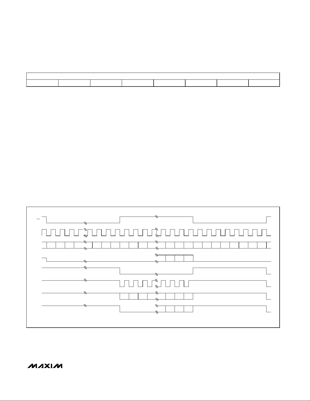
MAX1358/MAX1359/MAX1360
16-Bit Data-Acquisition Systems with ADC, DACs,
UPIOs, RTC, Voltage Monitors, and Temp Sensor
______________________________________________________________________________________ 55
UPIO SPI pass-through control register. These bits map
the serial interface signals to the UPIO pins, allowing
the DAS (MAX1358/MAX1359/MAX1360) to drive other
devices at CPOUT or DVDDvoltage levels, depending
on the SV_ bit setting found in the UPIO_CTRL register.
Individual bits are provided to set only the desired
UPIO inputs to the SPI pass-through mode. This mode
becomes active when CS is driven high to complete the
write to this register, and remains active as long as CS
stays high (i.e., multiple pass-through writes are possible). The SPI pass-through mode is deactivated immediately when CS is pulled low for the next DAS
(MAX1358/MAX1359/MAX1360) write.
The UPIO_ state (both before and after the SPI passthrough mode) is set by the UP_MD<3:0> and LL_ bits.
When a UPIO is configured for SPI pass-through mode
and the CS is high, UPR_, UPF_, and LL_ continue to
detect UPIO_ edges, which can still generate interrupts.
See Figure 20 for an SPI pass-through timing diagram.
UP4S: UPIO4 SPI pass-through-mode enable bit. A
logic 1 maps the inverted CS signal to the UPIO4 pin.
Therefore, UPIO4 is low (near DGND) when SPI passthrough mode is active, and is high (near DV
DD
or
CPOUT) when the mode is inactive. A logic 0 disables
the UPIO4 SPI pass-through mode. The power-on
default is 0.
UP3S: UPIO3 SPI pass-through-mode enable bit. A
logic 1 maps the SCLK signal to UPIO3 (directly with no
inversion), while a logic 0 disables the UPIO3 SPI passthrough mode. The power-on default is 0.
UP2S: UPIO2 SPI pass-through-mode enable bit. A
logic 1 maps the DIN signal to UPIO2 (directly with no
inversion), while a logic 0 disables the UPIO2 SPI passthrough mode. The power-on default is 0.
UP1S: UPIO1 SPI pass-through-mode enable bit. A
logic 1 maps the UPIO1 input signal to DOUT (directly
with no inversion), while a logic 0 disables the UPIO1
SPI pass-through mode. The power-on default is 0.
MSB LSB
UP4S UP3S UP2S UP1S X X X X
UPIO_SPI Register (Power-On State: 0000 XXXX)
CS
WRITE TO DAS TO ENABLE SPI MODE
WRITE THROUGH DAS TO UPIO DEVICE
NORMAL WRITE TO DAS
SCLK
DIN
D
NDN-1DN-2DN-3D3D2D1D0ENEN-1EN-2EN-3
X X X X
E
NEN-1EN-2EN-3
X X X X
D
7D6D5D4D3D2D1D0
DOUT
E
3E2E1E0
E3E2E1E
0
UPIO4
SET BY UPIO4_CTRL REGISTER
SET BY UPIO4_CTRL REGISTER
UPIO3
SET BY UPIO3_CTRL REGISTER
SET BY UPIO3_CTRL REGISTER
UPIO2
SET BY UPIO2_CTRL REGISTER
SET BY UPIO2_CTRL REGISTER
UPIO1
SET BY UPIO1_CTRL REGISTER
SET BY UPIO1_CTRL REGISTER
Figure 20. SPI Pass-Through Timing Diagram
Page 56

MAX1358/MAX1359/MAX1360
16-Bit Data-Acquisition Systems with ADC, DACs,
UPIOs, RTC, Voltage Monitors, and Temp Sensor
56 ______________________________________________________________________________________
The switch-control register controls the two SPDT
switches (SPDT1 and SPDT2) and the two DACA and
DACB output buffer SPST switches (SWA and SWB).
Control these switches by the serial bits in this register,
by any of the UPIO pins that are enabled for that function, or by the PWM.
SWA: (MAX1358/MAX1359) DACA output buffer SPSTswitch A control bit. The SWA bit, the UPIO inputs (if
configured), and the PWM (if configured) control the
state of the SWA switch as shown in Table 17. The
UPIO_ states of 0 and 1 in the table below correspond
to respective deasserted and asserted logic states as
defined by the ALH_ bit of the UPIO_CTRL register. If a
UPIO is not configured for this mode, its value applied
to the table below is 0. The PWM states of 0 and 1 in the
table below correspond to the respective PWM off (or
low) and on (or high) states defined by the SWAH and
SWAL bits (see the PWM_CTRL Register section). If the
PWM is not configured for this mode, its value applied
to the table below is 0. The power-on default is 0.
SWB: (MAX1358 only) DACB output buffer SPST-switch
B control bit. The SWB bit, the UPIO inputs (if configured), and the PWM (if configured) control the state of
the SWB switch as shown in Table 18. The UPIO_ states
of 0 and 1 in the table correspond to respective
deasserted and asserted logic states as defined by the
ALH_ bit (see the UPIO_CTRL Register section). If a
UPIO is not configured for this mode, its value applied
to the table is 0. The PWM states of 0 and 1 in the table
correspond to the respective PWM off (or low) and on
(or high) states defined by the SWBH and SWBL bits
(see the PWM_CTRL Register section). If the PWM is
not configured for this mode, its value applied to the
table is 0. The power-on default is 0.
SPDT1<1:0>: Single-pole double-throw switch 1 control bits. The SPDT1<1:0> bits, the UPIO pins (if configured), and the PWM (if configured) control the state of
the switch as shown in Table 19. The UPIO_ states of 0
and 1 in the table below correspond to respective
deasserted and asserted logic states as defined by the
ALH_ bit of the UPIO_CTRL register. If a UPIO is not
configured for this mode, its value applied to Table 19
is 0. The PWM states of 0 and 1 in Table 19 below correspond to the respective PWM off (low) and on (high)
states defined by the SPD1 bit in the PWM_CTRL register. If the PWM is not configured for this mode, its value
applied to Table 19 is 0. The power-on default is 00.
MSB LSB
SWA SWB SPDT11 SPDT10 SPDT21 SPDT20 X X
SW_CTRL Register (Power-On State: 0000 00XX)
SWA BIT*
UPIO_*
PWM*
SWA SWITCH STATE
000Switch open
XX1Switch closed
X1XSwitch closed
1XXSwitch closed
Table 17. SWA States
X = Don’t care.
*Switch SWA control is effectively an OR of the SWA bit, UPIO
pins, and PWM.
SWB BIT*
UPIO_*
PWM*
SWB SWITCH STATE
000Switch open
XX1Switch closed
X1XSwitch closed
1XXSwitch closed
Table 18. SWB States (MAX1358 Only)
X = Don’t care.
*Switch SWB control is effectively an OR of the SWB bit, UPIO
pins, and PWM.
SPDT1<1:0>
UPIO_*
PWM*
SPDT1 SWITCH STATE
00 00SNO1 open, SNC1 open
0X X 1
SNO1 closed, SNC1 closed
0X 1 X
SNO1 closed, SNC1 closed
01 X X
SNO1 closed, SNC1 closed
10 00SNC1 closed, SNO1 open
1X X1SNC1 open, SNO1 closed
1X 1XSNC1 open, SNO1 closed
11 XXSNC1 open, SNO1 closed
Table 19. SPDT Switch 1 States
X = Don’t care.
*Switch SPDT1 control is effectively an OR of the SPDT10 bit, the
UPIO pins, and the PWM output. The SPDT11 bit determines if
the switches open and close together or if they toggle.
Page 57
MAX1358/MAX1359/MAX1360
16-Bit Data-Acquisition Systems with ADC, DACs,
UPIOs, RTC, Voltage Monitors, and Temp Sensor
______________________________________________________________________________________ 57
This register is the internal temperature sensor calibration register.
TGAIN<7:0>: Factory-preset temperature gain correction coefficient bits. This is the linear scaling factor used
to derive absolute temperature values from temperature
values measured with the internal temperature sensor
(T
ACTUAL
= T
MEAS
x T
GAIN
+ T
OFFS
). This method does
not correct for delta VBEabsolute voltage measurement
errors, and assumes the measurement is taken with a
reference voltage that is either exactly 1.250V, or an
exact value known by the user. The errors being corrected by this factor are variables in the internal temperature-sensing diode. This factor is programmed to typical
values. The power-on default varies.
TOFFS<5:0>: Factory-preset temperature offset correction coefficient bits. This is the linear offset factor
used to derive absolute temperature values from temperature values measured with the internal temperature
sensor (T
ACTUAL
= T
MEAS
x T
GAIN
+ T
OFFS
). This
method does not correct for delta VBEabsolute voltage
measurement errors, and assumes the measurement
was taken with a reference voltage that is either exactly
1.250V, or an exact value known by the user. The errors
being corrected by this factor are variables in the internal temperature-sensing diode. This factor is based on
characterization data. The power-on default varies.
SPDT2<1:0>: Single-pole double-throw switch 2 control
bits. The SPDT2<1:0> bits, the UPIO pins (if configured), and the PWM (if configured) control the state of
the switch as shown in Table 20. The UPIO_ states of 0
and 1 in the table correspond to respective deasserted
and asserted logic states as defined by the ALH_ bit in
the UPIO_CTRL register. If a UPIO is not configured for
this mode, its value applied to Table 20 is 0. The PWM
states of 0 and 1 in Table 20 correspond to the respective PWM off (low) and on (high) states defined by the
SPD2 bit in the PWM_CTRL register. If the PWM is not
configured for this mode, its value applied to Table 20 is
0. The power-on default is 00.
SPDT2<1:0>
UPIO_*
PWM*
SPDT2 SWITCH STATE
00 00SNO2 open, SNC2 open
0X X 1
SNO2 closed, SNC2 closed
0X 1 X
SNO2 closed, SNC2 closed
01 X X
SNO2 closed, SNC2 closed
10 00SNC2 closed, SNO2 open
1X X1SNC2 open, SNO2 closed
1X 1XSNC2 open, SNO2 closed
11 XXSNC2 open, SNO2 closed
Table 20. SPDT Switch 2 States
X = Don’t care.
*Switch SPDT2 control is effectively an OR of the SPDT20 bit, the
UPIO pins, and the PWM output. The SPDT21 bit determines if
the switches open and close together or if they toggle.
The temperature-sensor control register controls the
internal and external temperature measurement.
IMUX<1:0>: Internal current-source MUX bits. Selects
the pin to be driven by the internal current sources as
shown in Table 21. The power-on default is 00.
IVAL<1:0>: Internal current-source value bits. Selects
the value of internal current source as shown in Table
22. The power-on default is 00.
MSB LSB
IMUX1 IMUX0 IVAL1 IVAL0 X X X X
TEMP_CTRL Register (Power-On State: 0000 XXXX)
CURRENT SOURCE IMUX1 IMUX0
Disabled 0 0
Internal temperature sensor 0 1
AIN1 1 0
AIN2 1 1
Table 21. Selecting Internal Current Source
CURRENT
TYPICAL CURRENT (µA)
IVAL1
IVAL0
I
1
400
I
2
60 0 1
I
3
64 1 0
I
4
120 1 1
Table 22. Setting the Current Level
MSB
TGAIN7 TGAIN6 TGAIN5 TGAIN4 TGAIN3 TGAIN2 TGAIN1 TGAIN0
LSB
TOFFS5 TOFFS4 TOFFS3 TOFFS2 TOFFS1 TOFFS0 X X
TEMP_CAL Register (Power-On State: Varies By Factory Calibration)
Page 58

MAX1358/MAX1359/MAX1360
16-Bit Data-Acquisition Systems with ADC, DACs,
UPIOs, RTC, Voltage Monitors, and Temp Sensor
58 ______________________________________________________________________________________
The IMSK register determines which bits of the STATUS
register generate an interrupt on INT. The bits in this
register do not mask output signals routed to UPIO
since the output signals are masked by disabling that
UPIO function.
MLDVD: LDVD status bit mask. Set MLDVD = 0 to
enable the LDVD status bit interrupt to INT and set
MLDVD = 1 to mask the LDVD status bit interrupt. The
power-on default value is 1.
MLCPD: LCP status bit mask. Set MLCP = 0 to enable
the LCP status bit interrupt to INT and set MLCP = 1 to
mask the LCP status bit interrupt. The power-on default
value is 1.
MADO: ADO status bit mask. Set MADO = 0 to enable
the ADO status bit interrupt to INT and set MADO = 1 to
mask the ADO status bit interrupt. The power-on default
value is 1.
MSDC: SDC status bit mask. Set MSDC = 0 to enable
the SDC status bit interrupt to INT and set MSDC = 1 to
mask the SDC status bit interrupt. The power-on default
value is 1.
MCRDY: CRD status bit mask. Set MCRDY = 0 to
enable the CRDY status bit interrupt to INT and set
MCRDY = 1 to mask the CRDY status bit interrupt. The
power-on default value is 0.
MADD: ADD status bit mask. Set MADD = 0 to enable
the ADD status bit interrupt to INT and set MADD = 1 to
mask the ADD status bit interrupt. The power-on default
value is 1.
MALD: ALD status bit mask. Set MALD = 0 to enable
the ALD status bit interrupt to INT and set MALD = 1 to
mask the ALD status bit interrupt. The power-on default
value is 1.
MUPR<4:1>: UPR<4:1> status bits mask. Set MUPR_ =
0 to enable the UPR_ status bit interrupt to INT and set
MUPR_ = 1 to mask the UPR_ status bit interrupt. (_ =
1, 2, 3, or 4 and corresponds to the UPIO1, UPIO2,
UPIO3, or UPIO4 pins, respectively.) The power-on
default value is F hex.
MUPF<4:1>: UPF<4:1> status bits mask. Set MUPF_ =
0 to enable the UPF_ status bit interrupt to INT and set
MUPF_ = 1 to mask the UPF_ status bit interrupt. (_ = 1,
2, 3, or 4 and corresponds to the UPIO1, UPIO2,
UPIO3, or UPIO4 pins, respectively.) The power-on
default value is F hex.
MSB
MLDVD MLCPD MADO MSDC MCRDY MADD MALD X
LSB
MUPR4 MUPR3 MUPR2 MUPR1 MUPF4 MUPF3 MUPF2 MUPF1
IMSK Register (Power-On State: 1111 011X 1111 1111)
MSB LSB
LDOE CPE LSDE CPDE HYSE RSTE X X
PS_VMONS Register (Power-On State: 0010 01XX)
This register is the power-supply and voltage monitors
control register.
LDOE: Low-dropout linear-regulator enable bit. Set
LDOE = 1 to enable the low-dropout linear regulator to
provide the internal source voltage for the charge
pump. Set LDOE = 0 to disable the LDO, allowing an
external drive to the charge pump input through REG.
The power-on default value is 0.
CPE: Charge-pump enable bit. Set CPE = 1 to enable
the charge-pump doubler and set CPE = 0 to disable the
charge-pump doubler. The power-on default value is 0.
LSDE: DV
DD
low-supply voltage-detector powerenable bit. Set LSDE = 1 to enable the +1.8V (DVDD)
low-supply-voltage detector and set LSDE = 0 to dis-
able the DVDDlow-supply-voltage detector. The poweron default value is 1.
CPDE: CPOUT low-supply voltage-detector powerenable bit. Set CPDE = 1 to enable the +2.7V CPOUT
low-supply voltage-detector comparator and set CPDE =
0 to disable the CPOUT low-supply voltage-detector
comparator. The power-on default value is 0.
HYSE: DVDDlow-supply voltage-detector hysteresis-
enable bit. Set HYSE = 1 to set the hysteresis for the
+1.8V (DVDD) low-supply-voltage detector to +200mV and
set HYSE = 0 to set the hysteresis to +20mV. On initial
power-up, the hysteresis is +20mV and can be programmed to 200mV once RESET goes high. Once programmed to +200mV, the DVDDfalling threshold is +1.8V
Page 59

MAX1358/MAX1359/MAX1360
16-Bit Data-Acquisition Systems with ADC, DACs,
UPIOs, RTC, Voltage Monitors, and Temp Sensor
______________________________________________________________________________________ 59
nominally and the rising threshold is +2.0V nominally. The
hysteresis helps eliminate chatter when running directly off
unregulated batteries. If DVDDfalls below +1.3V (typ), the
power-on reset circuitry is enabled and the HYSE bit is
deasserted setting the hysteresis back to +20mV. The
power-on default is 0.
RSTE: RESET output enable bit. Set RSTE = 1 to
enable RESET to be controlled by the +1.8V DVDDlowsupply-voltage detector and set RSTE = 0 to disable
this control. The power-on default is 1.
The STATUS register contains the status bits of events in
various system blocks. Any status bits not masked in the
IMSK register cause an interrupt on INT. Some of the
status bit setting events (GPI, WAKEUP, ALARM, DRDY)
can be directed to UPIO_ to provide multiple µC interrupt inputs. There are no specific mask bits for the UPIO
interrupt signals since the bits are effectively masked by
selecting a different function for UPIO. The STATUS bits
always record the triggering event(s), even for masked
bits, which do not generate an interrupt on INT. It is possible to set multiple STATUS bits during a single INT
interrupt event. Clear all status bits except for ADD and
ADOU by reading the STATUS register. During a STATUS register read, INT deasserts when the first STATUS
data bit (LDVD) reads out (9th rising SCLK) and remains
deasserted until shortly after the last STATUS data bit
(~15ns). At this point, INT reasserts if any status bit is set
during the STATUS register read. If the STATUS register
is partially read (i.e., the read is aborted midway), none
of the status bits are cleared. New events occurring during a STATUS register read, or events that persist after
reading the STATUS bits result in another interrupt
immediately after the STATUS register read finishes. This
is a read-only register.
LDVD: Low DV
DD
voltage-detector status bit. LDVD = 1
indicates DVDDis below the +1.8V threshold, otherwise
LDVD = 0. LDVD clears during the STATUS register
read as long as the condition does not persist.
Otherwise, the LDVD bit reasserts immediately. If the
DVDDlow voltage detector is disabled, LDVD = 0. The
power-on default is 0.
LCPD: Low CPOUT voltage-detector status bit. LCPD =
1 indicates CPOUT is below the +2.7V threshold, otherwise LCPD = 0. LCPD clears during the STATUS register read as long as the condition does not persist.
Otherwise the LCPD bit reasserts immediately. LCPD =
0 when the CPOUT low voltage detector is disabled.
The power-on default is 0.
ADOU: ADC overflow/underflow status bit. ADOU = 1
indicates an ADC underflow or overflow condition in the
current ADC result. New conversions that are valid
clear the ADOU bit. ADOU = 0 when the ADC data is
valid or the ADC is disabled (ADCE = 0). An underflow
condition occurs when the ADC data is theoretically
less than 0000 hex in unipolar mode and less than
8000 hex in bipolar mode. An overflow condition occurs
when the ADC data is theoretically greater than FFFF
hex in unipolar mode and greater than 7FFF hex in
bipolar mode. Use this bit to determine the validity of
an ADC result at the maximum or minimum code values
(i.e., 0000 hex or FFFF hex for unipolar mode and 8000
hex and 7FFF hex for bipolar mode). The power-on
default is 0. Reading the STATUS register does not
clear the ADOU bit.
SDC: Signal-detect comparator status bit. When SDC =
1, the positive input to the signal-detect comparator
exceeds the negative input plus the programmed threshold voltage. The SDC bit clears during the STATUS register read unless the condition remains true. The SDC bit
also deasserts when the signal-detect comparator powers down (SDCE = 0). The power-on default is 0.
CRDY: High-frequency-clock ready status bit. CRDY =
1 indicates a locked high-frequency clock to the 32kHz
reference frequency by the FLL. The CRDY bit clears
during the STATUS register read. This bit only asserts
after power-up or after enabling the FLL using the FLLE
bit. The power-on default is 0.
ADD: ADC-done status bit. ADD = 1 indicates a completed ADC conversion or calibration. Clear the ADD bit
by reading the appropriate ADC data, offset, or gain-calibration registers. The ADC status bit also clears when a
new ADC result updates to the data or calibration registers (i.e., it follows the assertion level of the UPIO =
DRDY signal). Reading the STATUS register does not
clear this bit. This bit is equivalent to the DRDY signal
available through UPIO_. The power-on default is 0.
MSB
LDVD LCPD ADOU SDC CRDY ADD ALD X
LSB
UPR4 UPR3 UPR2 UPR1 UPF4 UPF3 UPF2 UPF1
STATUS Register (Power-On State: 0000 000X 0000 0000)
Page 60

MAX1358/MAX1359/MAX1360
16-Bit Data-Acquisition Systems with ADC, DACs,
UPIOs, RTC, Voltage Monitors, and Temp Sensor
60 ______________________________________________________________________________________
ALD: Alarm (day) status bit. ALD = 1 when the value
programmed in ASEC<19:0> in the AL_DAY register
matches SEC<19:0> in the RTC register. Clear the ALD
bit by reading the STATUS register or by disabling the
day alarm (ADE = 0). The power-on default is 0.
UPR<4:1>: User-programmable I/O rising-edge status
bits. UPR_ = 1 indicates a rising edge on the respective UPIO_ pin has occurred. Clear UPR_ by reading
the STATUS register. Rising edges are detected independent of UPIO_ configuration, providing the ability to
capture and record rising input (e.g., WU) or output
(e.g., PWM) edge events on the UPIO_. Set the appropriate mask to determine if the edge will generate an
interrupt on INT. If the UPIO_ is configured as an output, INT provides confirmation that an intended rising
edge output occurred and has reached the desired
DVDDor CPOUT level (i.e., was not loaded down externally). The power-on default is 0.
UPF<4:1>: User-programmable I/O falling-edge status
bit. UPF_= 1 indicates a falling edge on the respective
UPIO_ has occurred. Clear UPF_ by reading the
STATUS register. Falling edges are detected independent of UPIO_ configuration, providing the ability to capture and record falling input (e.g., WU) or output (e.g.,
PWM) edge events on the UPIO_. Set the appropriate
mask to determine if that edge should generate an interrupt on the INT pin. If the UPIO is configured as an output, the INT provides confirmation that an intended
falling edge output occurred at the pin and it reached
the desired DGND level. The power-on default is 0.
Applications Information
Analog Filtering
The internal digital filter does not provide rejection
close to the harmonics of the modulator sample frequency. However, due to high oversampling ratios in
the MAX1358/MAX1359/MAX1360, these bands typically occupy a small fraction of the spectrum and most
broadband noise is filtered. Therefore, the analog filtering requirements in front of the MAX1358/MAX1359/
MAX1360 are considerably reduced compared to a
conventional converter with no on-chip filtering. In addition, because the device’s common-mode rejection
(60dB) extends out to several kHz, the common-mode
noise susceptibility in this frequency range is substantially reduced.
Depending on the application, provide filtering prior to the
MAX1358/MAX1359/MAX1360 to eliminate unwanted frequencies the digital filter does not reject. Providing additional filtering in some applications ensures that
differential noise signals outside the frequency band of
interest do not saturate the analog modulator.
When placing passive components in front of the
MAX1358/MAX1359/MAX1360, ensure a low enough
source impedance to prevent introducing gain errors to
the system. This configuration significantly limits the
amount of passive anti-aliasing filtering that can be
applied in front of the MAX1358/MAX1359/MAX1360.
See Table 3 for acceptable source impedances.
Power-On Reset or Power-Up
After a power-on reset, the DVDDvoltage supervisor is
enabled and all UPIOs are configured as inputs with
pullups enabled. The internal oscillators are enabled
and are output at CLK and CLK32K once the DV
DD
voltage supervisor is cleared and the subsequent timeout period has expired. All interrupts are masked
except CRDY. Figure 21 illustrates the timing of various
signals during initial power-up, sleep mode, and wakeup events. The ADC, charge pump, internal reference,
op amp(s), DAC(s), and switches are disabled after
power-up.
Power Modes
Two power modes are available for the MAX1358/
MAX1359/MAX1360; sleep and normal mode. In sleep
mode, all functional blocks are powered down except
the serial interface, data registers, internal bandgap,
wake-up circuitry (if enabled), DVDDvoltage supervisor
(if enabled), and the 32kHz oscillator (if enabled),
which remain active. See Table 15 for details of the
sleep-mode and normal-mode power states of the various internal blocks.
Each analog block can be shut down individually
through its respective control register with the exception of the bandgap reference.
Sleep Mode
Sleep mode is entered one of three ways:
• Writing to the SLEEP register address. The result is
the SHDN bit is set to 1.
• Asserting the SLEEP or SLEEP function on a UPIO
(SLEEP takes precedence over software writes or
wake-up events). The SHDN bit is unaffected.
• Asserting the SHDN bit by writing SLP = 1 in the
SLEEP_CFG register.
Entering sleep mode is an OR function of the UPIO or
SHDN bit. Before entering sleep mode, configure the
normal mode conditions.
Exit sleep mode and enter normal mode by one of the
following methods:
Page 61

MAX1358/MAX1359/MAX1360
16-Bit Data-Acquisition Systems with ADC, DACs,
UPIOs, RTC, Voltage Monitors, and Temp Sensor
______________________________________________________________________________________ 61
INTERNAL
LOW DV
DD
DETECTOR
OUTPUT DISABLED,
BUT
PULLED LOW
OUTPUT ENABLED
SCLK,
DIN
CS
DOUT
INTERNAL
DRDY
UPIO(PWM)
TIED TO POWER
SUPPLY SHDN PIN
INT
UPIO(SHDN)
UPIO(WU)
(INT. PULLUP)
CK32K
(32kHz)
SCK32E = 0
BUFFER DISABLED
CK32E = 1CK32E = 1
XIN, XOUT
(32kHz)
SOSCE = 1
OSCE = 1
OSCE = 1
POR
DV
DD
1.8V
AV
DD
1.8V
RESET
(OPEN-DRAIN)
INTERNAL EXTERNAL
INTERNAL
CRDY
HFCE = 1, FLLE = 1
CLK
LO
HI
LO
HI
LO
HI
LO
HI
LO
HI
LO
HI
LO
HI
LO
HI
LO
HI
LO
HI
LO
HI
LO
HI
0v
1
2
0v
1
2
LO
HI
LO
HI
LO
HI
SLEEP
WRITE
TRI-STATED
SPWME = 1
PWME = 0
PWME = 0
POWER SUPPLY OFF POWER SUPPLY OFF
t
DPU
t
DFI
t
DFI
INTERNAL
t
WU
t
DFON
t
DFON
t
DFOF
t
DPD
INTERNAL
IF FLLE = 0, CRDY WILL
STAY LOW, DFON = 0 )
INITIAL POWER, WAKE-UP, AND SLEEP
XTAL B/W 32KIN AND 32KOUT PIN
Figure 21. Initial Power-Up, Sleep Mode, and Wake-Up Timing Diagram with AVDD> 1.8V
Page 62

MAX1358/MAX1359/MAX1360
16-Bit Data-Acquisition Systems with ADC, DACs,
UPIOs, RTC, Voltage Monitors, and Temp Sensor
62 ______________________________________________________________________________________
• With the SHDN bit = 0, deassert the SLEEP or
SLEEP function on UPIO, only if SLEEP or SLEEP
function is used for entering sleep mode.
• With the SLEEP or SLEEP function deasserted on
UPIO, clear the SHDN bit by writing to the normalmode register address control byte.
• With the SLEEP or SLEEP function deasserted,
assert WU or WU (wake-up) function on UPIO.
• With the SLEEP or SLEEP function deasserted, the
day alarm triggers.
Wake-Up
A wake-up event, such as an assertion of a UPIO configured as WU or a time-of-day alarm causes the
MAX1358/MAX1359/MAX1360 to exit sleep mode, if in
sleep mode. A wake-up event in normal mode results
only in a wake-up event being recorded in the
STATUS register.
RESET
The RESET output pulls low for any one of the following
cases: power-on reset, DVDDmonitor trips and RSTE =
0, watchdog timer expires, crystal oscillator is attached,
and 32kHz clock not ready.
The RESET output can be turned off through the RSTE
bit in the PS_VMONS register, causing DV
DD
low supply voltage events to issue an interrupt or poll through
the LDVD status bit. This allows brownout detection
µCs that operate with DVDD< 1.8V.
Driving UPIO Outputs to AVDDLevels
UPIO outputs can be driven to AVDDlevels in systems
with separate AVDDand DVDDsupplies. Disable the
charge-pump doubler by setting CPE = 0 in the
PS_VMONS register, and connect the system’s analog
supply to AVDDand CPOUT. Setting UPIO outputs to
drive to CPOUT results in AVDD-referenced logic levels.
Supply Voltage Measurement
The AVDDsupply voltage can be measured with the
ADC by reversing the normal input and reference signals. The REF voltage is applied to one multiplexer
input and AGND is selected in the other. The AVDDsig-
0000 0000 0000 0000
0000 0000 0000 0001
0000 0000 0000 0010
65,53565,533
INPUT VOLTAGE (LSB)
BINARY OUTPUT CODE
1111 1111 1111 1101
1111 1111 1111 1110
1111 1111 1111 1111
1 LSB =
V
REF
(GAI N x 65,536)
0
2
V
REF
/GAIN
V
REF
/GAIN
13
1111 1111 1111 1100
0000 0000 0000 0011
FULL-SCALE TRANSITION
Figure 22. ADC Unipolar Transfer Function
0+1-1
1000 0000 0000 0000
1000 0000 0000 0001
1000 0000 0000 0010
+32,767+32,765
INPU T V OLTAGE (LSB)
BINARY OUTPUT CODE
0111 1111 1111 1101
0111 1111 1111 1110
0111 1111 1111 1111
0000 0000 0000 0000
0000 0000 0000 0001
1111 1111 1111 1111
1 LSB =
V
REF
(GAI N x 65,536)
x 2
-32,768
-32,766
V
REF
/GAIN V
REF
/GAIN
V
REF
/GAINV
REF
/GAIN
Figure 23. ADC Bipolar Transfer Function
MAX1358
MAX1359
DAC A
OUTA
OUTB
THE MAX1359 HAS ONE DAC.
REF
DAC B
FBA
FBB
Figure 24. DAC Unipolar Output Circuit
Page 63

MAX1358/MAX1359/MAX1360
16-Bit Data-Acquisition Systems with ADC, DACs,
UPIOs, RTC, Voltage Monitors, and Temp Sensor
______________________________________________________________________________________ 63
nal is then switched in as the ADC reference voltage
and a conversion is performed. The AVDDvalue can
then be calculated directly as:
V
AVDD
= (V
REF
x Gain x 65536) / N
where V
REF
is the reference voltage for the ADC, Gain
is the PGA gain before the ADC, and N is the ADC
result. Note the AVDDvoltage must be greater than the
gained-up REF voltage (AV
DD
> V
REF
x GAIN). This
measurement must be done in unipolar mode.
Power Supplies
AVDDand DVDDprovide power to the MAX1358/
MAX1359/MAX1360. The AV
DD
powers up the analog
section, while the DV
DD
powers up the digital section.
The power supply for both AVDDand DVDDranges from
+1.8V to +3.6V. Both AVDDand DVDDmust be greater
than +1.8V for device operation. AVDDand DVDDcan
connect to the same power supply. Bypass AVDDto
AGND with a 10µF electrolytic capacitor in parallel with a
0.1µF ceramic capacitor and bypass DVDDto DGND
with a 10µF electrolytic capacitor in parallel with a 0.1µF
ceramic capacitor. For improved performance, place the
bypass capacitors as close to the device as possible.
ADC Transfer Functions
Figures 22 and 23 provide the ADC transfer functions
for unipolar and bipolar mode. The digital output code
format is binary for unipolar mode and two’s complement for bipolar mode. Calculate 1 LSB using the following equations:
1 LSB (Unipolar Mode) = V
REF
/ (Gain x 65,536)
1 LSB (Bipolar Mode) = ±2V
REF
/ (Gain x 65,536)
where V
REF
equals the reference voltage at REF and
Gain equals the PGA gain.
In unipolar mode, the output code ranges from 0 to
65,535 for inputs from zero to full-scale. In bipolar
mode, the output code ranges from -32,768 to +32,767
for inputs from negative full-scale to positive full-scale.
DAC Unipolar Output
For a unipolar output, the output voltages and the reference have the same polarity. Figure 24 shows the
MAX1358/MAX1359’s unipolar output circuit, which is
also the typical operating circuit for the DACs. Table 23
lists some unipolar input codes and their corresponding output voltages.
For larger output swing, see Figure 25. This circuit
shows the output amplifiers configured with a closed-
MAX1358
MAX1359
DAC A
OUTA
OUTB
THE MAX1359 HAS ONE DAC.
V
REF
= 1.25V
REF
DAC B
FBA
10kΩ
10kΩ
10kΩ
10kΩ
FBB
Figure 25. DAC Unipolar Rail-to-Rail Output Circuit
R
2
R2 = R
1
R
1
MAX1358
MAX1359
DAC_
OUT_
V
OUT
+3.3V
-3.3V
FB_
V
REF
= 1.25V
V
REF
Figure 26. DAC Bipolar Output Circuit
DAC CONTENTS
MSB LSB
ANALOG OUTPUT
1111 1111 11 +V
REF
(1023/1024)
1000 0000 01 +V
REF
(513/1024)
1000 0000 00
+V
REF
(512/1024) = +V
REF
/ 2
0111 1111 11 +V
REF
(511/1024)
0000 0000 01 +V
REF
(1/1024)
0000 0000 00 0
Table 23. Unipolar Code Table
DAC CONTENTS
MSB LSB
ANALOG OUTPUT
1111 1111 11 +V
REF
(511/512)
1000 0000 01 +V
REF
(1/512)
1000 0000 00 0
0111 1111 11 -V
REF
(1/512)
0000 0000 01 -V
REF
(511/512)
0000 0000 00 -V
REF
(512/512) = -V
REF
Table 24. Bipolar Code Table
Page 64

MAX1358/MAX1359/MAX1360
16-Bit Data-Acquisition Systems with ADC, DACs,
UPIOs, RTC, Voltage Monitors, and Temp Sensor
64 ______________________________________________________________________________________
loop gain of +2V/V to provide 0 to 2.5V full-scale range
with the 1.25V reference.
DAC Bipolar Output
The MAX1358/MAX1359 DAC outputs can be configured for bipolar operation using the application circuit
in Figure 26:
where N is the decimal value of the DAC’s binary input
code.
Table 24 shows digital codes (offset binary) and corresponding output voltages for Figure 26 assuming
R1 = R2.
Optical Reflectometry Application with
Dual LED and Single Photodiode
Figure 27 illustrates the MAX1359 in a complete optical
reflectometry application with two transmitting LEDs
and one receiving photodiode. The LEDs transmit light
at a specific wavelength onto the sample strip and the
photodiode receives the reflections from the strip. Set
the DAC to provide appropriate bias currents for the
LEDs. Always keep the photodiodes reverse-biased or
zero-biased. SPDT1 and SPDT2 switch between the
two LEDs.
Electrochemical Sensor Operation
The MAX1358/MAX1359/MAX1360 family interface with
electrochemical sensors. The 10-bit DACs with the
force-sense buffers have the flexibility to connect to
many different types of sensors. Figure 28 shows how
to interface the MAX1360 in a self-biased electrochemical meter application. An external precision resistor
completes the transimpedance amplifier configuration
to convert the current generated by the sensor to a
voltage measurement using the ADC. The induced
error from this source is negligible due to FBA’s
extremely low input bias current. Internally, the ADC
can differentially measure directly across the external
transimpedance resistor, RF, eliminating any errors due
to voltages drifting over time, temperature, or supply
voltage. Figure 29 shows a traditional electrochemical
meter application.
Temperature Measurement with
Two Remote Sensors
Use two diode-connected 2N3904 transistors for external temperature sensing in Figure 30. Select AIN1 and
AIN2 through the positive and negative mux, respectively. For internal temperature sensor measurements,
set MUXP<3:0> to 0111, and set MUXN<3:0> to 0000.
The analog input signals feed through a PGA to the
ADC for conversion.
Strain-Gauge Measurement with
Remote Temperature Sensor
Figure 31 shows the MAX1360 in a strain-gauge measurement application with a remote diode-connected
2N3904 transistor temperature sensor. Rs is the sense
resistor used for making temperature measurements.
See the Temperature with two Remote Sensors section
for more details.
Programmable-Gain Instrumentation
Amplifier
Use two op amps and two SPDT switches to implement
a programmable-gain instrumentation amplifier as
shown in Figure 32.
PWM Applications
The MAX1358/MAX1359/MAX1360 integrated PWM is
available for LCD bias control, sensor-bias voltage trimming, buzzer drive, and duty-cycled sleep-mode
power-control schemes. Figure 33 shows the
MAX1358/MAX1359/MAX1360 performing LCD bias
control. A sensor-bias voltage trimming application is
shown in Figure 34. Figures 36 and 37 show the PWM
circuitry being used in a single-ended and differential
piezoelectric buzzer-driving application.
VV
N
OUT REF
=
−
2
1024
1
Page 65

MAX1358/MAX1359/MAX1360
16-Bit Data-Acquisition Systems with ADC, DACs,
UPIOs, RTC, Voltage Monitors, and Temp Sensor
______________________________________________________________________________________ 65
µC
DOWN
UP
MEM
V
SS
INPUT
INPUT
INPUT
UPIO2
UPIO1
UPIO3
UPIO4
MAX1359
DIN
DOUT
SCLK
CS
RESET
INT
CLK
CLK32K
AV
DD
DV
DD
TEST
STRIP
V
SS
AGND
DGND
32KIN
32KOUT
32.768kHz
LINEAR
REG
DV
DD
CHARGE-
PUMP
DOUBLER
V
SS
REG
CF+
CF-
CPOUT
V
SS
V
BAT
2 AAA OR
1 LITHIUM
COIN CELL
V
SS
V
SS
V
DD
CS2
RESET
INPUT
X2IN
32KIN
EEPROM
V
SS
V
BAT
GND
V
CC
CS
SI
SCK
SO
SERIAL-PORT INTERFACE
V
SS
CS1
SCK
MISO
MOSI
V
SS
V
CP
V
SS
TXD
RXD
V
CP
HIGH-FREQUENCY MICRO CLOCK
32kHz MICRO CLOCK
LCD MODULE
BDIN
BDOUT
BSCLK
BCS2
V
SS
V
CP
IN2-
IN2+
OUT2
IN1-
IN1+
OUT1
V
SS
ADC
PWM
DACA
REF
BG
LED
V
CP
V
CP
LED
AMBIENT LIGHT
LED SOURCES
SNC1
SCM1
SNO1
FBA
V
SS
SWA
OUTA
AIN1
AIN2
SCM2
SNC2
SNO2
V
SS
1nF
V
SS
CS2
Figure 27. Optical Reflectometry Application with Dual LED and Single Photodiode
Page 66
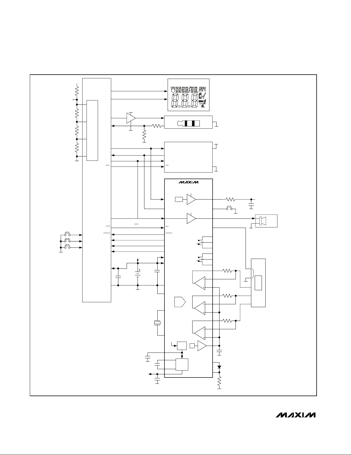
MAX1358/MAX1359/MAX1360
16-Bit Data-Acquisition Systems with ADC, DACs,
UPIOs, RTC, Voltage Monitors, and Temp Sensor
66 ______________________________________________________________________________________
V
CP
V
SS
LCDBIAS
LCD
DRIVERS
µC
DOWN
UP
MEM
V
SS
INPUT
INPUT
INPUT
V
SS
UPIO2
UPIO1
UPIO3
UPIO4
SNO1
SCM1
SNC1
SNO2
SCM2
SNC2
OUT1
IN1-
IN1+
OUT2
IN2-
IN2+
OUT3
IN3-
IN3+
AIN1
AIN2
REF
MAX1360
PWM
CPOUT
CPOUT
DIN
DOUT
SCLK
CS
RESET
INT
CLK
CLK32K
AV
DD
DV
DD
V
SS
TEST
STRIP
STRIP INSERTED
V
SS
PWRON
PIEZO
ALARM
V
SS
V
SS
LCDBIAS
V
SS
REMOTE TEMPERATUREMEASUREMENT DIODE
AGND
DGND
32KIN
32KOUT
ADC
BG
32.768kHz
LINEAR
REG
DV
DD
CHARGE-
PUMP
DOUBLER
V
SS
REG
CF+
CF-
CPOUT
V
SS
V
BAT
2 AAA OR
1 LITHIUM
COIN CELL
V
SS
V
SS
V
DD
FREQOUT
CS2
RESET
INPUT
X2IN
32KIN
EEPROM
V
SS
V
BAT
GND
V
CC
CS
SI
SCK
SO
SERIAL-PORT INTERFACE
V
SS
CS1
SCK
MISO
MOSI
V
SS
V
CP
V
SS
TXD
SEG<23:0>
COM<3:0>
RXD
V
CP
HIGH-FREQUENCY MICRO CLOCK
32kHz MICRO CLOCK
LCD GLA SS
CS2
Figure 28. MAX1360 Self-Biased Electrochemical Meter Application Circuit
Page 67

MAX1358/MAX1359/MAX1360
16-Bit Data-Acquisition Systems with ADC, DACs,
UPIOs, RTC, Voltage Monitors, and Temp Sensor
______________________________________________________________________________________ 67
V
CP
V
SS
LCDBIAS
LCD
DRIVERS
µC
DOWN
UP
MEM
V
SS
INPUT
INPUT
INPUT
UPIO2
UPIO1
UPIO3
UPIO4
OUTA
SWA
FBA
OUT1
IN1-
IN1+
AIN1
AIN2
REF
MAX1358
PWM
CPOUT
CPOUT
DIN
DOUT
SCLK
CS
RESET
INT
CLK
CLK32K
AV
DD
DV
DD
V
SS
TEST
STRIP
STRIP INSERTED
PIEZO
ALARM
V
SS
LCDBIAS
V
SS
REMOTE TEMPERATUREMEASUREMENT DIODE
AGND
DGND
32KIN
32KOUT
ADC
BG
32.768kHz
LINEAR
REG
DV
DD
CHARGE-
PUMP
DOUBLER
V
SS
REG
CF+
CF-
CPOUT
V
SS
V
BAT
2 AAA OR
1 LITHIUM
COIN CELL
V
SS
V
SS
V
DD
TXD
CS2
RESET
INPUT
EEPROM
V
SS
V
BAT
GND
V
CC
CS
SI
SCK
SO
SERIAL-PORT INTERFACE
V
SS
CS1
SCK
MISO
MOSI
V
SS
SEG<23:0>
COM<3:0>
RXD
V
CP
HIGH-FREQUENCY MICRO CLOCK
32kHz MICRO CLOCK
LCD GLA SS
BUZ_LO
BUZ_HI
RX_WAKEUP
RX_WAKEUP
SNO2
SCM2
SNC2
V
SS
DACA
OUTB
SWB
FBB
DACB
SNO1
SCM1
SNC1
CS2
X2IN
32KIN
Figure 29. MAX1358 Electrochemical Meter Application Circuit (Traditional and Counter Configuration)
Page 68

MAX1358/MAX1359/MAX1360
16-Bit Data-Acquisition Systems with ADC, DACs,
UPIOs, RTC, Voltage Monitors, and Temp Sensor
68 ______________________________________________________________________________________
ADC Calibration
Internal to the MAX1358/MAX1359/MAX1360, the ADC
is 24 bits and is always in bipolar mode. The OFFSET
CAL and GAIN CAL data are also 24 bits. The conversion to unipolar and the gain are performed digitally.
The default values for the OFFSET CAL and GAIN CAL
registers in the MAX1358/MAX1359/MAX1360 are
00 0000h and 80 0000h, respectively.
The calibration works as follows:
ADC = (RAW - OFFSET) x Gain x PGA
where ADC is the conversion result in the DATA register, RAW is the output of the decimation filter internal to
the MAX1358/MAX1359/MAX1360, OFFSET is the value
stored in the OFFSET CAL register, Gain is the value
stored in the GAIN CAL register, and PGA is the selected PGA gain found in the ADC register as GAIN<1:0>.
In unipolar mode, all negative values return a zero
result and an additional gain of 2 is added.
For self-calibration, the offset value is the RAW result
when the inputs are shorted internally and the gain value
is 1 / (RAW - OFFSET) with the reference connected to
the input. This is done automatically when these modes
are selected. The self offset and gain calibration corrects
for errors internal to the ADC and the results are stored
and used automatically in the OFFSET CAL and GAIN
CAL registers. For best results, use the ADC in the same
configuration as the calibration. This pertains to conversion rate only because the PGA gain and unipolar/bipolar modes are performed digitally.
For system calibration, the offset and gain values correct for errors in the whole signal path including the
internal ADC and any external circuits in the signal
path. For the system calibration, a user-provided zeroinput condition is required for the offset calibration and
a user-provided full-scale input is required for the gain
calibration. These values are automatically written to
the OFFSET CAL and GAIN CAL registers. The order of
the calibrations should be offset followed by gain.
The offset correction value is in two’s complement. The
default value is 000000h, 00...00b, or 0 decimal.
The gain correction value is an unsigned binary number with 23 bits to the right of the decimal point. The
largest number is therefore 1.1111...1b = 2 - 2
-23
and
the smallest is 0.000...0b = 0, although it does not
make sense to use a number smaller than 0.1000...0b
= 0.5. The default value is 800000h, 1.000...0b or 1
decimal.
Changing the offset or gain calibration values does not
affect the value in the DATA register until a new conversion has completed. This applies to all the mode bits
for PGA gain, unipolar/bipolar, etc.
Grounding and Layout
For best performance, use PC boards with separate
analog and digital ground planes.
Design the PC board so that the analog and digital sections are separated and confined to different areas of
the board. Join the digital and analog ground planes at
one point. If the DAS (MAX1358/MAX1359/MAX1360) is
the only device requiring an AGND-to-DGND connection, connect planes to the AGND pin of the DAS. In
systems where multiple devices require AGND-toDGND connections, the connection should still be
made at only one point. Make the star ground as close
to the MAX1358/MAX1359/MAX1360 as possible.
Avoid running digital lines under the device because
these may couple noise onto the device. Run the analog ground plane under the MAX1358/MAX1359/
MAX1360 to minimize coupling of digital noise. Make
the power-supply lines to the MAX1358/MAX1359/
MAX1360 as wide as possible to provide low-impedance paths and reduce the effects of glitches on the
power-supply line.
Shield fast-switching signals such as clocks with digital
ground to avoid radiating noise to other sections of the
board. Avoid running clock signals near the analog
inputs. Avoid crossover of digital and analog signals.
Good decoupling is important when using high-resolution ADCs. Decouple all analog supplies with 10µF
capacitors in parallel with 0.1µF HF ceramic capacitors
to AGND. Place these components as close to the
device as possible to achieve the best decoupling.
Crystal Layout
Follow basic layout guidelines when placing a crystal
on a PC board with a DAS to avoid coupled noise.
1) Place the crystal as close as possible to 32KIN and
32KOUT. Keeping the trace lengths between the
crystal and inputs as short as possible reduces the
probability of noise coupling by reducing the length
of the “antennae”. Keep the 32KIN and 32KOUT
lines close to each other to minimize the loop area
of the clock lines. Keeping the trace lengths short
also decreases the amount of stray capacitance.
2) Keep the crystal solder pads and trace width to
32KIN and 32KOUT as small as possible. The larger these bond pads and traces are, the more likely
it is that noise will couple from adjacent signals.
3) Place a guard ring (connect to ground) around the
crystal to isolate the crystal from noise coupled
from adjacent signals.
4) Ensure that no signals on other PC board layers run
directly below the crystal or below the traces to
Page 69

MAX1358/MAX1359/MAX1360
16-Bit Data-Acquisition Systems with ADC, DACs,
UPIOs, RTC, Voltage Monitors, and Temp Sensor
______________________________________________________________________________________ 69
32KIN and 32KOUT. The more the crystal is isolated from other signals on the board, the less likely it
is that noise will be coupled into the crystal.
Maintain a minimum distance of 5mm between any
digital signal and any trace connected to 32KIN or
32KOUT.
5) Place a local ground plane on the PC board layer
immediately below the crystal guard ring. This
helps to isolate the crystal from noise coupling from
signals on other PC board layers.
Note: The ground plane must be in the vicinity of the
crystal only and not on the entire board.
AV = 1, 1.638, 2
MAX1360
C
REF
REF
R
R
R
R
B
R
A
R
D
R
C
R
2N3904
1.25V
REF
AIN2
IN1+
IN1-
AGND
OUT1
IN3+
OUT3
IN3-
OUT2
IN2+
AV
DD
IN2-
AIN1
Figure 31. Strain-Gauge Measurement with Remote
Temperature Sensor
AV = 1, 2, 4, 8
A
V
= 1, 1.638, 2
MAX1358
MAX1359
MAX1360
PGA
MUX
2N3904
16-BIT ADC
C
REF
REF
REF
MUX
TEMP
SENSOR
AIN1
AGND
AIN2
AGND
2N3904
1.25V
REF
Figure 30. Temperature Measurement with Two Remote Sensors
MAX1359
MAX1360
R
3
R
2
R
2
R
3
R
1
R
1
IN1+
IN1-
SCM1
V
OUT
SCM2
OUT1
SNO1
SNC1
SNO2
SNC2
V
IN+
V
IN-
OUT2
IN2+
IN2-
Figure 32. Programmable-Gain Instrumentation Amplifier
Page 70

MAX1358/MAX1359/MAX1360
16-Bit Data-Acquisition Systems with ADC, DACs,
UPIOs, RTC, Voltage Monitors, and Temp Sensor
70 ______________________________________________________________________________________
Parameter Definitions
INL
Integral nonlinearity (INL) is the deviation of the values
on an actual transfer function from a straight line. This
straight line is either a best-straight-line fit or a line
drawn between the endpoints of the transfer function,
once offset and gain errors have been nulled. INL for
the MAX1358/MAX1359/MAX1360 is measured using
the endpoint method.
DNL
Differential nonlinearity (DNL) is the difference between
an actual step width and the ideal value of 1 LSB. A DNL
error specification of greater than -1 LSB guarantees no
missing codes and a monotonic transfer function.
Gain Error
Gain error is the amount of deviation between the measured full-scale transition point and the ideal full-scale
transition point.
REF
SNO1
SCM1
SNC1
AGND
SPDT1
PWM
IN1+
IN1-
OUT1
TRANSDUCER
0.300V (±1mV)
I
T
0.1µF
60kΩ
~0.3V
240kΩ
350kΩ
~19kHz
VOLTAGE
RIPPLE <1mV
~1.25V
MAX1360
Figure 34. Sensor-Bias Voltage Trim Application
MAX1358
MAX1359
MAX1360
(1.8V
TO
2.6V)
0.01µF
µC
MUX
SV_
ALH_
UPIO_
LCD
DRIVERS
SEG
LCD
COMnm
CPOUT
200kΩ
100kΩ
100kΩ
100kΩ
100kΩ
PWM
DV
DD
CPOUT
EN_
Figure 33. LCD Contrast-Adjustment Application
Page 71

MAX1358/MAX1359/MAX1360
16-Bit Data-Acquisition Systems with ADC, DACs,
UPIOs, RTC, Voltage Monitors, and Temp Sensor
______________________________________________________________________________________ 71
Common-Mode Rejection
Common-mode rejection (CMR) is the ability of a
device to reject a signal that is common to both input
terminals. The common-mode signal can be either an
AC or a DC signal or a combination of the two. CMR is
often expressed in decibels.
Power-Supply Rejection Ratio (PSRR)
Power-supply rejection ratio (PSRR) is the ratio of the
input supply change (in volts) to the change in the
converter output (in volts). It is typically measured in
decibels.
Chip Information
PROCESS: BiCMOS
SHDN
PWM
ALH_
UPIO_
SV_
DV
DD
CPOUT
MUX
MAX1358
MAX1359
MAX1360
V
IN
VOUT
POWER SUPPLY
AV
DD
V
DD
µC
100µF
<10µA
V
DD
PSCTL
V
BATT
DV
DD
ON-TIME <100ms TYP
10s PERIOD TYP
+3.3V
V
DD
+2.3V
PSCTL
EN_
10MΩ
Figure 35. Power-Supply Sleep-Mode Duty-Cycle Control
PWM
ALH_
UPIO_
SV_
DV
DD
CPOUT
MUX
1kΩ
0V
CPOUT(+3.2V)
1 TO 8kHz TYP
~10,000pF
MAX1358
MAX1359
MAX1360
Figure 36. Single-Ended Piezoelectric Buzzer Drive
Page 72
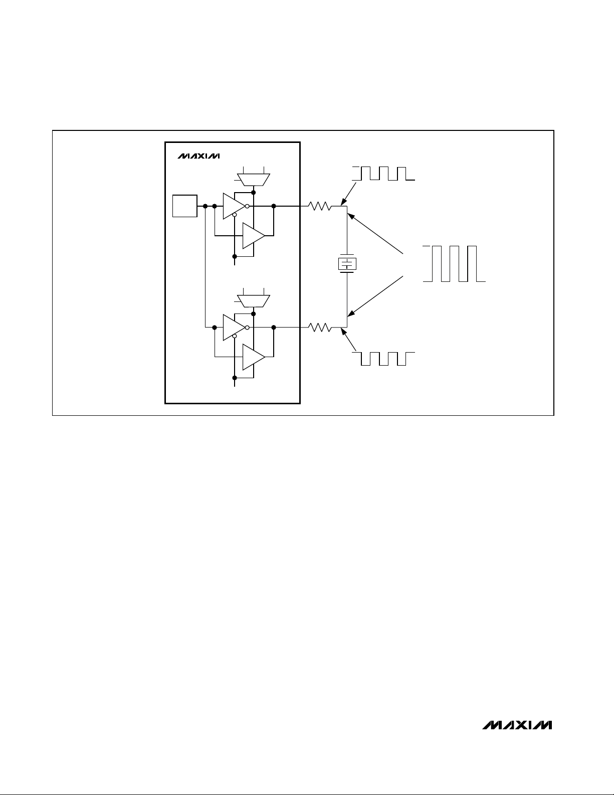
MAX1358/MAX1359/MAX1360
16-Bit Data-Acquisition Systems with ADC, DACs,
UPIOs, RTC, Voltage Monitors, and Temp Sensor
72 ______________________________________________________________________________________
MAX1358
MAX1359
MAX1360
MUX
SV_
ALH_
UPIO_
1kΩ
PWM
DV
DD
CPOUT
MUX
SV_
ALH_
UPIO_
1kΩ
DV
DD
CPOUT
0V
0V
CPOUT(+3.2V)
CPOUT
+
6.4V DIFF
-
-CPOUT
CPOUT(~+3.2V)
1 TO 8kHz TYP
1 TO 8kHz TYP
~10,000pF
Figure 37. Differential Piezoelectric Buzzer Drive
Page 73

MAX1358/MAX1359/MAX1360
16-Bit Data-Acquisition Systems with ADC, DACs,
UPIOs, RTC, Voltage Monitors, and Temp Sensor
______________________________________________________________________________________ 73
40
39
38
37
36
35
34
33
32
31
21 22 23 24 25 26 27 28 29 30
CPOUT
IN1+
IN1-
OUTB
SWB
SWA
FBA
OUTA
AGND
FBB
AIN2
AIN1
REF
REG
AV
DD
CF-
CF+
DV
DD
DGND
UPIO1
11
12
13
14
15
16
17
18
19
20
10 9 8 7 6 5 4 3 2 1
CLK
UPIO2
UPIO3
UPIO4
DOUT
SCLK
DIN
INT
CLK32K
32KOUT
32KIN
SNO1
SCM1
SNC1
OUT1
SNC2
SCM2
SNO2
MAX1358
CS
RESET
TQFN
Pin Configurations
40
39
38
37
36
35
34
33
32
31
21 22 23 24 25 26 27 28 29 30
CPOUT
IN1+
IN1-
OUT2
IN2+
SWA
FBA
OUTA
AGND
IN2-
AIN2
AIN1
REF
REG
AV
DD
CF-
CF+
DV
DD
DGND
UPIO1
11
12
13
14
15
16
17
18
19
20
10 9 8 7 6 5 4 3 2 1
CLK
UPIO2
UPIO3
UPIO4
DOUT
SCLK
DIN
INT
CLK32K
32KOUT
32KIN
SNO1
SCM1
SNC1
OUT1
SNC2
SCM2
SNO2
MAX1359
CS
RESET
TQFN
40
39
38
37
36
35
34
33
32
31
21 22 23 24 25 26 27 28 29 30
CPOUT
IN1+
IN1-
OUT2
IN2+
IN3+
IN3-
OUT3
AGND
IN2-
AIN2
AIN1
REF
REG
AV
DD
CF-
CF+
DV
DD
DGND
UPIO1
11
12
13
14
15
16
17
18
19
20
10 9 8 7 6 5 4 3 2 1
CLK
UPIO2
UPIO3
UPIO4
DOUT
SCLK
DIN
INT
CLK32K
32KOUT
32KIN
SNO1
SCM1
SNC1
OUT1
SNC2
SCM2
SNO2
MAX1360
CS
RESET
TQFN
Page 74

MAX1358/MAX1359/MAX1360
16-Bit Data-Acquisition Systems with ADC, DACs,
UPIOs, RTC, Voltage Monitors, and Temp Sensor
Maxim cannot assume responsibility for use of any circuitry other than circuitry entirely embodied in a Maxim product. No circuit patent licenses are
implied. Maxim reserves the right to change the circuitry and specifications without notice at any time.
74 ____________________Maxim Integrated Products, 120 San Gabriel Drive, Sunnyvale, CA 94086 408-737-7600
© 2005 Maxim Integrated Products Printed USA is a registered trademark of Maxim Integrated Products, Inc.
Package Information
(The package drawing(s) in this data sheet may not reflect the most current specifications. For the latest package outline information,
go to www.maxim-ic.com/packages
.)
QFN THIN 6x6x0.8.EPS
e e
LL
A1 A2
A
E/2
E
D/2
D
E2/2
E2
(NE-1) X e
(ND-1) X e
e
D2/2
D2
b
k
k
L
C
L
C
L
C
L
C
L
E
1
2
21-0141
PACKAGE OUTLINE
36, 40, 48L THIN QFN, 6x6x0.8mm
L1
L
e
8. COPLANARITY APPLIES TO THE EXPOSED HEAT SINK SLUG AS WELL AS THE TERMINALS.
6. ND AND NE REFER TO THE NUMBER OF TERMINALS ON EACH D AND E SIDE RESPECTIVELY.
5. DIMENSION b APPLIES TO METALLIZED TERMINAL AND IS MEASURED BETWEEN 0.25 mm AND 0.30 mm
FROM TERMINAL TIP.
4. THE TERMINAL #1 IDENTIFIER AND TERMINAL NUMBERING CONVENTION SHALL CONFORM TO JESD 95-1
SPP-012. DETAILS OF TERMINAL #1 IDENTIFIER ARE OPTIONAL, BUT MUST BE LOCATED WITHIN THE
ZONE INDICATED. THE TERMINAL #1 IDENTIFIER MAY BE EITHER A MOLD OR MARKED FEATURE.
9. DRAWING CONFORMS TO JEDEC MO220, EXCEPT FOR 0.4mm LEAD PITCH PACKAGE T4866-1.
7. DEPOPULATION IS POSSIBLE IN A SYMMETRICAL FASHION.
3. N IS THE TOTAL NUMBER OF TERMINALS.
2. ALL DIMENSIONS ARE IN MILLIMETERS. ANGLES ARE IN DEGREES.
1. DIMENSIONING & TOLERANCING CONFORM TO ASME Y14.5M-1994.
NOTES:
10. WARPAGE SHALL NOT EXCEED 0.10 mm.
E
2
2
21-0141
PACKAGE OUTLINE
36, 40, 48L THIN QFN, 6x6x0.8mm
 Loading...