

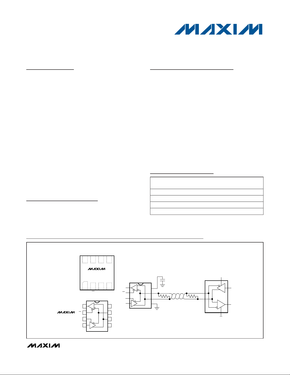
General Description
The MAX13485E/MAX13486E +5V, half-duplex, ±15kV
ESD-protected RS-485 transceivers feature one driver
and one receiver. These devices include fail-safe circuitry,
guaranteeing a logic-high receiver output when receiver
inputs are open or shorted. The receiver outputs a logichigh if all transmitters on a terminated bus are disabled
(high impedance). The MAX13485E/MAX13486E include
a hot-swap capability to eliminate false transitions on the
bus during power-up or live-insertion.
The MAX13485E features reduced slew-rate drivers
that minimize EMI and reduce reflections caused by
improperly terminated cables, allowing error-free transmission up to 500kbps. The MAX13486E driver slew
rate is not limited, allowing transmit speeds up to
16Mbps.
The MAX13485E/MAX13486E feature a 1/4-unit load
receiver input impedance, allowing up to 128 transceivers
on the bus. These devices are intended for half-duplex
communications. All driver outputs are protected to ±15kV
ESD using the Human Body Model. The MAX13485E/
MAX13486E are available in 8-pin SO and space-saving
8-pin µDFN packages. The devices operate over the
extended -40°C to +85°C temperature range.
Applications
Utility Meters
Industrial Controls
Industrial Motor Drives
Automated HVAC Systems
Features
♦ +5V Operation
♦ True Fail-Safe Receiver While Maintaining
EIA/TIA-485 Compatibility
♦ Hot-Swappable for Telecom Applications
♦ Enhanced Slew-Rate Limiting Facilitates Error-
Free Data Transmission (MAX13485E)
♦ High-Speed Version (MAX13486E) Allows for
Transmission Speeds Up to 16Mbps
♦ Extended ESD Protection for RS-485/RS-422 I/O
Pins ±15kV Using Human Body Model
♦ 1/4 Unit Load, Allowing Up to 128 Transceivers on
the Bus
♦ Available in Space-Saving 8-Pin μDFN or Industry
Standard 8-Pin SO Packages
MAX13485E/MAX13486E
Half-Duplex RS-485/RS-422 Transceivers in µDFN
________________________________________________________________
Maxim Integrated Products
1
19-0742; Rev 0; 1/07
For pricing, delivery, and ordering information, please contact Maxim/Dallas Direct! at
1-888-629-4642, or visit Maxim’s website at www.maxim-ic.com.
Ordering Information/
Selector Guide
+
Denotes a lead-free package.
Note: All devices are specified over the -40°C to +85°C operating
temperature range.
Rt
RE
RO
B
A
A
B
Rt
R
D
RO
DI
8
7
6
5
1
2
3
4
RE
DE
R
DI
D
DE
+
123
87465
V
CC
A GNDB
RO DIDERE
MAX13485E
MAX13486E
DFN
+
A
GNDDI
1
2
87V
CC
BRE
DE
RO
SO
SO
3
4
6
5
R
D
+
TOP VIEW
GND
V
CC
0.1μF
MAX13485E
MAX13486E
Pin Configurations
PART
PINPACKAGE
MAX13485EELA+T 8 µDFN Yes L822-1
MAX13485EESA+ 8 SO Yes S8-2
MAX13486EELA+T 8 µDFN No L822-1
MAX13486EESA+ 8 SO No S8-2
SLEW-RATE
LIMITED
PKG
CODE
MAX13485E/MAX13486E
Half-Duplex RS-485/RS-422 Transceivers in µDFN
2 _______________________________________________________________________________________
ABSOLUTE MAXIMUM RATINGS
Stresses beyond those listed under “Absolute Maximum Ratings” may cause permanent damage to the device. These are stress ratings only, and functional
operation of the device at these or any other conditions beyond those indicated in the operational sections of the specifications is not implied. Exposure to
absolute maximum rating conditions for extended periods may affect device reliability.
(All voltages referenced to GND.)
V
CC
........................................................................................+6V
DE, RE, DI.................................................................-0.3V to +6V
A, B ..............................................................................-8V to 13V
Short-Circuit Duration (RO, A, B) to GND ..................Continuous
Continuous Power Dissipation (T
A
= +70°C)
8-Pin SO (derate 5.9mW/°C above +70°C)..................471mW
8-Pin µDFN (derate 4.8mW/°C above +70°C) ..........380.6mW
Operating Temperature Range ...........................-40°C to +85°C
Junction Temperature......................................................+150°C
Storage Temperature Range .............................-65°C to +150°C
Lead Temperature (soldering, 10s) .................................+300°C
ELECTRICAL CHARACTERISTICS
(VCC= +5V ±5%, TA= T
MIN
to T
MAX
, unless otherwise noted. Typical values are at VCC= +5V and TA= +25°C.) (Notes 1, 2)
PARAMETER SYMBOL CONDITIONS MIN TYP MAX UNITS
DRIVER
Change in Magnitude of
Differential Output Voltage
Driver Common-Mode Output
Voltage
Change in Magnitude of
Common-Mode Voltage
Input-High Voltage V
Input-Low Voltage V
Input Current I
Driver Short-Circuit Output
Current (Note 4)
Driver Short-Circuit Foldback
Output Current Note 3)
RECEIVER
Input Current (A and B) I
Receiver-Differential-Threshold
Voltage
Receiver Input Hysteresis ΔV
Output-High Voltage V
R
= 100Ω, Figure 1 2.0 V
DIFF
R
= 54Ω, Figure 1 1.5Differential Driver Output V
OD
DIFF
No load V
R
ΔV
V
OC
ΔV
IN
I
OSD
I
OSDF
A, B
V
TH
OH
OD
OC
IH
IL
TH
= 100Ω or 54Ω, Figure 1 (Note 3) 0.2 V
DIFF
R
= 100Ω or 54Ω, Figure 1
DIFF
R
= 100Ω or 54Ω, Figure 1 (Note 3) 0.2 V
DIFF
DI, DE, RE 2.0 V
DI, DE, RE 0.8 V
DI, DE, RE ±1 µA
0V < V
-7V < V
< +12V +50 +250
OUT
OUT
(VCC - 1V) < V
-7V < V
OUT
DE = GND, VCC = GND
or +5V
-7V < VCM < +12V -200 -50 mV
VA + VB = 0V 25 mV
IO = -1.6mA, VA - VB > V
CC
CC
V
CC
/ 2
3V
< 0V -250 -50
< +12V 20
OUT
< 0V -20
VIN = +12V 250
= -7V -200
V
IN
V
-
TH
CC
1.5
V
mA
mA
µA
V
MAX13485E/MAX13486E
Half-Duplex RS-485/RS-422 Transceivers in µDFN
_______________________________________________________________________________________ 3
ELECTRICAL CHARACTERISTICS (continued)
(VCC= +5V ±5%, TA= T
MIN
to T
MAX
, unless otherwise noted. Typical values are at VCC= +5V and TA= +25°C.) (Notes 1, 2)
SWITCHING CHARACTERISTICS—MAX13485E
(VCC= +5V ±5%, TA= T
MIN
to T
MAX
, unless otherwise noted. Typical values are at VCC= +5V and TA= +25°C.) (Note 1)
)
)
PARAMETER SYMBOL CONDITIONS MIN TYP MAX UNITS
Output-Low Voltage V
Tri-State Output Current at
Receiver
Receiver Input Resistance R
Receiver-Output Short-Circuit
Current
POWER SUPPLY
Supply Voltage V
Supply Current I
Shutdown Supply Current I
ESD PROTECTION
ESD Protection (A, B)
ESD Protection (All Other Pins) Human Body Model ±2 kV
IO = 1mA, VA - VB < -V
OL
I
OZR
IN
I
OSR
CC
CC
SHDN
0V < VO < V
CC
-7V < VCM < +12V 48 kΩ
0V < V
RO
< V
CC
DE = 1, RE = 0, no load 4.5 mA
DE = 0, RE = 1 10 µA
TH
±7 ±95 mA
4.75 5.25 V
Air Gap Discharge IEC61000-4-2
(MAX13485E)
Human Body Model ±15
0.4 V
±1 µA
±15
PARAMETER SYMBOL CONDITIONS MIN TYP MAX UNITS
DRIVER
Driver Propagation Delay
Driver-Differential Output Rise or
Fall Time
Driver-Differential Output Skew
- t
|t
DPLH
DPHL
|
Maximum Data Rate 500 kbps
Driver Enable to Output High t
Driver Enable to Output Low t
Driver Disable Time from High t
Driver Disable Time from Low t
Driver Enable from Shutdown to
Output High
Driver Enable from Shutdown to
Output Low
Time to Shutdown t
RECEIVER
Receiver Propagation Delay
Receiver Output Skew t
Maximum Data Rate 500 kbps
t
DPLH
t
DPHL
t
HL
t
LH
t
DSKEWRDIFF
DZH
DZL
DHZ
DLZ
t
DZH(SHDN
t
DZL(SHDN
SHDN
t
RPLH
t
RPHL
RSKEW
R
= 54Ω, CL = 50pF, Figures 2 and 3
DIFF
R
= 54Ω, CL = 50pF, Figures 2 and 3
DIFF
= 54Ω, CL = 50pF, Figures 2 and 3 140 ns
Figures 4 and 5 2500 ns
Figures 4 and 5 2500 ns
Figures 4 and 5 100 ns
Figures 4 and 5 100 ns
Figures 4 and 5 5500 ns
Figures 4 and 5 5500 ns
CL = 15pF, Figures 6 and 7
CL = 15pF, Figure 7 13 ns
200 1000
200 1000
250 900
250 900
50 340 700 ns
80
80
kV
ns
ns
ns
MAX13485E/MAX13486E
Half-Duplex RS-485/RS-422 Transceivers in µDFN
4 _______________________________________________________________________________________
SWITCHING CHARACTERISTICS—MAX13485E (continued)
(VCC= +5V ±5%, TA= T
MIN
to T
MAX
, unless otherwise noted. Typical values are at VCC= +5V and TA= +25°C.) (Note 1)
)
)
SWITCHING CHARACTERISTICS—MAX13486E
(VCC= +5V ±5%, TA= T
MIN
to T
MAX
, unless otherwise noted. Typical values are at VCC= +5V and TA= +25°C.) (Note 1)
)
)
PARAMETER SYMBOL CONDITIONS MIN TYP MAX UNITS
Receiver Enable to Output High t
Receiver Enable to Output Low t
Receiver Disable Time from High t
Receiver Disable Time from Low t
Receiver Enable from Shutdown
to Output High
Receiver Enable from Shutdown
to Output Low
Time to Shutdown t
DRIVER
Driver Propagation Delay
Driver Differential Output Rise or
Fall Time
Differential Driver Output Skew
|t
DPLH
Maximum Data Rate 16 Mbps
Driver Enable to Output High t
Driver Enable to Output Low t
Driver Disable Time from High t
Driver Disable Time from Low t
Driver Enable from Shutdown to
Output High
Driver Enable from Shutdown to
Output Low
Time to Shutdown t
RECEIVER
Receiver Propagation Delay
Receiver Output Skew t
Maximum Data Rate 16 Mbps
PARAMETER SYMBOL CONDITIONS MIN TYP MAX UNITS
- t
|
DPHL
RZH
RZL
RHZ
RLZ
t
RZH(SHDN
t
RZL(SHDN
SHDN
t
DPLH
t
DPHL
t
HL
t
LH
t
DSKEWRDIFF
DZH
DZL
DHZ
DLZ
t
DZH(SHDN
t
DZL(SHDN
SHDN
t
RPLH
t
RPHL
RSKEW
Figure 8 50 ns
Figure 8 50 ns
Figure 8 50 ns
Figure 8 50 ns
Figure 8 2200 ns
Figure 8 2200 ns
50 340 700 ns
R
= 54Ω, CL = 50pF, Figures 2 and 3
DIFF
R
= 54Ω, CL = 50pF, Figures 2 and 3
DIFF
= 54Ω, CL = 50pF, Figures 2 and 3 8 ns
Figures 4 and 5 50 ns
Figures 4 and 5 50 ns
Figures 4 and 5 50 ns
Figures 4 and 5 50 ns
Figures 4 and 5 2200 ns
Figures 4 and 5 2200 ns
50 340 700 ns
CL = 15pF, Figures 6 and 7
CL = 15pF, Figure 7 13 ns
50
50
15
15
80
80
ns
ns
ns
MAX13485E/MAX13486E
Half-Duplex RS-485/RS-422 Transceivers in µDFN
_______________________________________________________________________________________ 5
SWITCHING CHARACTERISTICS—MAX13486E (continued)
(VCC= +5V ±5%, TA= T
MIN
to T
MAX
, unless otherwise noted. Typical values are at VCC= +5V and TA= +25°C.) (Note 1)
)
)
Note 1: µDFN devices production tested at +25°C. Overtemperature limits are generated by design.
Note 2: All currents into the device are positive. All currents out of the device are negative. All voltages referred to device ground,
unless otherwise noted.
Note 3: ΔV
OD
and ΔVOCare the changes in VODand VOCwhen the DI input changes states.
Note 4: The short-circuit output current applied to peak current just prior to foldback current limiting. The short-circuit foldback
output current applies during current limiting to allow a recovery from bus contention.
Typical Operating Characteristics
(VCC= +5V, TA = +25°C, unless otherwise noted.)
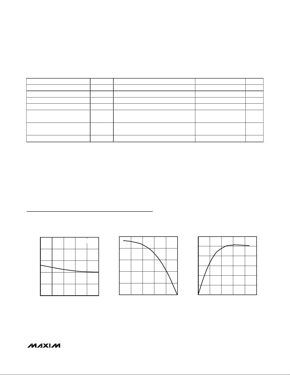
3.0
3.2
3.6
3.4
3.8
4.0
-40 10-15 35 60 85
SUPPLY CURRENT vs. TEMPERATURE
MAX13485-86E toc01
TEMPERATURE (°C)
SUPPLY CURRENT (mA)
NO LOAD
0
7
21
14
28
35
021345
OUTPUT CURRENT vs. RECEIVER
OUTPUT HIGH VOLTAGE
MAX13485-86E toc02
OUTPUT HIGH VOLTAGE (V)
OUTPUT CURRENT (mA)
0
20
10
40
30
50
60
021345
OUTPUT CURRENT vs. RECEIVER
OUTPUT LOW VOLTAGE
MAX13485-86E toc03
OUTPUT LOW VOLTAGE (V)
OUTPUT CURRENT (mA)
PARAMETER SYMBOL CONDITIONS MIN TYP MAX UNITS
Receiver Enable to Output High t
Receiver Enable to Output Low t
Receiver Disable Time from High t
Receiver Disable Time from Low t
Receiver Enable from Shutdown
to Output High
Receiver Enable from Shutdown
to Output Low
Time to Shutdown t
RZH
RZL
RHZ
RLZ
t
RZH(SHDN
t
RZL(SHDN
SHDN
Figure 8 50 ns
Figure 8 50 ns
Figure 8 50 ns
Figure 8 50 ns
Figure 8 2200 ns
Figure 8 2200 ns
50 340 700 ns

MAX13485E/MAX13486E
Half-Duplex RS-485/RS-422 Transceivers in µDFN
6 _______________________________________________________________________________________
Typical Operating Characteristics (continued)
(VCC= +5V, TA = +25°C, unless otherwise noted.)
4.0
4.4
4.2
4.8
4.6
5.2
5.0
5.4
-40 10-15 35 60 85
RECEIVER OUTPUT HIGH
VOLTAGE vs. TEMPERATURE
MAX13485-86E toc04
TEMPERATURE (°C)
OUTPUT HIGH VOLTAGE (V)
IO = 1mA
0
0.1
0.3
0.2
0.4
0.5
-40 10-15 35 60 85
RECEIVER OUTPUT LOW
VOLTAGE vs. TEMPERATURE
MAX13485-86E toc05
TEMPERATURE (°C)
OUTPUT LOW VOLTAGE (V)
IO = 1mA
DIFFERENTIAL OUPUT CURRENT
vs. DIFFERENTIAL OUTPUT VOLTAGE
MAX13485-86E toc06
OUTPUT VOLTAGE (V)
OUTPUT CURRENT (mA)
4321
20
40
60
80
0
05
0
1.0
0.5
2.0
1.5
2.5
3.0
-40 10-15 35 60 85
DRIVER-DIFFERENTIAL OUTPUT
VOLTAGE vs. TEMPERATURE
MAX13485-86E toc07
TEMPERATURE (°C)
DIFFERENTIAL OUTPUT VOLTAGE (V)
R
DIFF
= 54Ω
0
40
20
80
60
100
120
-7 -5 -4 -3-6 -2 0-1 12345
OUTPUT CURRENT vs. TRANSMITTER
OUTPUT HIGH VOLTAGE
MAX13485-86E toc08
OUTPUT HIGH VOLTAGE (V)
OUTPUT CURRENT (mA)
0
40
20
80
60
100
120
0462 8 10 12
OUTPUT CURRENT vs. TRANSMITTER
OUTPUT LOW VOLTAGE
MAX13485-86E toc09
OUTPUT LOW VOLTAGE (V)
OUTPUT CURRENT (mA)
0
3
2
1
4
5
6
7
8
9
10
-40 10-15 35 60 85
SHUTDOWN CURRENT
vs. TEMPERATURE
MAX13485-86E toc10
TEMPERATURE (°C)
SHUTDOWN CURRENT (μA)
300
400
350
500
450
550
600
-40 10-15 35 60 85
DRIVER PROPAGATION
vs. TEMPERATURE (MAX13485E)
MAX13485-86E toc11
TEMPERATURE (°C)
DRIVER PROPAGATION DELAY (ns)
t
DPLH
t
DPHL
0
10
5
20
15
25
30
-40 10-15 35 60 85
DRIVER PROPAGATION DELAY
vs. TEMPERATURE (MAX13486E)
MAX13485-86E toc12
TEMPERATURE (°C)
DRIVER PROPAGATION DELAY (ns)
t
DPLH
t
DPHL

MAX13485E/MAX13486E
Half-Duplex RS-485/RS-422 Transceivers in µDFN
_______________________________________________________________________________________
7
Typical Operating Characteristics (continued)
(VCC= +5V, TA = +25°C, unless otherwise noted.)
RECEIVER PROPAGATION
vs. TEMPERATURE (MAX13485E)
80
60
40
PROPAGATION DELAY (ns)
20
0
-40 85
t
RPHL
t
RPLH
TEMPERATURE (°C)
603510-15
MAX13485-86E toc13
RECEIVER PROPAGATION (ns)
DRIVER PROPAGATION (16Mbps)
(MAX13486E)
MAX13485/86E toc16
RECEIVER PROPAGATION
vs. TEMPERATURE (MAX13486E)
40
30
t
RPLH
20
10
0
-40 85
t
RPHL
TEMPERATURE (°C)
603510-15
RECEIVER PROPAGATION (16Mbps)
DI
2V/div
MAX13485-86E toc14
DRIVER PROPAGATION (500kbps)
(MAX13485E)
400ns/div
(MAX13486E)
MAX13485/86E toc17
B
2V/div
MAX13485/86E toc15
DI
2V/div
A-B
5V/div
10ns/div
A-B
5V/div
10ns/div
A
2V/div
RO
2V/div

MAX13485E/MAX13486E
Half-Duplex RS-485/RS-422 Transceivers in µDFN
8 _______________________________________________________________________________________
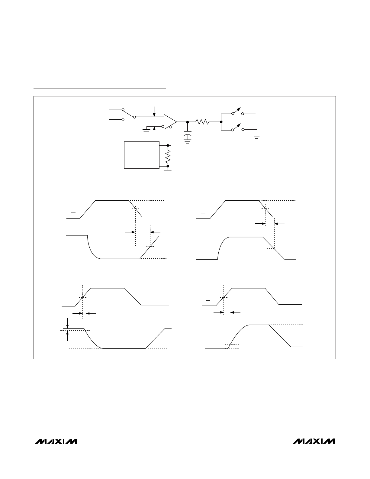
Figure 1. Driver DC Test Load
Figure 2. Driver Timing Test Circuit
Figure 3. Driver Propagation Delays
Test Circuits and Waveforms
A
R
DIFF
2
V
OD
B
C
L
R
DIFF
2
V
OC
V
CC
DI
0
B
A
1/2 V
V
O
V
O
V
0
DIFF
-V
O
10%
LH
1.5V
O
f = 1MHz, tLH ≤ 3ns, tHL ≤ 3ns
t
DPLH
90%
t
DSKEW
5V
DE
A
DI
B
1.5V
t
DPHL
V
= V(A) - V(B)
DIFF
90%
t
HLt
= |t
- t
DPHL
|
DPLH
V
ID
10%
1/2 V
R
DIFF
O
C
L

MAX13485E/MAX13486E
Half-Duplex RS-485/RS-422 Transceivers in µDFN
_______________________________________________________________________________________ 9
Figure 4. Driver Enable and Disable Times
Figure 6. Receiver Propagation Delay Test Circuit
Figure 5. Driver-Enable and -Disable-Timing Test Load
Figure 7. Receiver Propagation Delays
Test Circuits and Waveforms (continued)
V
CC
DE
0
A, B
V
OL
A, B
0
OUTPUT
UNDER TEST
500Ω
C
L
1.5V
t
DZL(SHDN),tDZL
2.3V
2.3V
V
S1
CC
OUTPUT NORMALLY LOW
OUTPUT NORMALLY HIGH
t
DZH(SHDN),tDZH
ATE
t
t
DHZ
DLZ
1.5V
V
+ 0.5V
OL
+ 0.5V
V
OH
B
V
ID
R
A
RECEIVER
OUTPUT
S2
A
B
V
OH
RO
V
OL
1.5V
f = 1MHz, t
t
RPHL
≤ 3ns, tHL ≤ 3ns
LH
t
RPLH
1.5V
= |t
- t
RPHL
RPLH
|
t
RSKEW
1V
-1V

MAX13485E/MAX13486E
Half-Duplex RS-485/RS-422 Transceivers in µDFN
10 ______________________________________________________________________
Pin Description
Function Tables
X = Don’t care, shutdown mode, driver, and receiver outputs
are in high impedance.
PIN NAME FUNCTION
1 RO Receiver Output
Receiver Output Enable. Drive RE low to enable RO. RO is high impedance when RE is high. Drive
2 RE
3DE
RE high and DE low to enter low-power shutdown mode. RE is a hot-swap input (see the Hot-Swap
Capability section for more details).
Driver Output Enable. Drive DE high to enable the driver outputs. These outputs are high-impedance
when DE is low. Drive RE high and DE low to enter low-power shutdown mode. DE is a hot-swap input
(see the Hot-Swap Capability section for more details).
4DI
5 GND Ground
6 A Noninverting Receiver Input and Noninverting Driver Output
7 B Inverting Receiver Input and Inverting Driver Output
8VCCPositive Supply, VCC = +5V ±5%. Bypass VCC to GND with a 0.1µF capacitor.
Driver Input. Drive DI low to force noninverting output low and inverting output high. Drive DI high to
force noninverting output high and inverting output low (see the Function Tables).
TRANSMITTING
INPUT OUTPUT
RE DE DI B A
X11 0 1
X10 1 0
0 0 X HIGH IMPEDANCE HIGH IMPEDANCE
1 0 X SHUTDOWN
RECEIVING
INPUT OUTPUT
RE DE A-B RO
0X > -50mV 1
0X < -200mV 0
0 X OPEN/SHORT 1
1 1 X HIGH IMPEDANCE
1 0 X SHUTDOWN
MAX13485E/MAX13486E
Half-Duplex RS-485/RS-422 Transceivers in µDFN
__________________________________________________________________________
Figure 8. Receiver Enable and Disable Times
Test Circuits and Waveforms (continued)
+1V
-1V
S1 OPEN
S2 CLOSED
S3 = +1V
RE
RO
S3
GENERATOR
t
RZH
V
CC
, t
RZH(SHDN)
1kΩ
CL
15pF
RE
RO
V
ID
50Ω
V
CC
/2
0
V
OH
V
/2
OH
0
S1
S2
S1 CLOSED
S2 OPEN
S3 = -1V
V
CC
V
CC
VCC/2
0
t
, t
RZL
RZL(SHDN)
V
CC
(VOL + VCC)/2
V
OL
S1 OPEN
S2 CLOSED
S3 = +1V
VCC/2
RE
t
RHZ
RO
0.25V
S1 CLOSED
S2 OPEN
VCC/2
S3 = -1V
t
RLZ
0.25V
V
CC
0
V
OH
0
RE
RO
V
CC
0
V
CC
V
OL

MAX13485E/MAX13486E
Detailed Description
The MAX13485E/MAX13486E half-duplex, high-speed
transceivers for RS-485/RS-422 communication contain
one driver and one receiver. These devices feature failsafe circuitry that guarantees a logic-high receiver output when receiver inputs are open or shorted, or when
they are connected to a terminated transmission line
with all drivers disabled (see the
Fail-Safe
section). The
MAX13485E/MAX13486E also feature a hot-swap capability allowing line insertion without erroneous data
transfer (see the
Hot-Swap Capability
section). The
MAX13485E features reduced slew-rate drivers that
minimize EMI and reduce reflections caused by
improperly terminated cables, allowing error-free transmission up to 500kbps. The MAX13486E driver slew
rate is not limited, making transmit speeds up to
16Mbps possible.
Fail-Safe
The MAX13485E/MAX13486E guarantee a logic-high
receiver output when the receiver inputs are shorted or
open, or when they are connected to a terminated
transmission line with all drivers disabled. This is done by
setting the receiver input threshold between -50mV and
-200mV. If the differential receiver input voltage (A - B) is
greater than or equal to -50mV, RO is logic-high. If (A - B)
is less than or equal to -200mV, RO is logic-low. In the
case of a terminated bus with all transmitters disabled,
the receiver’s differential input voltage is pulled to 0V by
the termination. With the receiver thresholds of the
MAX13485E/MAX13486E, this results is a logic-high with
a 50mV minimum noise margin. Unlike previous fail-safe
devices, the -50mV to -200mV threshold complies with
the ±200mV EIA/TIA-485 standard.
Hot-Swap Capability
Hot-Swap Inputs
When circuit boards are inserted into a hot or powered
backplane, differential disturbances to the data bus
can lead to data errors. Upon initial circuit-board insertion, the data communication processor undergoes its
own power-up sequence. During this period, the
processor’s logic-output drivers are high impedance
and are unable to drive the DE and RE inputs of these
devices to a defined logic level. Leakage currents up to
±10µA from the high impedance state of the processor’s logic drivers could cause standard CMOS enable
inputs of a transceiver to drift to an incorrect logic level.
Additionally, parasitic circuit-board capacitance could
cause coupling of VCCor GND to the enable inputs.
Without the hot-swap capability, these factors could
improperly enable the transceiver’s driver or receiver.
When V
CC
rises, an internal pulldown circuit holds DE
low and RE high. After the initial power-up sequence,
the pulldown circuit becomes transparent, resetting the
hot-swap tolerable input.
Hot-Swap Input Circuitry
The enable inputs feature hot-swap capability. At the
input there are two nMOS devices, M1 and M2 (Figure
9). When VCCramps from zero, an internal 7µs timer
turns on M2 and sets the SR latch, which also turns on
M1. Transistors M2, a 1.5mA current sink, and M1, a
500µA current sink, pull DE to GND through a 5kΩ
resistor. M2 is designed to pull DE to the disabled state
against an external parasitic capacitance up to 100pF
that can drive DE high. After 7µs, the timer deactivates
M2 while M1 remains on, holding DE low against tristate leakages that can drive DE high. M1 remains on
until an external source overcomes the required input
current. At this time, the SR latch resets and M1 turns
off. When M1 turns off, DE reverts to a standard highimpedance CMOS input. Whenever V
CC
drops below
1V, the hot-swap input is reset.
For RE there is a complementary circuit employing two
pMOS devices pulling RE to VCC.
Half-Duplex RS-485/RS-422 Transceivers in µDFN
12 ______________________________________________________________________________________
Figure 9. Simplified Structure of the Driver Enable Pin (DE)
V
CC
10μs
TIMER
SR LATCH
TIMER
DE
5kΩ
100μA
500μA
M2M1
DE
(HOT SWAP)

+15V ESD Protection
As with all Maxim devices, ESD-protection structures
are incorporated on all pins to protect against electrostatic discharges encountered during handling and
assembly. The driver outputs and receiver inputs of the
MAX13485E/MAX13486E have extra protection against
static electricity. Maxim’s engineers have developed
state-of-the-art structures to protect these pins against
ESD of ±15kV without damage. The ESD structures
withstand high ESD in all states: normal operation, shutdown, and powered down. After an ESD event, the
MAX13485E/MAX13486E keep working without latchup
or damage.
ESD protection can be tested in various ways. The transmitter outputs and receiver inputs of the MAX13485E/
MAX13486E are characterized for protection to the following limits:
• ±15kV using the Human Body Model
• ±15kV using the Air Gap Discharge Method specified
in IEC 61000-4-2 (MAX13485E only)
ESD Test Conditions
ESD performance depends on a variety of conditions.
Contact Maxim for a reliability report that documents
test setup, test methodology, and test results.
Human Body Model
Figure 10a shows the Human Body Model, and Figure
10b shows the current waveform it generates when discharged into a low impedance. This model consists of
a 100pF capacitor charged to the ESD voltage of interest, which is then discharged into the test device
through a 1.5kΩ resistor.
IEC 61000-4-2
The IEC 61000-4-2 standard covers ESD testing and
performance of finished equipment. However, it does
not specifically refer to integrated circuits. The
MAX13485E/MAX13486E help equipment designs to
meet IEC 61000-4-2, without the need for additional
ESD-protection components.
The major difference between tests done using the
Human Body Model and IEC 61000-4-2 is higher peak
current in IEC 61000-4-2 because series resistance is
lower in the IEC 61000-4-2 model. Hence, the ESD
MAX13485E/MAX13486E
Half-Duplex RS-485/RS-422 Transceivers in µDFN
______________________________________________________________________________________ 13
Figure 10a. Human Body ESD Test Model
Figure 10b. Human Body Current Waveform
Figure 10c. IEC 61000-4-2 ESD Test Model
Figure 10d. IEC 61000-4-2 ESD Generator Current Waveform
HIGH-
VOLTAGE
DC
SOURCE
R
C
1MΩ
CHARGE-CURRENT
LIMIT RESISTOR
C
100pF
s
R
D
1500Ω
DISCHARGE
RESISTANCE
STORAGE
CAPACITOR
AMPS
IP 100%
90%
36.8%
10%
0
0
t
RL
I
r
TIME
t
DL
CURRENT WAVEFORM
DEVICE
UNDER
PEAK-TO-PEAK RINGING
(NOT DRAWN TO SCALE)
TEST
HIGH-
VOLTAGE
DC
SOURCE
R
C
50MΩ TO 100MΩ
CHARGE-CURRENT
LIMIT RESISTOR
C
150pF
s
R
D
330Ω
DISCHARGE
RESISTANCE
STORAGE
CAPACITOR
I
100%
90%
PEAK
I
10%
tr = 0.7ns TO 1ns
30ns
60ns
DEVICE
UNDER
TEST
t

MAX13485E/MAX13486E
withstand voltage measured to IEC 61000-4-2 is generally lower than that measured using the Human Body
Model. Figure 10c shows the IEC 61000-4-2 model,
and Figure 10d shows the current waveform for the IEC
61000-4-2 ESD Contact Discharge test.
Machine Model
The machine model for ESD tests all pins using a 200pF
storage capacitor and zero discharge resistance.
The objective is to emulate the stress caused when I/O
pins are contacted by handling equipment during test
and assembly. Of course, all pins require this protection, not just RS-485 inputs and outputs.
The air-gap test involves approaching the device with a
charged probe. The contact-discharge method connects
the probe to the device before the probe is energized.
Applications Information
128 Transceivers on the Bus
The standard RS-485 receiver input impedance is 12kΩ
(1-unit load), and the standard driver can drive up to
32-unit loads. The MAX13485E/MAX13486E have a 1/4unit load receiver input impedance (48kΩ), allowing up
to 128 transceivers to be connected in parallel on one
communication line. Any combination of these devices,
as well as other RS-485 transceivers with a total of 32unit loads or fewer, can be connected to the line.
Reduced EMI and Reflections
The MAX13485E features reduced slew-rate drivers
that minimize EMI and reduce reflections caused by
improperly terminated cables, allowing error-free data
transmission up to 500kbps.
Low-Power Shutdown Mode
Low-power shutdown mode is initiated by bringing both
RE high and DE low. In shutdown, the devices draw a
maximum of 10µA of supply current.
RE and DE can be driven simultaneously. The devices
are guaranteed not to enter shutdown if RE is high and
DE is low for less than 50ns. If the inputs are in this
state for at least 700ns, the devices are guaranteed to
enter shutdown.
Enable times tZHand tZL(see the
Switching Character-
istics
) assume the devices were not in a low-power shut-
down state. Enable times t
ZH(SHDN)
and t
ZL(SHDN)
assume the devices were in shutdown state. It takes drivers and receivers longer to become enabled from lowpower shutdown mode (t
ZH(SHDN)
, t
ZL(SHDN)
) than from
driver-/receiver-disable mode (tZH, tZL).
Line Length
The RS-485/RS-422 standard covers line lengths up to
4000ft.
Typical Applications
The MAX13485E/MAX13486E transceivers are
designed for half-duplex, bidirectional data communications on multipoint bus transmission lines. Figure 11
shows typical network applications circuits. To minimize reflections, terminate the line at both ends in its
characteristic impedance, and keep stub lengths off
the main line as short as possible. The slew-rate-limited
MAX13485E is more tolerant of imperfect termination.
Chip Information
PROCESS: BiCMOS
Half-Duplex RS-485/RS-422 Transceivers in µDFN
14 ______________________________________________________________________________________
Figure 11. Typical Half-Duplex RS-485 Network
DI
DE
RO
RE
D
MAX13485E
MAX13486E
R
t
R
R
D
DE
DI RO RE DI RO RE
R
t
R
D
DE
D
R
DI
DE
RO
RE

MAX13485E/MAX13486E
Half-Duplex RS-485/RS-422 Transceivers in µDFN
______________________________________________________________________________________ 15
Package Information
(The package drawing(s) in this data sheet may not reflect the most current specifications. For the latest package outline information,
go to www.maxim-ic.com/packages
.)
N
1
TOP VIEW
D
e
FRONT VIEW
INCHES
DIM
MIN
0.053A
0.004
A1
0.014
B
0.007
C
e 0.050 BSC 1.27 BSC
0.150
HE
A
B
A1
C
L
E
H 0.2440.228 5.80 6.20
0.016L
VARIATIONS:
INCHES
MINDIM
D
0.189 0.197 AA5.004.80 8
0.337 0.344 AB8.758.55 14
D
0∞-8∞
SIDE VIEW
MAX
0.069
0.010
0.019
0.010
0.157
0.050
MAX
0.3940.386D
MILLIMETERS
MAX
MIN
1.35
1.75
0.10
0.25
0.35
0.49
0.19
0.25
3.80 4.00
0.40 1.27
MILLIMETERS
MAX
MIN
9.80 10.00
N MS012
16
AC
SOICN .EPS
PROPRIETARY INFORMATION
TITLE:
PACKAGE OUTLINE, .150" SOIC
REV.DOCUMENT CONTROL NO.APPROVAL
21-0041
1
B
1
Package Information (continued)
(The package drawing(s) in this data sheet may not reflect the most current specifications. For the latest package outline information,
go to www.maxim-ic.com/packages
.)
MAX13485E/MAX13486E
Half-Duplex RS-485/RS-422 Transceivers in µDFN
Maxim cannot assume responsibility for use of any circuitry other than circuitry entirely embodied in a Maxim product. No circuit patent licenses are
implied. Maxim reserves the right to change the circuitry and specifications without notice at any time.
16
____________________Maxim Integrated Products, 120 San Gabriel Drive, Sunnyvale, CA 94086 408-737-7600
© 2007 Maxim Integrated Products is a registered trademark of Maxim Integrated Products, Inc.
Boblet
D
A
XXXX
XXXX
SAMPLE
MARKING
7
A1
E
b
A
XXXX
PIN 1
INDEX AREA
-DRAWING NOT TO SCALE-
COMMON DIMENSIONS
SYMBOL MIN. NOM.
A
0.70 0.75
0.15 0.20 0.25
A1
0.020 0.025 0.035
A2
D 1.95 2.00
E
1.95 2.00
L
0.30 0.40
L1
0.10 REF.
MAX.
0.80
2.05
-
2.05
0.50
e
L
C
L
L
A2
e
EVEN TERMINAL
b
A A
(N/2 -1) x e)
PACKAGE OUTLINE,
6, 8, 10L uDFN, 2x2x0.80 mm
21-0164
N
1
C
L
e
ODD TERMINAL
SOLDER
MASK
COVERAGE
PIN 1
0.10x45∞
L1
L
1
A
2
6, 8, 10L UDFN.EPS
PACKAGE VARIATIONS
PKG. CODE N e b
6L622-1 0.65 BSC 0.30±0.05
-DRAWING NOT TO SCALE-
(N/2 -1) x e
1.30 REF.
1.50 REF.
0.25±0.050.50 BSC8L822-1
1.60 REF.
0.20±0.030.40 BSC10L1022-1
PACKAGE OUTLINE,
6, 8, 10L uDFN, 2x2x0.80 mm
21-0164
2
A
2
 Loading...