

19-5254; Rev 1; 11/10
RS-485 Transceivers with Integrated
100Ω/120Ω Termination Resistors
General Description
The MAX13450E/MAX13451E are half-duplex and fullduplex RS-485/RS-422 transceivers. These devices feature internal 100I and 120I termination resistors. The
resistor values are pin selectable. A logic supply input
allows interfacing to logic levels down to +1.8V.
The MAX13450E/MAX13451E feature strong drivers
specified to drive low-impedance lines found when a
fully loaded bus, based on today’s 100I characteristic
impedance cable, is doubly terminated. Both devices
allow slew-rate limiting of the driver output to reduce EMI
and reflections for data rates up to 500kbps.
The MAX13451E has a FAULT alarm indication output to
signal to the system that an error condition exists in the
driver. The MAX13451E also features a logic inversion
function. The logic inversion allows phase reversal of the
A-B signals in case these are inadvertently connected
wrongly.
The MAX13450E/MAX13451E have 1/8-unit load receiver
input impedance, allowing up to 256 transceivers on the
bus. All driver outputs are protected to Q30kV ESD using
the Human Body Model (HBM).
The MAX13450E/MAX13451E are available in a 14-pin
TSSOP package and operate over the automotive -40NC
to +125NC temperature range.
Applications
Industrial Control Systems
Portable Industrial Equipment
Motor Control
Security Networks
Medical Networks
Ordering Information/
Selector Guide
PART
MAX13450EAUD+ Full 14 TSSOP-EP*
MAX13451EAUD+ Half 14 TSSOP-EP*
Note: All devices are specified over the -40°C to +125°C
operating temperature range.
+Denotes a lead(Pb)-free/RoHS-compliant package.
*EP = Exposed pad.
HALF/FULL
DUPLEX
PIN-PACKAGE
Features
S 100I/120I Pin-Selectable Internal Termination
Resistors
S Driver Drives 100I Double Termination
S 20Mbps (max) Data Rate
S Pin-Selectable Slew-Rate Limiting
S Logic Supply Input Allows Interfacing Down to 1.8V
S Driver Fault-Indication Output (MAX13451E)
S Inverting of A, B Line Polarity (MAX13451E)
S High-Impedance Driver Output/Receiver Input
When VCC Supply is Removed
S Hot-Swap Input Structure on DE, RE, and TERM
S Extended ESD Protection
±30kV Human Body Model
±15kV Air Gap Discharge per IEC 61000-4-2
±7kV Contact Discharge per IEC 61000-4-2
S 1/8-Unit Load Allows Up to 256 Transceivers on
the Bus
S Thermal and Overcurrent Protected
S Fail-Safe Receivers
S +4.5V to +5.5V Supply Voltage Range
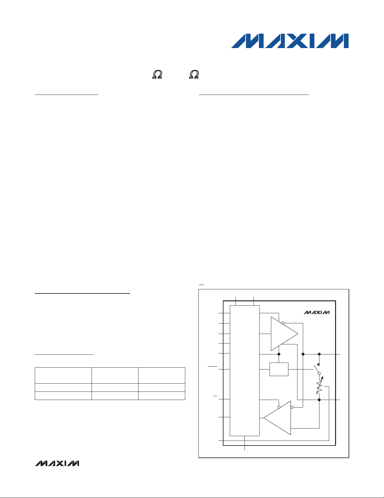
Functional Diagram (MAX13451E)
V
V
L
CC
SRL
INV
FAULT
TERM
DI
DE
LOGIC-LEVEL
TRANSLATION
RE
RO
D
LOGIC
MAX13451E
B
A
MAX13450E/MAX13451E
TERM100
GND
_______________________________________________________________ Maxim Integrated Products 1
For pricing, delivery, and ordering information, please contact Maxim Direct at 1-888-629-4642,
or visit Maxim’s website at www.maxim-ic.com.
RS-485 Transceivers with Integrated
100Ω/120Ω Termination Resistors
ABSOLUTE MAXIMUM RATINGS
(All voltages referenced to GND.)
VCC, VL ...................................................................-0.3V to +6V
DE, RE, DI, RO, TERM, TERM100, SRL ..... -0.3V to (VL + 0.3V)
INV, FAULT ................................................. -0.3V to (VL + 0.3V)
A, B, Z, Y ..................................................................-8V to +13V
A to B (High-Z State) ......................................................... +14V
B to A (High-Z State) ......................................................... +14V
Short-Circuit Duration (RO, Y, Z) to GND ................ Continuous
PACKAGE THERMAL CHARACTERISTICS (Note 1)
TSSOP
Junction-to-Ambient Thermal Resistance (qJA) ..........39°C/W
Junction-to-Case Thermal Resistance (qJC) .................3°C/W
Note 1: Package thermal resistances were obtained using the method described in JEDEC specification JESD51-7, using a four-
layer board. For detailed information on package thermal considerations, refer to www.maxim-ic.com/thermal-tutorial.
Stresses beyond those listed under “Absolute Maximum Ratings” may cause permanent damage to the device. These are stress ratings only, and functional
operation of the device at these or any other conditions beyond those indicated in the operational sections of the specifications is not implied. Exposure to absolute
maximum rating conditions for extended periods may affect device reliability.
MAX13450E/MAX13451E
ELECTRICAL CHARACTERISTICS
(VCC = +4.5V to +5.5V, VL = +1.62V to VCC, TA = T
VL = +1.8V, and TA = +25NC.) (Note 2)
PARAMETER SYMBOL CONDITIONS MIN TYP MAX UNITS
Supply Voltage V
Logic Supply Voltage V
Supply Current I
Logic Supply Current I
Shutdown Current I
DRIVER
Differential Driver Output V
Change in Magnitude of
Differential Output Voltage
Driver Common-Mode Output
Voltage
Change In Magnitude of
Common-Mode Voltage
Driver Short-Circuit Output
Current
CC
L
CC
L
SHDN
OD
DV
OD
V
OC
DV
OC
I
OSD
DE = RE = high, TERM = high, no load
DE = RE = low, TERM = low, no load
Current into VL, no load on RO, device not
switching, DE = RE = high
Current into VCC, DE = low, RE = TERM =
high
Current into VCC, DE = low, RE = high,
TERM = low
R
DIFF
R
DIFF
R
DIFF
R
DIFF
R
DIFF
0V P V
-7V P V
to T
MIN
= 100I, Figure 1 (Note 3)
= 46I, Figure 1 (Note 3)
= 100I or 46I, Figure 1 (Note 3)
= 100I or 46I, Figure 1 (Note 3)
= 100I or 46I, Figure 1 (Note 3)
P +12V
OUT
P 0V
OUT
Continuous Power Dissipation (TA = +70NC)
TSSOP (derate 25.6mW/NC above +70NC)................2051mW
Operating Temperature Range ....................... -40NC to +125NC
Storage Temperature Range .......................... -65NC to +150NC
Junction Temperature ....................................................+150NC
Lead Temperature (soldering, 10s) ...............................+300NC
Soldering Temperature (reflow) ......................................+260NC
unless otherwise noted. Typical values are at VCC = +5V,
MAX,
4.5 5.5 V
1.62 1.8 V
2.0 V
1.5 V
VCC/2 3 V
-250
CC
6
12
2
30
8 mA
CC
CC
0.2 V
0.2 V
+280
V
mA
FA
FA
V
mA
2 ______________________________________________________________________________________
RS-485 Transceivers with Integrated
100Ω/120Ω Termination Resistors
ELECTRICAL CHARACTERISTICS (continued)
(VCC = +4.5V to +5.5V, VL = +1.62V to VCC, TA = T
VL = +1.8V, and TA = +25NC.) (Note 2)
PARAMETER SYMBOL CONDITIONS MIN TYP MAX UNITS
Driver Short-Circuit Foldback
Output Current
RECEIVER
Input Current (A and B) I
Receiver Differential Threshold
Voltage
Receiver Input Hysteresis
LOGIC INTERFACE
Input High Voltage V
Input Low Voltage V
Input Current I
Receiver Output High Voltage V
Receiver Output Low Voltage V
Three-State Output Current at
Receiver
Receiver Output Short-Circuit
Current
Fault Output High Voltage
(MAX13451E)
Fault Output Low Voltage
(MAX13451E)
TERMINATION RESISTOR
100I Termination Resistor
120I Termination Resistor
Single-Ended Input Capacitance
vs. GND
ESD PROTECTION
ESD Protection (A, B, Y, Z)
ESD Protection (All Other Pins) Human Body Model
I
OSDF
A, B
V
TH
DV
IN
ROH
ROL
I
OZR
I
OSR
V
FAULTH
V
FAULTL
R
100
R
120
C
(VCC - 1V) P V
-7V P V
DE = RE = GND;
TERM = VL; VCC = GND
or 5.5V
-7V P VCM P +12V,
DE = RE = GND;
TERM = VL; VCC = GND
VA + VB = 0V 15 mV
TH
DI, DE, RE, TERM, SRL, TERM100, INV
IH
DI, DE, RE, TERM, SRL, TERM100, INV
IL
DI, DE, RE, TERM, TERM100, SRL, INV
I
OUT
I
OUT
0V P VRO P V
0V P VRO P V
Fault condition, I
Nonfault condition; I
TERM = low, TERM100 = high
TERM = low, TERM100 = low
f = 1MHz (MAX13451E only) 40 pF
IN
Human Body Model
IEC 61000-4-2 Contact Discharge
to T
MIN
OUT
= -1mA VL - 0.6 V
= +1mA 0.4 V
MAX,
OUT
P 0V
L
L
OUT
unless otherwise noted. Typical values are at VCC = +5V,
P +12V
VA or VB = +12V 125
VA or VB = -7V -100
VA or VB = +12V -200 -50 mV
= -1mA VL - 0.6 V
= +1mA 0.4 V
OUT
+15
2/3 x V
L
1/3 x V
-1 +1
-1 +0.01 +1
Q1 Q80
85 100 115
101 120 139
Q30
Q15
Q7
Q2
-15
L
MAX13450E/MAX13451E
mA
FA
V
V
FA
FA
mA
I
I
kVIEC 61000-4-2 Air Gap Discharge
_______________________________________________________________________________________ 3
RS-485 Transceivers with Integrated
100Ω/120Ω Termination Resistors
SWITCHING CHARACTERISTICS—SRL = HIGH
(VCC = +4.5V to +5.5V, VL = +1.62V to VCC, TA = T
VL = +1.8V and TA = +25NC.) (Note 2)
PARAMETER SYMBOL CONDITIONS MIN TYP MAX UNITS
DRIVER
t
Driver Propagation Delay
Differential Driver Output Skew
|t
- t
DPLH
Driver Differential Output Rise or
Fall Time
Maximum Data Rate DR
Driver Enable from Shutdown to
Output High
Driver Enable from Shutdown to
Output Low
Driver Disable Delay t
Driver Enable Delay t
RECEIVER
MAX13450E/MAX13451E
Receiver Propagation Delay
Receiver Output Skew t
Maximum Data Rate DR
Receiver Enable to Output High t
Receiver Enable to Output Low t
Receiver Disable from High t
Receiver Disable from Low t
Receiver Enable from Shutdown
to Output High
Receiver Enable from Shutdown
to Output Low
TERMINATION RESISTOR
Turn-Off Time t
Turn-On Time t
DPHL
|
DPLH
t
DPHL
t
DSKEW
t
HL
t
LH
MAX
t
DZH(SHDN)
t
DZL(SHDN)
, t
DLZ
DHZ
, t
DZL
DZH
t
RPLH
t
RPHL
RSKEW
MAX
RZH
RZL
RHZ
RLZ
t
RZH(SHDN)
t
RZL(SHDN)
RTZ
RTEN
R
DIFF
R
DIFF
R
DIFF
S2 closed, RL = 500I, CL = 100pF,
Figures 4 and 5
S1 closed, RL = 500I, CL = 100pF,
Figures 4 and 5
Figures 4 and 5 100 ns
Figures 4 and 5 2500 ns
CL = 15pF, |VID| R 2.0V; tLH, tHL P 15ns,
Figures 6 and 7
CL = 15pF, Figures 6 and 7 30 ns
S2 closed, CL = 100pF, RL = 500I,
Figures 8 and 9
S1 closed, CL = 100pF, RL = 500I,
Figures 8 and 9
Figures 8 and 9 50 ns
Figures 8 and 9 50 ns
Figures 8 and 9 5000 ns
Figures 8 and 9 5000 ns
Figure 10 120
Figure 10 1
to T
MIN
= 54I, CL = 50pF, Figures 2 and 3
= 54I, CL = 50pF, Figure 3
= 54I, CL = 50pF, Figures 2 and 3
unless otherwise noted. Typical values are at VCC = +5V,
MAX,
800
800
100 ns
100 600
100 600
500 kbps
4500 ns
5200 ns
200
200
500 kbps
50 ns
50 ns
ns
ns
ns
Fs
Fs
4 ______________________________________________________________________________________
RS-485 Transceivers with Integrated
100Ω/120Ω Termination Resistors
SWITCHING CHARACTERISTICS—SRL = LOW
(VCC = +4.5V to +5.5V, VL = +1.62V to VCC, TA = T
VL = +1.8V, and TA = +25NC.) (Note 2)
PARAMETER SYMBOL CONDITIONS MIN TYP MAX UNITS
DRIVER
t
Driver Propagation Delay
Differential Driver Output Skew
|t
- t
DPLH
Driver Differential Output Rise or
Fall Time
Maximum Data Rate DR
Driver Enable from Shutdown to
Output High
Driver Enable from Shutdown to
Output Low
Driver Disable Delay t
Driver Enable Delay t
RECEIVER
Receiver Propagation Delay
Receiver Output Skew t
Maximum Data Rate DR
Receiver Enable to Output High t
Receiver Enable to Output Low t
Receiver Disable Time from High t
Receiver Disable Time from Low t
Receiver Enable from Shutdown
to Output High
Receiver Enable from Shutdown
to Output Low
TERMINATION RESISTOR
Turn-Off Time t
Turn-On Time t
Note 2: All devices are 100% production tested at TA = +25°C. Limits over temperature are guaranteed by design.
Note 3: Termination resistance is disabled (TERM = high).
DPHL
|
DPLH
t
DPHL
t
DSKEW
tHL, t
LH
MAX
t
DZH(SHDN)
t
DZL(SHDN)
, t
DLZ
DHZ
, t
DZL
DZH
t
RPLH
t
RPHL
RSKEW
MAX
RZH
RZL
RHZ
RLZ
t
RZH(SHDN)
t
RZL(SHDN)
RTZ
RTEN
R
DIFF
R
DIFF
R
DIFF
S2 closed, RL = 500I, CL = 100pF,
Figures 4 and 5
S1 closed, RL = 500I, CL = 100pF,
Figures 4 and 5
Figures 4 and 5 100 ns
Figures 4 and 5 100 ns
CL = 15pF, |VID| R 2.0V; tLH, tHL P 15ns,
Figures 6 and 7
CL = 15pF, Figures 6 and 7 6 ns
S2 closed, CL = 100pF, RL = 500I,
Figures 8 and 9
S1 closed, CL = 100pF, RL = 500I,
Figures 8 and 9
Figures 8 and 9 50 ns
Figures 8 and 9 50 ns
Figures 8 and 9 2000 ns
Figures 8 and 9 2000 ns
Figure 10 120
Figure 10 1
to T
MIN
= 54I, CL = 50pF, Figures 2 and 3
= 54I, CL = 50pF, Figure 3
= 54I, CL = 50pF, Figures 2 and 3
unless otherwise noted. Typical values are at VCC = +5V,
MAX,
20 Mbps
20 Mbps
50
50
6 ns
15 ns
2000 ns
2000 ns
50
50
50 ns
50 ns
ns
ns
Fs
Fs
MAX13450E/MAX13451E
_______________________________________________________________________________________ 5
RS-485 Transceivers with Integrated
100Ω/120Ω Termination Resistors
Typical Operating Characteristics
(VCC = +5V, VL = +1.8V, TA = +25NC, unless otherwise noted.)
SUPPLY CURRENT
vs. DATA RATE
70
60
RL = 54Ω
50
RL = 100Ω
40
30
SUPPLY CURRENT (mA)
20
10
NO LOAD
0
0.1 100
DATA RATE (Mbps)
101
10
9
8
MAX13450E/51E toc01
7
6
5
4
3
SHUTDOWN CURRENT (µA)
2
1
0
-40 125
RECEIVER OUTPUT HIGH VOLTAGE
vs. TEMPERATURE
2.0
MAX13450E/MAX13451E
I
= 1mA
OUT
1.8
1.6
1.4
0.5
0.4
MAX13450E/51E toc04
0.3
0.2
SHUTDOWN CURRENT
vs. TEMPERATURE
RECEIVER OUTPUT LOW VOLTAGE
vs. TEMPERATURE
I
= 1mA
OUT
TEMPERATURE (°C)
1109565 80-10 5 20 35 50-25
5
SOURCE
MAX13450E/51E toc02
4
3
2
RECEIVER OUTPUT VOLTAGE (V)
1
SINK
0
0 70
RECEIVER PROPAGATION DELAY
100
INV = HIGH
80
MAX13450E/51E toc05
60
40
RECEIVER OUTPUT VOLTAGE
vs. OUTPUT CURRENT
MAX13450E/51E toc03
605040302010
OUTPUT CURRENT (mA)
vs. TEMPERATURE
MAX13450E/51E toc06
INV = LOW
1.2
RECEIVER OUTPUT HIGH VOLTAGE (V)
1.0
-40 125
TEMPERATURE (°C)
DRIVER DIFFERENTIAL OUTPUT CURRENT
vs. DIFFERENTIAL OUTPUT VOLTAGE
100
80
60
40
20
DRIVER DIFFERENTIAL OUTPUT CURRENT (mA)
0
0 5
DRIVER DIFFERENTIAL OUTPUT VOLTAGE (V)
0.1
RECEIVER OUTPUT LOW VOLTAGE (V)
0
1109580655035205-10-25
-40 125
TEMPERATURE (°C)
1109580655035205-10-25
TRANSMITTER OUTPUT CURRENT
vs. TRANSMITTER OUTPUT HIGH VOLTAGE
120
100
MAX13450E/51E toc07
80
60
40
20
TRANSMITTER OUTPUT CURRENT (mA)
0
4321
-7
TRANSMITTER OUTPUT HIGH VOLTAGE (V)
3-2
20
RECEIVER PROPAGATION DELAY (ns)
0
-40 125
TRANSMITTER OUTPUT CURRENT
vs. TRANSMITTER OUTPUT LOW VOLTAGE
200
180
160
MAX13450E/51E toc08
140
120
100
80
60
40
TRANSMITTER OUTPUT CURRENT (mA)
20
0
-3 12
TRANSMITTER OUTPUT LOW VOLTAGE (V)
TEMPERATURE (°C)
6 ______________________________________________________________________________________
1109580655035205-10-25
MAX13450E/51E toc09
72

RS-485 Transceivers with Integrated
100Ω/120Ω Termination Resistors
Typical Operating Characteristics (continued)
(VCC = +5V, VL = +1.8V, TA = +25NC, unless otherwise noted.)
MAX13450E/MAX13451E
DRIVER DIFFERENTIAL OUTPUT VOLTAGE
vs. TEMPERATURE
5
R
= 54Ω
DIFF
4
3
2
1
DRIVER DIFFERENTIAL OUTPUT VOLTAGE (V)
0
-40 125
TEMPERATURE (°C)
120Ω TERMINATION RESISTOR
vs. FREQUENCY
140
120
100
R
MAGNITUDE
120
80
60
MAGNITUDE (Ω)
40
20
R
120
PHASE
1109580655035205-10-25
MAX13450E/51E toc12
MAX13450E/51E toc10
0
PHASE (DEGREE)
-10
-20
100Ω TERMINATION RESISTOR
vs. FREQUENCY
140
120
100
80
R
MAGNITUDE
100
60
MAGNITUDE (Ω)
40
20
0
0.1 100
R
100
FREQUENCY (MHz)
PHASE
101
TERMINATION RESISTANCE
vs. TEMPERATURE
130
120
120Ω RESISTOR
110
100
100Ω RESISTOR
TERMINATION RESISTANCE (Ω)
90
MAX13450E/51E toc11
0
PHASE (DEGREE)
-10
-20
-30
MAX13450E/51E toc13
0
0.1 100
FREQUENCY (MHz)
101
DRIVER PROPAGATION DELAY (250kbps)
(MAX13451E)
SRL = HIGH
DE = HIGH
RE = HIGH
1µs/div
MAX13450E/51E toc14
-30
DI
1V/div
A
1V/div
B
1V/div
80
-40 125
TEMPERATURE (°C)
DRIVER ENABLE TIME FROM SHUTDOWN
(MAX13451E)
200ns/div
MAX13450E/51E toc15
SRL = LOW
RE = HIGH
1109580655035205-10-25
DE
2V/div
A
2V/div
B
2V/div
_______________________________________________________________________________________ 7

RS-485 Transceivers with Integrated
100Ω/120Ω Termination Resistors
Test Circuits and Waveforms
A/Y
R
DIFF
2
V
OD
B/Z
C
L
R
DIFF
2
V
OC
Figure 1. Driver DC Test Load
V
L
DI
MAX13450E/MAX13451E
0V
B
A
1/2 V
V
O
V
O
V
0V
DD
-V
O
10%
t
LH
VL/2
O
f = 1MHz, tLH ≤ 3ns, tHL ≤ 3ns
t
DPLH
90%
t
V
L
DE
DI
Figure 2. Driver Timing Test Circuit
/2
V
L
t
DPHL
90%
t
HL
= |t
- t
DSKEW
DPLH
DPHL
|
A
V
ID
B
10%
1/2 V
R
DIFF
O
C
L
Figure 3. Driver Propagation Delays
8 ______________________________________________________________________________________
RS-485 Transceivers with Integrated
100Ω/120Ω Termination Resistors
Test Circuits and Waveforms (continued)
V
L
DE
0V
V
CC
A/Y, B/Z
V
OL
V
OH
A/Y, B/Z
0V
Figure 4. Driver Enable and Disable Times
Ω
OUTPUT
UNDER TEST
500
C
L
VL/2
t
DZL(SHDN),tDZL
(VCC + VOL)/2
V
/2
OH
V
S1
S2
CC
OUTPUT NORMALLY LOW
OUTPUT NORMALLY HIGH
t
DZH(SHDN),tDZH
ATE
t
t
DLZ
DHZ
V
/2
L
+ 0.25V
V
OL
- 0.25V
V
OH
B
V
ID
R
A
RECEIVER
OUTPUT
MAX13450E/MAX13451E
Figure 5. Driver-Enable and Disable-Timing Test Load
A
B
V
ROH
RO
V
ROL
Figure 7. Receiver Propagation Delays
_______________________________________________________________________________________ 9
VL/2
f = 1MHz, t
t
RPHL
Figure 6. Receiver Propagation Delay Test Circuit
≤ 3ns, tHL ≤ 3ns
LH
t
RPLH
V
/2
L
t
= |t
- t
RSKEW
RPHL
RPLH
|
1V
-1V

RS-485 Transceivers with Integrated
100Ω/120Ω Termination Resistors
Test Circuits and Waveforms (continued)
V
L
RE
RO
RO
0V
V
V
ROL
V
ROH
0V
DI = 0V
L
VL/2
t
RZL(SHDN)
(VL + V
V
/2
ROH
t
RZH(SHDN)
, t
RZL
)/2
ROL
OUTPUT NORMALLY LOW
OUTPUT NORMALLY HIGH
, t
RZH
Figure 8. Receiver Enable and Disable Times
MAX13450E/MAX13451E
500
RO
Ω
C
L
S1
S2
V
/2
L
t
RHZ
R
+ 0.25V
OH
R
- 0.25V
OH
t
RHZ
V
CC
Figure 9. Receiver Enable and Disable Times
= VAB/R
I
A
TERM
D
A
RECEIVERRO
B
TERM
V
L
VL/2
0V
I
A
90%
V
RD = R
= VA - V
AB
t
REN
B
OR R
100
200
Figure 10. Termination Resistor Turn-On/-Off Times
10 _____________________________________________________________________________________
10%
t
REN

RS-485 Transceivers with Integrated
100Ω/120Ω Termination Resistors
Pin Configurations
MAX13450E/MAX13451E
TOP VIEW
CC
L
+
MAX13450E
*EP
TSSOP
141 SRLDE
132 TERM100RE
123 ZDI
114 GNDV
105 YTERM
96 BV
87 ARO
*CONNECT EP TO GND
TOP VIEW
CC
L
+
MAX13451E
*EP
TSSOP
141 SRLDE
132 TERM100RE
123 BDI
114 GNDV
105 ATERM
96 FAULTV
87 INVRO
Pin Description
PIN
MAX13450E MAX13451E
1 1 DE
2 2
3 3 DI
4 4 V
5 5
6 6 V
7 — RO
— 7 RO
8 — A Noninverting Receiver Input
— 10 A
9 — B Inverting Receiver Input
— 12 B
NAME FUNCTION
Driver-Output Enable. Drive DE low to put the driver output in three-state. Drive DE
high to enable the driver. DE is referenced to VL.
Receiver-Output Enable. Drive RE low to enable the RO. Drive RE high to disable
RE
the RO output and put the RO output in a high-impedance state. RE is referenced
to VL.
Driver Input. Drive DI low to force the noninverting output low and the inverting
output high. Drive DI high to force the noninverting output high and inverting output low. DI is referenced to VL.
CC
TERM
L
Power-Supply Voltage. Bypass VCC to GND with a 0.1FF ceramic capacitor
placed as close as possible to the device.
Active-Low Termination Resistor Enable. Drive TERM low to enable the internal termination resistor. TERM is referenced to VL.
Logic Supply Voltage. Bypass VL to GND with a 0.1FF ceramic capacitor placed
as close as possible to the device.
Receiver Output. When receiver is enabled and VA - VB R -50mV, RO is high. If
VA - VB P -200mV, RO is low. RO is referenced to VL.
Receiver Output. When INV is low, receiver is enabled and VA - VB R -50mV, RO is
high. If VA - VB P -200mV, RO is low. When INV is high, receiver is enabled and
VA - VB R -50mV, RO is low. If VA - VB P -200mV, RO is high. RO is referenced to VL.
If INV is low, A is a noninverting receiver input and a noninverting driver output. If
INV is high, A is an inverting receiver input and an inverting driver output.
If INV is low, B is an inverting receiver input and an inverting driver output. If INV
is high, B is a noninverting receiver input and a noninverting driver output.
______________________________________________________________________________________ 11

RS-485 Transceivers with Integrated
100Ω/120Ω Termination Resistors
Pin Description (continued)
PIN
MAX13450E MAX13451E
10 — Y Noninverting Driver Output
11 11 GND Ground
12 — Z Inverting Driver Output
13 13 TERM100
14 14 SRL
— 8 INV
— 9 FAULT
— — EP Exposed Pad. Connect EP to GND. Do not use EP as the only GND connection.
Function Tables
MAX13450E/MAX13451E
Table 1. Termination Resistor Control
(MAX13450E/MAX13451E)
TERM
Low X X Activated
High X X Not activated
DE
RE
Table 2. Shutdown Control (MAX13450E/
NAME FUNCTION
Termination Resistor Value Selection Input. Drive TERM100 low to select a 120I
termination and high to select a 100I termination. The TERM100 input is referenced to VL.
Slew-Rate Limiting-Enable Input. Drive SRL high to enable slew-rate limiting and
low to disable slew-rate limiting. The SRL input is referenced to VL.
Inversion Input. Drive INV high to internally swap RO logic level with respect to A
and B signals.
Fault Flag Output. FAULT asserts high in overcurrent conditions or if A/B are forced
below GND or above VCC when the driver is enabled. FAULT is referenced to VL.
Table 4. Function Table for Receiver
(MAX13450E)
TERMINATION RESISTOR
RE
High X High-Z
Low
INPUT OUTPUT
A-B RO
R -50mV or Open
P -200mV
High
Low
MAX13451E)
DE
Low High High Shutdown
RE TERM
Table 3. Function Table for Transmitter
(MAX13450E)
INPUT OUTPUT
DE DI Y Z
Low X High-Z High-Z
High
12 _____________________________________________________________________________________
Low Low High
High High Low
STATE
Table 5. INV Input Function Table for
Transmitter (MAX13451E)
INPUT OUTPUT
DE INV DI A B
Low X X High-Z High-Z
Low
High
High
Low Low High
High High Low
Low High Low
High Low High

RS-485 Transceivers with Integrated
100Ω/120Ω Termination Resistors
Function Tables
(continued)
Table 6. INV Input Function Table for
Receiver (MAX13451E)
INPUT OUTPUT
RE
High X X High-Z
Low
INV A-B RO
Low
High
R -50mV or
Short or Open
P -200mV
R -50mV or
Open
P -200mV
High
Low
Low
High
Functional Diagram (MAX13450E)
V
V
L
CC
SRL
Z
DI
DE
TERM
LOGIC-LEVEL
TRANSLATION
RE
D
Y
MAX13450E
B
MAX13450E/MAX13451E
Detailed Description
The MAX13450E is a full-duplex, RS-485/RS-422compatible transceiver and the MAX13451E is a halfduplex, RS-485/RS-422-compatible transceiver. Both
devices have an internal 100I/120I termination resistor.
The MAX13450E/MAX13451E have a VL supply voltage
input to support down to a +1.8V voltage logic interface.
The MAX13450E/MAX13451E feature a 1/8-unit load
receiver input impedance, allowing up to 256 transceivers on the bus. All line interface pins are protected to
Q30kV ESD based on the HBM. These devices also
include fail-safe circuitry, guaranteeing a defined logiclevel receiver output when the receiver inputs are open
or shorted.
The MAX13450E/MAX13451E allow slew-rate-limited
driver outputs for lower data rates below 500kbps. The
SRL reduces the slew rate, which reduces EMI emissions
and reflections caused by improperly terminated cables.
The MAX13451E has a FAULT output that indicates a
fault condition on the driver. The MAX13451E also has an
INV input that inverts the phase of A and B pins.
Termination Resistor
The MAX13450E/MAX13451E feature a selectable inter-
nal termination resistor. Drive the TERM input low to
enable the internal termination resistor. Drive the TERM
input high to disable the internal termination resistor.
RO
A
TERM100
GND
Drive the TERM100 input high to select the 100I termination resistor. Drive TERM100 input low to select the
120I termination resistor.
INV Input (MAX13451E)
The INV input of the MAX13451E reverses the polarity
of the RO receiver output (see Table 5 and 6). If the INV
input is high then the RO output is low under fail-safe
receiver conditions. This is the opposite polarity of normal fail-safe operations.
Fault Condition (MAX13451E)
The MAX13451E also has a FAULT output to indicate a
fault condition. The FAULT output is active high when
there is a short circuit at the driver’s output, an over/
undervoltage at the driver’s outputs, or the device’s temperature is higher than +150NC.
______________________________________________________________________________________ 13

RS-485 Transceivers with Integrated
100Ω/120Ω Termination Resistors
Thermal Shutdown
When the devices’ temperature goes over +150NC, the
termination resistor turns off, and the transmitter shuts
down while the receiver stays active.
Fail Safe
The MAX13450E guarantee a logic-high receiver output
when the receiver inputs are shorted or open, or when
they are connected to a terminated transmission line with
all drivers disabled. This is done by setting the receiver
input threshold between -50mV and -200mV. If the differential receiver input voltage (A - B) is greater than
or equal to -50mV, RO is logic-high. If (A - B) is less
than or equal to -200mV, RO is logic-low. In the case
of a terminated bus with all transmitters disabled, the
receiver’s differential input voltage is pulled to 0V by the
termination resistor. With the receiver thresholds of the
MAX13450E, this results in RO being logic-high.
The MAX13451E has the same fail-safe receiver behavior
as the MAX13450E when the INV input is low. When the
INV input is high, RO is low under the fail-safe condition.
MAX13450E/MAX13451E
As with all Maxim devices, ESD-protection structures
are incorporated on all pins to protect against electrostatic discharges encountered during handling and
assembly. The driver outputs and receiver inputs of the
MAX13450E/MAX13451E have extra protection against
static electricity. The ESD structures withstand high ESD
in all states: normal operation, shutdown, and powered
down. After an ESD event, the MAX13450E/MAX13451E
keep working without latchup or damage.
ESD protection can be tested in various ways. The transmitter outputs and receiver inputs of the MAX13450E/
MAX13451E are characterized for protection to the following limits:
• Q30kV using the Human Body Model
• Q15kV using the Air Gap Discharge Method specified
in IEC 61000-4-2
• Q7kV using the Contact Discharge Method specified
in IEC 61000-4-2
ESD performance depends on a variety of conditions.
Contact Maxim for a reliability report that documents test
setup, test methodology, and test results.
ESD Protection
ESD Test Conditions
Human Body Model
Figure 11a shows the Human Body Model, and Figure
11b shows the current waveform it generates when discharged into a low impedance. This model consists of a
100pF capacitor charged to the ESD voltage of interest,
which is then discharged into the test device through a
1.5kI resistor.
IEC 61000-4-2
The IEC 61000-4-2 standard covers ESD testing and
performance of finished equipment. However, it does not
specifically refer to integrated circuits. The MAX13450E/
MAX13451E help equipment designs to meet IEC 610004-2, without the need for additional ESD-protection
components. The major difference between tests done
using the Human Body Model and IEC 61000-4-2 is
higher peak current in IEC 61000-4-2 because series
resistance is lower in the IEC 61000-4-2 model. Hence,
the ESD withstand voltage measured to IEC 61000-4-2
is generally lower than that measured using the Human
Body Model. Figure 11c shows the IEC 61000-4-2 model,
and Figure 11d shows the current waveform for the IEC
61000-4-2 ESD Contact Discharge test.
Applications Information
Typical Applications
The MAX13450E transceiver is designed for full-duplex,
bidirectional data communications on point-to-point
or multipoint bus transmission lines (Figure 12). The
MAX13451E transceiver is designed for half-duplex,
bidirectional data communications on point-to-point or
multipoint bus transmission lines (Figure 13).
256 Transceivers on the Bus
The standard RS-485 receiver input impedance is oneunit load, and the standard driver can drive up to 32-unit
loads. The MAX13450E/MAX13451E have a 1/8-unit load
receiver input impedance, allowing up to 256 transceivers to be connected in parallel on one communication
line. Any combination of these devices, as well as other
RS-485 transceivers with a total of 32-unit loads or fewer,
can be connected to the line.
Reduced EMI and Reflections
The MAX13450E/MAX13451E feature reduced slew-rate
drivers that minimize EMI and reduce reflections caused
by improperly terminated cables, allowing error-free data
transmission up to 500kbps.
14 _____________________________________________________________________________________

1M
RS-485 Transceivers with Integrated
100Ω/120Ω Termination Resistors
MAX13450E/MAX13451E
R
C
Ω
RD
1500
R
Ω
C
50MΩ TO 100MΩ
R
330Ω
D
DISCHARGE
RESISTANCE
STORAGE
C
S
CAPACITOR
HIGH-
VOLTAGE
DC
SOURCE
CHARGE-CURRENT
LIMIT RESISTOR
100pF
Figure 11a. Human Body ESD Test Model
I
r
t
DL
PEAK-TO-PEAK RINGING
(NOT DRAWN TO SCALE)
AMPS
IP 100%
90%
36.8%
10%
0
0
t
RL
TIME
CURRENT WAVEFORM
Figure 11b. Human Body Current Waveform
DEVICE
UNDER
TEST
DISCHARGE
RESISTANCE
STORAGE
C
S
CAPACITOR
DEVICE
UNDER
TEST
HIGH-
VOLTAGE
DC
SOURCE
CHARGE-CURRENT
LIMIT RESISTOR
150pF
Figure 11c. IEC 61000-4-2 ESD Test Model
I
100%
90%
PEAK
I
10%
tr = 0.7ns TO 1ns
30ns
60ns
t
Figure 11d. IEC 61000-4-2 ESD Generator Current Waveform
Typical Application Circuits
Z
D
Y
B
R
A
MAX13450E
MASTER END SLAVE
R
D
SLAVE 1
Figure 12. Full-Duplex, Multidrop (MAX13450E)
______________________________________________________________________________________ 15
D
SLAVE 2
R
D
SLAVE N
R
B
R
A
Z
D
Y
MAX13450E
RS-485 Transceivers with Integrated
100Ω/120Ω Termination Resistors
Typical Application Circuits (continued)
MAX13451E MAX13451E
D
R
MAX13450E/MAX13451E
Figure 13. Half-Duplex, Multidrop, and Point-to-Point Systems (MAX13451E)
B
A
R
D
SLAVE 1
D
SLAVE 2
Low-Power Shutdown Mode
Drive RE high, DE low, and TERM high to enter lowpower shutdown mode (see Table 2).
Chip Information
PROCESS: BiCMOS
B
A
R
D
R
SLAVE N
D
R
Package Information
For the latest package outline information and land patterns,
go to www.maxim-ic.com/packages. Note that a “+”, “#”, or
“-” in the package code indicates RoHS status only. Package
drawings may show a different suffix character, but the drawing
pertains to the package regardless of RoHS status.
PACKAGE
TYPE
14 TSSOP-EP U14E+3
PACKAGE
CODE
OUTLINE
NO.
21-0108 90-0119
LAND
PATTERN NO.
16 _____________________________________________________________________________________

RS-485 Transceivers with Integrated
100Ω/120Ω Termination Resistors
Revision History
MAX13450E/MAX13451E
REVISION
NUMBER
0 4/10 Initial release —
1 11/10
REVISION
DATE
DESCRIPTION
Updated the VL specification in the Electrical Characteristics and Switching
Characteristics tables
PAGES
CHANGED
2–5
Maxim cannot assume responsibility for use of any circuitry other than circuitry entirely embodied in a Maxim product. No circuit patent licenses are implied.
Maxim reserves the right to change the circuitry and specifications without notice at any time.
Maxim Integrated Products, 120 San Gabriel Drive, Sunnyvale, CA 94086 408-737-7600 17
©
2010 Maxim Integrated Products Maxim is a registered trademark of Maxim Integrated Products, Inc.
 Loading...