

Page 1
General Description
The MAX13448E full-duplex RS-485 transceiver features inputs and outputs fault protected up to ±80V
(with respect to ground). The device operates from a
+3.0V to +5.5V supply and features true fail-safe circuitry, guaranteeing a logic-high receiver output when
the receiver inputs are open or shorted. This enables all
receiver outputs on a terminated bus to output logichigh when all transmitters are disabled.
The MAX13448E features a slew-rate limited driver that
minimizes EMI and reduces reflections caused by
improperly terminated cables, allowing error-free data
transmission at data rates up to 500kbps with a +5V
supply, and 250kbps with a +3.3V supply.
The MAX13448E includes a hot-swap capability to eliminate false transitions on the bus during power-up or hot
insertion. The driver and receiver feature active-high and
active-low enables, respectively, that can be connected
together externally to serve as a direction control.
The MAX13448E features an 1/8-unit load receiver input
impedance, allowing up to 256 transceivers on the bus.
All driver outputs are protected to ±8kV ESD using the
Human Body Model. The MAX13448E is available in a
14-pin SO package and operates over the extended
-40°C to +85°C temperature range.
Applications
Industrial Control Systems
HVAC Control systems
Utility Meters
Motor Driver Control Systems
Features
o ±80V Fault Protection on the RS-485 I/O Ports
o True Fail-Safe Receiver
o Hot-Swap Input Structure on DE
o ESD Protection on the RS-485 I/O Ports
±8kV Human Body Model
o Slew-Rate Limiting Facilitates Error-Free Data
Transmission
o 1/8-Unit Load Allows Up to 256 Transceivers on
the Bus
o -7V to +12V Common-Mode Input Voltage Range
o +3.0V to +5.5V Operating Supply Voltage
o Available in 14-Pin SO Package
MAX13448E
±80V Fault-Protected Full-Duplex
RS-485 Transceiver
________________________________________________________________
Maxim Integrated Products
1
Ordering Information
19-4098; Rev 0; 5/08
For pricing, delivery, and ordering information, please contact Maxim Direct at 1-888-629-4642,
or visit Maxim’s website at www.maxim-ic.com.
Pin Configuration appears at end of data sheet.
+
Denotes a lead-free package.
R
t
RE
RO
Y
Z
DI
9
10
A
B
R
t
12
11
6, 73
R
D
R
DI
D
DE
RE
RO
N.C.
R
D
DE
GND
GND
V
CC
1μF
141
SO
+
V
CC
N.C.
132 N.C.RO
123ARE
114BDE
105ZDI
96YGND
87 N.C.GND
1, 8,
13
2
5
414
V
CC
MAX13448E
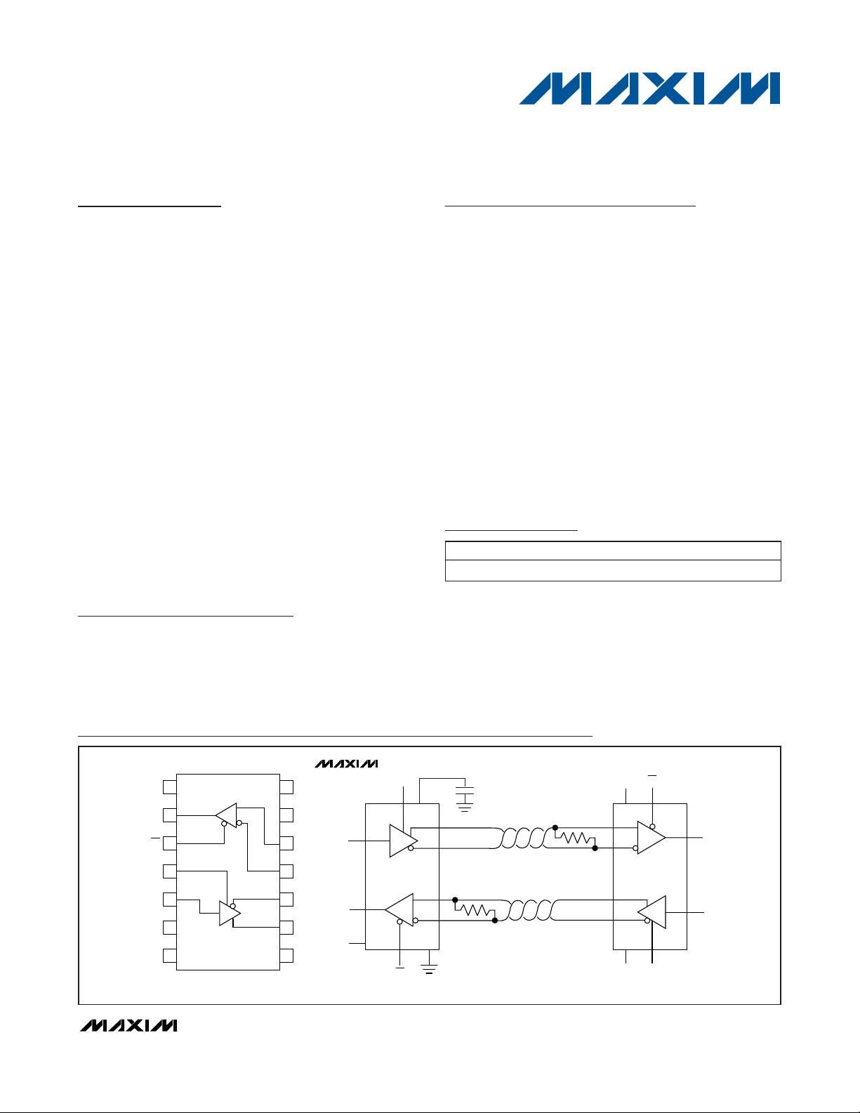
Functional Diagram
PART TEMP RANGE PIN-PACKAGE
MAX13448EESD+ -40°C to +85°C 14 SO
Page 2
MAX13448E
±80V Fault-Protected Full-Duplex
RS-485 Transceiver
2 _______________________________________________________________________________________
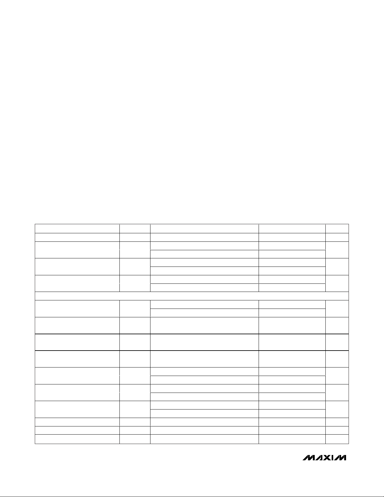
ABSOLUTE MAXIMUM RATINGS
ELECTRICAL CHARACTERISTICS
(VCC= +3.0 to +5.5V, TA= T
MIN
to T
MAX
, unless otherwise noted. Typical values are at VCC= +3.3V and TA= +25°C.) (Notes 2, 3)
Stresses beyond those listed under “Absolute Maximum Ratings” may cause permanent damage to the device. These are stress ratings only, and functional
operation of the device at these or any other conditions beyond those indicated in the operational sections of the specifications is not implied. Exposure to
absolute maximum rating conditions for extended periods may affect device reliability.
(All voltages reference to GND.)
Supply Voltage (V
CC
).............................................................+6V
Control Input Voltage (RE, DE)...................-0.3V to (V
CC
+ 0.3V)
Driver Input Voltage (DI).............................-0.3V to (V
CC
+ 0.3V)
Receiver Input Voltage (A, B (Note 1)) ................................±80V
Driver Output Voltage (Y, Z (Note 1)) ..................................±80V
Receiver Output Voltage (RO)....................-0.3V to (V
CC
+ 0.3V)
Short-Circuit Duration (RO, A, B) ...............................Continuous
Continuous Power Dissipation (T
A
= +70°C)
14-Pin SO (derate 8.3mW/°C above +70°C)................667mW
Operating Temperature Range ...........................-40°C to +85°C
Junction Temperature......................................................+150°C
Storage Temperature Range .............................-65°C to +150°C
Lead Temperature (soldering, 10s) .................................+300°C
Note 1: If the RS-485 transmission lines are unterminated and a short to a voltage V
SHT
occurs at a remote point on the line, an active
local driver (with DI switching) may see higher voltage than V
SHT
due to inductive kickback at the driver. Terminating the line
with a resistor equal to its characteristic impedance minimizes this kickback effect.
PARAMETER SYMBOL CONDITION MIN TYP MAX UNITS
VCC Supply Voltage Range V
Supply Current I
Supply Current in Shutdown
Mode
Supply Current with Output
Shorted to ±60V
DRIVER
Differential Driver Output V
Change in Magnitude of
Differential Output Voltage
Driver Common-Mode Output
Voltage
Change in Magnitude of
Common-Mode Voltage
Driver Short-Circuit Output
Current
Driver Short-Circuit Foldback
Output Current
Driver-Limit Short-Circuit
Foldback Output Current
Driver Input High Voltage V
Driver Input Low Voltage V
Driver Input Current I
CC
I
SHDN
I
SHRT
OD
ΔV
V
OC
ΔV
I
OSD
I
OSDF
I
OSDL
DIH
DIL
DIN
N o l oad , D E , D I, RE = 0V or V
Q
No load, DE, DI, RE = 0V or VCC, VCC = 5V 15
DE = GND, RE = VCC, VCC = 3.3V 100
DE = GND, RE = VCC, VCC = 5V 100
DE = GND, RE = GND, short to +60V 15
DE = GND, RE = GND, short to -60V 15
RL = 100Ω, Figure 1 2 V
RL = 54Ω, Figure 1 1.5 V
RL = 100Ω or 54Ω, Figure 1 (Note 4) -0.2 0.2 V
OD
RL = 100Ω or 54Ω, Figure 1 VCC/2 3 V
RL = 100Ω or 54Ω, Figure 1 (Note 4) -0.2 +0.2 V
OC
DI = low, 0V ≤ VY or VZ ≤ +12V +250
DI = high, -7V ≤ VY or VZ ≤ VCC (Note 5) -250
DI = low, (VCC - 1V) ≤ VY or VZ ≤ +12V +10
DI = high, -7V ≤ VY or VZ ≤ +1V -10
VY or VZ ≥ + 22V, RL = 100Ω +6
VY or VZ ≤ -13V, RL = 100Ω -6
2V
0.8 V
-1 +1 µA
, V
= 3.3V 15
C C
C C
3.0 5.5 V
CC
CC
mA
µA
mA
V
mA
mA
mA
Page 3
MAX13448E
±80V Fault-Protected Full-Duplex
RS-485 Transceiver
_______________________________________________________________________________________ 3
ELECTRICAL CHARACTERISTICS (continued)
(VCC= +3.0 to +5.5V, TA= T
MIN
to T
MAX
, unless otherwise noted. Typical values are at VCC= +3.3V and TA= +25°C.) (Notes 2, 3)
SWITCHING CHARACTERISTICS (VCC= +3.3V ±10%)
(TA= T
MIN
to T
MAX
, unless otherwise noted. Typical values are at VCC= +3.3V and TA= +25°C.)
PARAMETER SYMBOL CONDITION MIN TYP MAX UNITS
RECEIVER
Input Current IA,
Receiver Differential Threshold
Voltage
Receiver Input Hysteresis ΔV
Output High Voltage V
Output Low Voltage V
Three-State Output Current at
Receiver
Receiver Output Short-Circuit
Current
ESD PROTECTION
All Pins Human Body Model ±2 kV
ESD Protection Level
(A and B, Y and Z)
CONTROL
Control Input High Voltage V
Control Input Low Voltage V
Input Current Latch During First
Rising Edge
PROTECTION SPECIFICATIONS
Overvoltage Protection A, B, Y, Z -80 +80 V
V
= GND or
CC
= +3.0V to +5.5V
V
CC
25 mV
V
-
CC
0.6
-1 +1 µA
-95 +95 mA
V
I
OZR
I
OSR
I
TH
TH
OH
OL
CIH
CIL
IN
VA, VB = +12V
B
VA, VB = -7V -100 µA
VA, VB = ±80V -6 +6 mA
-7V ≤ V
IOH = -1.6mA
IOL = 1mA 0.4 V
0 ≤ VA, VB ≤ V
0 ≤ VRO ≤ V
Human Body Model ±8 kV
DE, RE 2V
DE, RE 0.8 V
DE, RE 80 µA
≤ +12V -200 -50 mV
CM
CC
CC
+125 µA
V
DRIVER
Driver Differential Propagation
Delay
Driver Differential Output
Transition Time
Differential Driver Output Skew t
Maximum Data Rate f
D r i ver E nab l e Ti m e to Outp ut H i g ht
PARAMETER SYMBOL CONDITION MIN TYP MAX UNITS
t
,
DPLH
t
DPHL
, t
t
LH
DSKEW
MAX
DZH
RL = 54Ω, CL = 50pF, Figures 2 and 3 700 1500 ns
HLRL
= 54Ω, CL = 50pF, Figures 2 and 3 250 1200 ns
RL = 54Ω, CL = 50pF, t
], Figures 2 and 3
t
DPHL
RL = 500Ω, CL = 50pF, Figure 4 2000 ns
DSKEW
= [t
DPLH
-
250 kbps
150 200 ns
Page 4
MAX13448E
±80V Fault-Protected Full-Duplex
RS-485 Transceiver
4 _______________________________________________________________________________________
SWITCHING CHARACTERISTICS (VCC= +3.3V ±10%) (continued)
(TA= T
MIN
to T
MAX
, unless otherwise noted. Typical values are at VCC= +3.3V and TA= +25°C.)
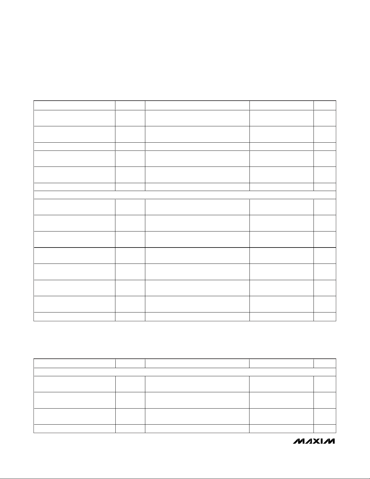
SWITCHING CHARACTERISTICS (VCC= +5V ±10%)
(TA= T
MIN
to T
MAX
, unless otherwise noted. Typical values are at VCC= +5V and TA= +25°C.)
)
)
Driver Disable Time from
Output High
Driver Enable Time from
Shutdown to Output High
D r i ver E nab l e Ti m e to Outp ut Low t
Driver Disable Time from
Output Low
Driver Enable Time from
Shutdown to Output Low
Driver Time to Shutdown t
RECEIVER
Receiver Propagation Delay
Receiver Output Skew t
Receiver Enable Time to
Output High
Receiver Disable Time from
Output High
Receiver Wake Time from
Shutdown
Receiver Enable Time to
Output Low
Receiver Disable Time from
Output Low
Receiver Time to Shutdown t
PARAMETER SYMBOL CONDITION MIN TYP MAX UNITS
t
DHZ
t
DZH(SHDN
DZL
t
DLZ
t
DZL(SHDN
SHDN
t
RPLH
t
RPHL
RSKEW
t
RZH
t
RHZ
t
RWAKERL
t
RZL
t
RLZ
SHDN
RL = 500Ω, CL = 50pF, Figure 4 1000 ns
RL = 500Ω, CL = 50pF, Figure 4 8 µs
RL = 500Ω, CL = 50pF, Figure 5 1500 ns
RL = 500Ω, CL = 50pF, Figure 5 2000 ns
RL = 500Ω, CL = 50pF, Figure 5 8 µs
RL = 500Ω, CL = 50pF 12 µs
,
CL = 20pF, VID = 2V, VCM = 0V,
Figure 6
CL = 20pF, t
Figure 6
RL = 1kΩ, CL = 20pF, Figure 7 1000 ns
RL = 1kΩ, CL = 20pF, Figure 7 150 ns
= 1kΩ, CL = 20pF, Figure 7 5 µs
RL = 1kΩ, CL = 20pF, Figure 7 1000 ns
RL = 1kΩ, CL = 20pF, Figure 7 150 ns
RL = 500Ω, CL = 50pF 200 ns
RSKEW
= [t
RPLH
- t
RPHL
2000 ns
],
200 ns
DRIVER
Driver Differential Propagation
Delay
Driver Differential Output
Transition Time
Differential Driver Output Skew t
Maximum Data Rate f
PARAMETER SYMBOL CONDITION MIN TYP MAX UNITS
t
,
DPLH
t
DPHL
, t
t
LH
DSKEW
MAX
RL = 54Ω, CL = 50pF, Figure 3 800 ns
HLRL
= 54Ω, CL = 50pF, Figure 3 100 1200 ns
RL = 54Ω, CL = 50pF, t
], Figure 3
t
DPHL
DSKEW
= [t
DPLH
-
500 kbps
200 ns
Page 5
MAX13448E
±80V Fault-Protected Full-Duplex
RS-485 Transceiver
_______________________________________________________________________________________ 5
SWITCHING CHARACTERISTICS (VCC= +5V ±10%) (continued)
(TA= T
MIN
to T
MAX
, unless otherwise noted. Typical values are at VCC= +5V and TA= +25°C.)
)
)
Note 2: Parameters are 100% production tested at TA= +25°C, unless otherwise noted. Limits over temperature are guaranteed by
design.
Note 3: All currents into the device are positive. All currents out of the device are negative. All voltages are referenced to device
ground, unless otherwise noted.
Note 4: ΔV
OD
and ΔVOCare the changes in VODand VOC, respectively, when the DI input changes state.
Note 5: The short-circuit output current applies to peak current just prior to foldback current limiting. The short-circuit foldback output
current applies during current limiting to allow a recover from bus contention.
D r i ver E nab l e Ti m e to Outp ut H i g ht
Driver Disable Time from
Output High
Driver Enable Time from
Shutdown to Output High
Driver Enable Time to Output Low t
Driver Disable Time from
Output Low
Driver Enable Time from
Shutdown to Output Low
Driver Time to Shutdown t
RECEIVER
Receiver Propagation Delay
Receiver Output Skew t
Receiver Enable Time to
Output High
Receiver Disable Time from
Output High
Receiver Wake Time from
Shutdown
Receiver Enable Time to
Output Low
Receiver Disable Time from
Output Low
Receiver Time to Shutdown t
PARAMETER SYMBOL CONDITION MIN TYP MAX UNITS
DZH
t
DHZ
t
DZH(SHDN
DZL
t
DLZ
t
DZL(SHDN
SHDN
t
RPLH
t
RPHL
RSKEW
t
RZH
t
RHZ
t
RWAKERL
t
RZL
t
RLZ
SHDN
RL = 500Ω, CL = 50pF, Figure 4 1500 ns
RL = 500Ω, CL = 50pF, Figure 4 1000 ns
RL = 500Ω, CL = 50pF, Figure 4 8 µs
RL = 500Ω, CL = 50pF, Figure 5 1000 ns
RL = 500Ω, CL = 50pF, Figure 5 2 µs
RL = 500Ω, CL = 50pF, Figure 5 8 µs
RL = 500Ω, CL = 50pF 12 µs
,
CL = 20pF, VID = 2V, VCM = 0V,
Figure 6
CL = 20pF, t
Figure 6
RL = 1kΩ, CL = 20pF, Figure 7 1000 ns
RL = 1kΩ, CL = 20pF, Figure 7 150 ns
= 1kΩ, CL = 20pF, Figure 7 8 µs
RL = 1kΩ, CL = 20pF, Figure 7 1000 ns
RL = 1kΩ, CL = 20pF, Figure 7 150 ns
RL = 500Ω, CL = 50pF 150 ns
RSKEW
= [t
RPLH
- t
RPHL
],
2000 ns
200 ns
Page 6

MAX13448E
±80V Fault-Protected Full-Duplex
RS-485 Transceiver
6 _______________________________________________________________________________________
Typical Operating Characteristics
(V
CC
= +3.3V, TA = +25°C, unless otherwise noted.)
SUPPLY CURRENT vs. TEMPERATURE
TEMPERATURE (°C)
SUPPLY CURRENT (mA)
MAX13448E toc01
-40 -15 10 35 60 85
4.05
4.10
4.15
4.20
DE = RE = LOW
A - B = HIGH
DI = FLOATING
RECEIVER OUTPUT SOURCE CURRENT
vs. OUTPUT HIGH VOLTAGE
OUTPUT SOURCE CURRENT (mA)
OUTPUT HIGH VOLTAGE (V)
MAX13448E toc02
0246810
2.0
2.2
2.4
2.6
2.8
3.0
3.2
3.4
DE = RE = LOW
A - B = HIGH
+25°C
+85°C
-40°C
RECEIVER OUTPUT SINK CURRENT
vs. OUTPUT LOW VOLTAGE
OUTPUT SINK CURRENT (mA)
OUTPUT LOW VOLTAGE (V)
MAX13448E toc03
0246810
0
0.1
0.2
0.3
0.4
0.5
0.6
0.7
0.8
0.9
DE = RE = LOW
B - A = HIGH
+85°C
+25°C
-40°C
RECEIVER OUTPUT HIGH VOLTAGE
vs. TEMPERATURE
TEMPERATURE (°C)
OUTPUT HIGH VOLTAGE (V)
MAX13448E toc04
-40 -15 10 35 60 85
3.20
3.21
3.22
3.23
3.24
3.25
DE = RE = LOW
A - B = HIGH
I
SOURCE
= 1mA
RECEIVER OUTPUT LOW VOLTAGE
vs. TEMPERATURE
TEMPERATURE (°C)
OUTPUT LOW VOLTAGE (V)
MAX13448E toc05
-40 -15 10 35 60 85
0.040
0.045
0.050
0.055
0.060
0.065
0.070
0.075
DE = RE = LOW
B - A = HIGH
I
SINK
= 1mA
DRIVER DIFFERENTIAL OUTPUT VOLTAGE
vs. DIFFERENTIAL OUTPUT CURRENT
DIFFERENTIAL OUTPUT CURRENT (mA)
DIFFERENTIAL OUTPUT VOLTAGE (V)
MAX13448E toc06
0 20406080100
1.0
1.5
2.0
2.5
3.0
3.5
DE = RE = HIGH
DI = HIGH
DRIVER DIFFERENTIAL OUTPUT
VOLTAGE vs. TEMPERATURE
1.94
1.92
1.90
1.88
DIFFERENTIAL OUTPUT VOLTAGE (V)
1.86
DE = RE = HIGH
DI = HIGH
= 54Ω
R
LOAD
-40 -15 10 35 60 85
TEMPERATURE (°C)
MAX13448E toc07
Page 7

MAX13448E
±80V Fault-Protected Full-Duplex
RS-485 Transceiver
_______________________________________________________________________________________ 7
Typical Operating Characteristics (continued)
(V
CC
= +3.3V, TA = +25°C, unless otherwise noted.)
SINGLE-ENDED DRIVER OUTPUT
HIGH VOLTAGE vs. SOURCE CURRENT
OUTPUT SOURCE CURRENT (mA)
OUTPUT HIGH VOLTAGE (V)
MAX13448E toc08
0246810
3.10
3.15
3.20
3.25
3.30
3.35
DE = RE = HIGH
DI = HIGH
SINGLE-ENDED DRIVER SINK CURRENT
vs. OUTPUT LOW VOLTAGE
OUTPUT SINK CURRENT (mA)
OUTPUT LOW VOLTAGE (V)
MAX13448E toc09
0246810
0
0.02
0.04
0.06
0.08
0.10
0.12
DE = RE = HIGH
DI = HIGH
SHUTDOWN CURRENT vs. TEMPERATURE
TEMPERATURE (°C)
SHUTDOWN CURRENT (μA)
MAX13448E toc10
-40 -15 10 35 60 85
0
5
10
15
20
25
30
400ns
DRIVER PROPAGATION DELAY (500kbsp)
2V/div
1V/div
MAX13448E toc11
DRIVER PROPAGATION DELAY
vs. TEMPERATURE
TEMPERATURE (°C)
PROPAGATION DELAY (ns)
MAX13448E toc13
-40 -15 10 35 60 85
300
350
400
450
500
DE = RE = HIGH
R
LOAD
= 54Ω
C
LOAD
= 50pF
t
DPLH
t
DPHL
RECEIVER PROPAGATION DELAY (500kbsp)
MAX13448E toc12
1V/div
2V/div
400ns
RECEIVER PROPAGATION DELAY
vs. TEMPERATURE
400
DE = RE = LOW
= 20pF
C
LOAD
375
350
PROPAGATION DELAY (ns)
325
300
-40 -15 10 35 60 85
t
RPLH
t
RPHL
TEMPERATURE (°C)
MAX13448E toc14
Page 8

MAX13448E
±80V Fault-Protected Full-Duplex
RS-485 Transceiver
8 _______________________________________________________________________________________
Figure 1. Driver DC Test Load
Figure 2. Driver Timing Test Circuit
Figure 3. Driver Propagation Delays
Pin Description
PIN NAME FUNCTION
1, 8, 13 N.C. No Connection. Not internally connected. Connect N.C. to GND or leave it unconnected.
2 RO Receiver Output. If receiver is enabled and (A - B) ≥ -50mV, RO = high; if (A - B) ≥ -200mV, RO = low.
3 RE
4DE
5DI
6, 7 GND Ground
9 Y Noninverting Driver Output
10 Z Inverting Driver Output
11 B Inverting Receiver Input
12 A Noninverting Receiver Input
14 V
CC
Receiver Output Enable. Drive RE low to enable RO; RO is high impedance when RE is high. Drive
RE high and DE low to enter low-power shutdown mode.
Driver Output Enable. Drive DE high to enable the driver outputs. Drive DE low to put the outputs in
high impedance. Drive RE high and DE low to enter low-power shutdown mode.
Driver Input. Drive DI low to force the noninverting output low and the inverting output high. Drive DI
high to force the noninverting output high and the inverting output low.
Positive Supply. VCC = +3.0V to +5.5V. Bypass VCC to GND with a 1µF ceramic capacitor as close
to V
as possible. Typical VCC values are at VCC = +3.3V and VCC = +5.0V.
CC
Y
V
OD
Z
V
CC
DE
DI
Y
V
O
Z
RL/2
RL/2
V
CC
DI
VCC/2
0
Z
V
V
OC
V
OD
C
L
R
L
C
L
O
Y
1/2 V
O
V
O
0
10%
-V
O
t
LH
t
DPLH
VOD = V (Y) - V (Z)
90%
t
SKEW = |tDPLH - tDPHL
|
t
DPHL
1/2 V
O
90%
t
HL
10%
Page 9

MAX13448E
±80V Fault-Protected Full-Duplex
RS-485 Transceiver
_______________________________________________________________________________________ 9
Figure 4. Driver Enable and Disable Times (t
DHZ
, t
DZH
, t
DZH(SHDN)
)
Figure 5. Driver Enable and Disable Times (t
DLZ
, t
DZL
, t
DZL(SHDN)
)
0 OR V
GENERATOR
DE
t
, t
DZH
DZH(SHDN)
OUT
D1
CC
VOM = (0 + VOH)/2
D
50Ω
Y
S1
OUT
R
t
DHZ
= 500Ω
L
VCC/2
0.25V
V
CC
0
V
OH
0
Z
C
L
50pF
0 OR V
GENERATOR
DE
, t
t
DZL
DZL(SHDN)
V
CC
OUT
V
OL
D1
CC
50Ω
VOM = (VOL + VCC)/2
V
CC
= 500Ω
R
Y
S1
D
D
Z
C
L
50pF
L
OUT
V
CC
VCC/2
0
t
DLZ
0.25V
Page 10

MAX13448E
±80V Fault-Protected Full-Duplex
RS-485 Transceiver
10 ______________________________________________________________________________________
Figure 6. Receiver Propagation Delays
Figure 7. Receiver Enable and Disable Times
B
A
V
ID
B
0
RE
RO
R
+1.5V
-1.5V
S1 OPEN
S2 CLOSED
S3 = +1.5V
RO
C
L
20pF
A
t
RPLH
V
OH
RO
V
OL
VOH + V
t
SKEW
OL
2
= |t
RPLH
t
RPHL
- t
|
RPHL
S1
S3
A
B
GENERATOR
C
L
20pF
1kΩ
S2
V
ID
RO
R
R
RE
50Ω
S1 CLOSED
S2 OPEN
V
CC
S3 = -1.5V
V
CC
V
CC
VCC/2
0
t
, t
*
RZH
RWAKE
V
OH
VOH/2
0
RE
t
RZL
(V
RO
, t
SHDN
+ VCC)/2
OL
0
*
V
CC
V
OL
S1 OPEN
S2 CLOSED
S3 = +1.5V
V
/2
RE
CC
t
, t
*
RHZ
SHDN
V
CC
0
V
OH
RE
t
RLZ
S1 CLOSED
S2 OPEN
S3 = -1.5V
/2
V
CC
, t
SHDN
*
0.25V
RO
0
RO
0.25V
V
CC
0
V
CC
*DE =
LOW
V
OL
Page 11

MAX13448E
Detailed Description
The MAX13448E ±80V fault-protected RS-485/RS-422
transceiver contains one driver and one receiver. This
device features fail-safe circuitry, guaranteeing a logichigh receiver output when the receiver inputs are open
or shorted, or when they are connected to a terminated
transmission line with all drivers disabled. The device
has a hot-swap input structure that prevents disturbances on the differential signal lines when a circuit
board is plugged into a hot backplane. All receiver
inputs and driver outputs are protected to ±8kV ESD
using the Human Body Model. The MAX13448E
features a reduced slew-rate driver that minimizes
EMI and reduces reflections caused by improperly
terminated cables, allowing error-free data transmission up to 500kbps.
Driver
The driver accepts a single-ended, logic-level input
(DI) and converts it to a differential, RS-485/RS-422
level output (A and B). Deasserting the driver enable
places the driver outputs (A and B) into a high-impedance state.
Receiver
The receiver accepts a differential, RS-485/RS-422
level input (A and B), and translates it to a singleended, logic-level output (RO). Deasserting the receiver enable places the receiver outputs (RO) into a
high-impedance state (see Table 1).
Low-Power Shutdown
Low-power shutdown is initiated by bringing DE low
and RE high. In shutdown, the device draws a maximum of 100µA of supply current.
The device is guaranteed to not enter shutdown if DE is
low and RE is high for 1µs. If the inputs are in this state
for at least 1ms, the device is guaranteed to enter shutdown. In the shutdown state, the driver outputs (A and
B) as well as the receiver output (RO) are in a highimpedance state.
±80V Fault Protection
In certain applications, such as industrial control, driver
outputs and receiver inputs of an RS-485 device sometimes experience common-mode voltages in excess of
the -7V to +12V range specified in the EIA/TIA-485
standard. In these applications, ordinary RS-485
devices (typical absolute maximum ratings of -8V to
+12.5V) may experience damage without the addition
of external protection devices.
To reduce system complexity and the need for external
protection, the driver outputs and receiver inputs of the
MAX13448E withstand voltage faults of up to ±80V with
respect to ground without damage (see the
Absolute
Maximum Ratings
section, Note 1). Protection is guaranteed regardless of whether the device is active, in
shutdown, or without power. Certain parasitic effects
present while driving an unterminated cable may cause
the voltage seen at driver outputs to exceed the
absolute maximum limit, while the DI input is switched
during a ±80V fault on the A or B input. Therefore, a
termination resistor is recommend in order to maximize
the overvoltage fault protection while the DI input is
being switched. If the DI input does not change state
while the fault voltage is present, the MAX13448E will
withstand up the ±80V on the RS-485 inputs, regardless of the presence of a termination resistor. While the
MAX13448E is not damaged by up to ±80V commonmode voltages, the RO, Y, and Z outputs will be in an
indeterminate state if the common-mode voltage
exceeds -7V to +12V.
True Fail-Safe
The MAX13448E guarantees a logic-high receiver output when the receiver inputs are shorted or open, or
when they are connected to a terminated transmission
line with all drivers disabled. This is done by setting the
±80V Fault-Protected Full-Duplex
RS-485 Transceiver
______________________________________________________________________________________ 11
X = Don’t care; shutdown mode, driver, and receiver outputs are
high impedance.
Table 1. Function Table
TRANSMITTING
INPUT OUTPUT
RE DE DI Z Y
X10 1 0
X11 0 1
00X
1 0 X High Impedance (Shutdown)
RECEIVING
INPUT OUTPUT
RE DE A - B RO
0 X -50mV 1
0 X -200mV 0
1 1 X Disabled
1 0 X High Impedance (Shutdown)
High
Impedance
High
Impedance
Page 12

MAX13448E
±80V Fault-Protected Full-Duplex
RS-485 Transceiver
12 ______________________________________________________________________________________
Figure 8a. Human Body ESD Test Model
Figure 8b. Human Body Current Waveform
receiver threshold between -50mV and -200mV. If the
differential receiver input voltage (A - B) is greater than
or equal to -50mV, RO is logic-high. If A - B is less than
or equal to -200mV, RO is logic-low. In the case of a
terminated bus with all transmitters disabled, the
receiver’s differential input voltage is pulled to 0V by
the termination. With the receiver thresholds of the
MAX13448E, this results in a logic-high with a 50mV
minimum noise margin. The -50mV to -200mV threshold
complies with the ±200mV EIA/TIA-485 standard.
±8kV ESD Protection
As with all Maxim devices, ESD-protection structures
are incorporated on all pins to protect against electrostatic discharges encountered during handling and
assembly. The driver outputs and receiver inputs of the
MAX13448E have extra protection against static electricity. Maxim’s engineers have developed state-of-theart structures to protect these pins against ESD of ±8kV
without damage. The ESD structures withstand high
ESD in all states: normal operation, shutdown, and
powered down. After an ESD event, the MAX13448E
keeps working without latchup or damage. ESD protection can be tested in various ways. The transmitter outputs and receiver inputs of the MAX13448E are
characterized for protection to the following limits:
• ±8kV using the Human Body Model
ESD Test Conditions
ESD performance depends on a variety of conditions.
Contact Maxim for a reliability report that documents
test setup, test methodology, and test results.
Human Body Model
Figure 8a shows the Human Body Model, and Figure
8b shows the current waveform it generates when discharged into a low impedance. This model consists of a
100pF capacitor charged to the ESD voltage of interest,
which is then discharged into the test device through a
1.5kΩ resistor.
Driver Output Protection
Two mechanisms prevent excessive output current and
power dissipation caused by faults or by bus contention. The first, a foldback current limit on the output
stage, provides immediate protection against short
circuits over the whole common-mode voltage range
(see the
Typical Operating Characteristics
). The second, a thermal-shutdown circuit, forces the driver outputs into a high-impedance state if the die temperature
exceeds +160°C (typ).
Hot-Swap Capability
Hot-Swap Inputs
When circuit boards are inserted into a powered backplane, disturbances to the data bus can lead to data
errors. Upon initial circuit-board insertion, the data
communication processor undergoes its own power-up
sequence. During this period, the processor’s logicoutput drivers are high impedance and are unable to
drive the DE input of the device to a defined logic level.
Leakage currents up to ±10µA from the high-impedance state of the processor’s logic drivers could cause
standard CMOS enable inputs of a transceiver to drift to
an incorrect logic level. Additionally, parasitic circuitboard capacitance could cause coupling of VCCor
GND to the enable inputs. Without the hot-swap capability, these factors could improperly enable the transceiver’s driver or receiver.
When VCCrises, an internal pulldown circuit holds DE
low. After the initial power-up sequence, the pulldown
circuit becomes transparent, resetting the hot-swap
tolerable input.
HIGH-
VOLTAGE
DC
SOURCE
R
C
1MΩ
CHARGE-CURRENT-
LIMIT RESISTOR
C
100pF
s
R
D
1500Ω
DISCHARGE
RESISTANCE
STORAGE
CAPACITOR
DEVICE
UNDER
TEST
AMPS
IP 100%
90%
36.8%
10%
0
0
PEAK-TO-PEAK RINGING
I
r
(NOT DRAWN TO SCALE)
t
RL
TIME
t
DL
CURRENT WAVEFORM
Page 13

MAX13448E
±80V Fault-Protected Full-Duplex
RS-485 Transceiver
______________________________________________________________________________________ 13
Hot-Swap Input Circuitry
The enable inputs feature hot-swap capability. At the
input there are two NMOS devices, M1 and M2 (Figure
9). When V
CC
ramps from zero, an internal 7µs timer
turns on M2 and sets the SR latch that also turns on M1.
Transistor M2, a 1.5mA current sink, and M1, a 100µA
current sink, pull DE to GND through a 5kΩ resistor. M2
is designed to pull DE to the disabled state against an
external parasitic capacitance up to 100pF that can
drive DE high. After 7µs, the timer deactivates M2 while
M1 remains on, holding DE low against three-state leakages that can drive DE high. M1 remains on until an
external source overcomes the required input current.
At this time, the SR latch resets and M1 turns off. When
M1 turns off, DE reverts to a standard, high-impedance
CMOS input.
Applications Information
256 Transceivers on the Bus
The RS-485 standard specifies the load each receiver
places on the bus in terms of unit loads. An RS-485
compliant transmitter can drive 32 one-unit loads when
used with a 120Ω cable that is terminated on both ends
over a common-mode range of -7V to +12V. The
MAX13448E is specified as 1/8 unit loads. This means
a compliant transmitter can drive up to 256 MAX13448E
devices. Reducing the common mode and/or changing
the characteristic impedance of the cable changes the
maximum number of receivers that can be used. Refer
to the TIA/EIA-485 specification for further details.
Proper Termination and Cabling/Wiring
Configurations
When the data rates for RS-485 are high relative to its
cable lengths, the system is subject to proper transmission line design. In most cases, a single, controlledimpedance cable or trace should be used and should be
properly terminated on both ends with the characteristic
impedance of the cable/trace. RS-485 transceivers
should be connected to the cable/traces with minimum
length wires to prevent stubs. Star configurations and
improperly terminated cables can cause data loss. Refer
to the
Applications
section of the Maxim website or to
TIA/EIA publication TSB89 for further information.
Reduced EMI and Reflections
The MAX13448E features reduced slew-rate drivers
that minimize EMI and reduce reflections caused by
improperly terminated cables, allowing error-free data
transmission up to 500kbps.
Line Length
The Telecommunications Industry Association (TIA)
publishes the document TSB-89:
Application
Guidelines for TIA/EIA-485-A
that is a good reference
for determining maximum data rate vs. line length.
Typical Applications
The MAX13448E transceivers are designed for bidirectional data communications on multipoint bus transmission lines. Figure 10 shows a typical network application
circuit. To minimize reflections, terminate the line at both
ends in its characteristic impedance, and keep stub
lengths off the main line as short as possible.
Figure 9. Simplified Structure of the Driver Enable Pin (DE)
V
CC
100μA
500μA
10μs
SR LATCH
DE
(HOT SWAP)
M2M1
TIMER
TIMER
5kΩ
DE
Page 14

Chip Information
PROCESS: BiCMOS
Figure 10. Typical Full-Duplex RS-485 Network
Pin Configuration
PACKAGE TYPE PACKAGE CODE DOCUMENT NO.
14 SO S14-5
21-0041
Package Information
For the latest package outline information and land patterns, go
to www.maxim-ic.com/packages
.
MAX13448E
±80V Fault-Protected Full-Duplex
RS-485 Transceiver
Maxim cannot assume responsibility for use of any circuitry other than circuitry entirely embodied in a Maxim product. No circuit patent licenses are
implied. Maxim reserves the right to change the circuitry and specifications without notice at any time.
14
____________________Maxim Integrated Products, 120 San Gabriel Drive, Sunnyvale, CA 94086 408-737-7600
© 2008 Maxim Integrated Products is a registered trademark of Maxim Integrated Products, Inc.
A
RO
RE
DE
DI
R
D
B
Z
Y
TOP VIEW
N.C.
+
120Ω
120Ω
YZBA
D
DI
DE
RE
141
V
CC
Y
120Ω
Z
B
120Ω
A
YZBA
R
D
RO
DI
R
MAX13448E
DE
RO
RE
D
R
DI
DE
RE
RO
132 N.C.RO
MAX13448E
SO
123ARE
114BDE
105ZDI
96YGND
87 N.C.GND
 Loading...