

General Description
The MAX13430E–MAX13433E are full- and half-duplex
RS-485 transceivers that feature an adjustable low-voltage logic interface for operation in multivoltage systems.
This allows direct interfacing to low-voltage ASIC/FPGAs
without extra components. The MAX13430E–MAX13433E
RS-485 transceivers operate with a VCCvoltage supply
from +3V to +5V. The low-voltage logic interface operates
with a voltage supply from +1.62V to VCC.
The MAX13430E/MAX13432E feature reduced slewrate drivers that minimize EMI and reduce reflections
caused by improperly terminated cables, allowing
error-free data transmission up to 500kbps. The
MAX13431E/MAX13433E driver slew rates are not limited, enabling data transmission up to 16Mbps. The
MAX13430E/MAX13431E are intended for half-duplex
communications, and the MAX13432E/MAX13433E are
intended for full-duplex communications.
The MAX13430E/MAX13431E are available in 10-pin
µMAX®and 10-pin TDFN packages. The MAX13432E/
MAX13433E are available in 14-pin TDFN and 14-pin
SO packages.
Features
♦ Wide +3V to +5V Input Supply Range
♦ Low-Voltage Logic Interface +1.62V (min)
♦ Ultra-Low Supply Current in Shutdown Mode
10µA ICC(max), 1µA IL(max)
♦ Thermal Shutdown Protection
♦ Hot-Swap Input Structures on DE and RE
♦ 1/8-Unit Load Allows Up to 256 Transceivers on
the Bus
♦ Enhanced Slew-Rate Limiting
(MAX13430E/MAX13432E)
♦ Extended ESD Protection for RS-485 I/O Pins
±30kV Human Body Model
±15kV Air-Gap Discharge per IEC 61000-4-2
±10kV Contact Discharge per IEC 61000-4-2
♦ Extended -40°C to +85°C Operating Temperature
Range
♦ Space-Saving TDFN and µMAX Packages
MAX13430E–MAX13433E
RS-485 Transceivers with Low-Voltage
Logic Interface
________________________________________________________________
Maxim Integrated Products
1
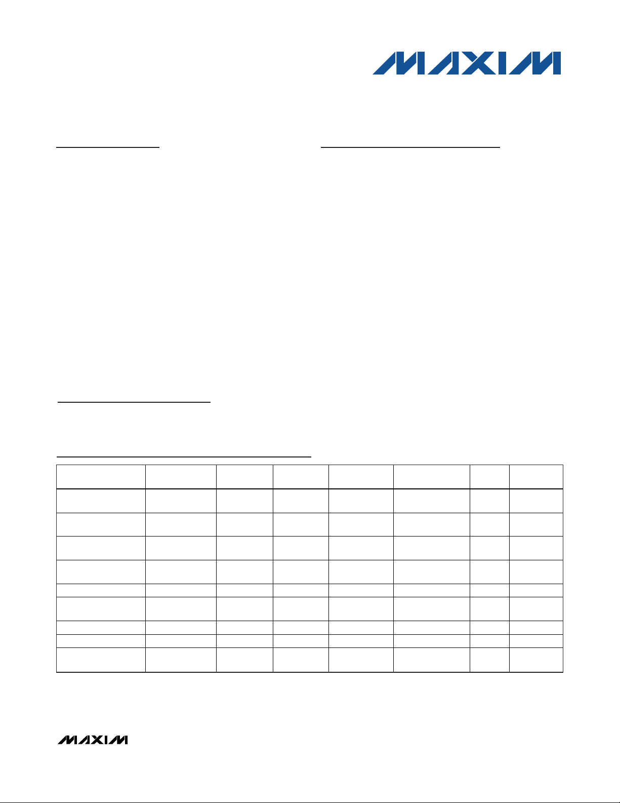
Ordering Information/Selector Guide
19-4322; Rev 2; 5/10
For pricing, delivery, and ordering information, please contact Maxim Direct at 1-888-629-4642,
or visit Maxim’s website at www.maxim-ic.com.
PART PIN-PACKAGE
FULL/HALF
DUPLEX
DATA RATE
(Mbps)
SLEW RATE
LIMITED
TRANSCEIVERS
ON BUS
TOP
MARK
PACKAGE
CODE
MAX13430EETB+
10 TDFN-EP*
(3mm x 3mm)
Half 0.5 Yes 256 AUS T1033-1
MAX13430EEUB+
10 μMAX
(3mm x 3mm)
Half 0.5 Yes 256 — U10-2
MAX13431EETB+
10 TDFN-EP*
(3mm x 3mm)
Half 16 No 256 AUT T1033-1
MAX13431EEUB+
10 μMAX
(3mm x 3mm)
Half 16 No 256 — U10-2
MAX13432EESD+ 14 SO Ful l 0.5 Yes 256 — S14-1
MAX13432EETD+
14 TDFN-EP*
(3mm x 3mm)
Ful l 0.5 Yes 256 AEG T1433-2
MAX13433EESD+ 14 SO Ful l 16 No 256 — S14-1
MAX13433EESD/V+ 14 SO Ful l 16 No 256 — S14-1
MAX13433EETD+
14 TDFN-EP*
(3mm x 3mm)
Ful l 16 No 256 AEH T1433-2
Typical Application Circuits appears at end of data sheet.
Note: All devices are specified over the extended -40°C to +85°C operating temperature range.
+
Denotes a lead(Pb)-free/RoHS-compliant package.
*
EP = Exposed pad.
/V denotes an automotive qualified part.
µMAX is a registered trademark of Maxim Integrated Products, Inc.
Applications
Industrial Control Systems
Portable Industrial
Equipment
Motor Control
HVAC
MAX13430E–MAX13433E
RS-485 Transceivers with Low-Voltage
Logic Interface
2 _______________________________________________________________________________________
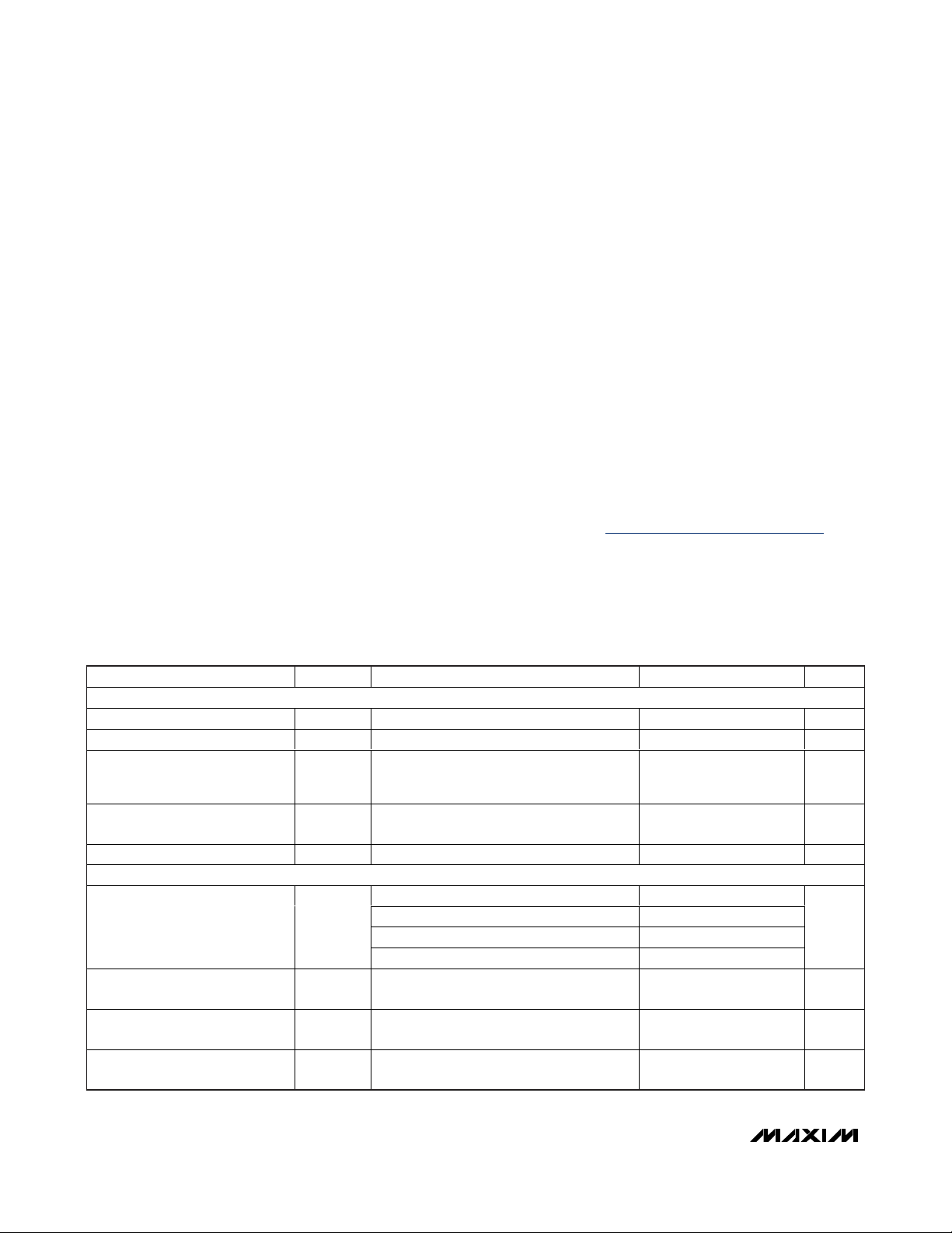
ABSOLUTE MAXIMUM RATINGS
DC ELECTRICAL CHARACTERISTICS
(VCC= +3V to +5.5V, VL= +1.8V to VCC, TA= -40°C to +85°C, unless otherwise noted. Typical values are VCC= +5V, VL= +1.8V at
T
A
= +25°C.) (Notes 2, 3)
Stresses beyond those listed under “Absolute Maximum Ratings” may cause permanent damage to the device. These are stress ratings only, and functional
operation of the device at these or any other conditions beyond those indicated in the operational sections of the specifications is not implied. Exposure to
absolute maximum rating conditions for extended periods may affect device reliability.
Note 1: Package thermal resistances were obtained using the method described in JEDEC specification JESD51-7, using a four-
layer board. For detailed information on package thermal considerations, refer to www.maxim-ic.com/thermal-tutorial
.
(All voltages referenced to GND.)
Supply Voltage (V
CC
) ...............................................-0.3V to +6V
Logic Supply Voltage (V
L )
......................................-0.3V to +6V
Control Input Voltage (RE) .............................-0.3V to (V
L
+0.3V)
Control Input Voltage (DE) ......................................-0.3V to +6V
Driver Input Voltage (DI) ..........................................-0.3V to +6V
Driver Output Voltage (Y, Z, A, B) ............................-8V to +13V
Receiver Input Voltage (A, B)
(MAX13430E/MAX13431E)....................................-8V to +13V
Receiver Input Voltage (A, B)
(MAX13432E/MAX13433E)..................................-25V to +25V
Receiver Output Voltage (RO) .....................-0.3V to (V
L
+ 0.3V)
Driver Output Current ....................................................±250mA
Short-Circuit Duration (RO, A, B) to GND .................Continuous
Power Dissipation (T
A
= +70°C)
10-Pin µMAX (derate 8.8mW/°C above +70°C) ..........707mW
10-Pin TDFN (derate 24.4mW/°C above +70°C) ......1951mW
14-Pin TDFN (derate 24.4mW/°C above +70°C) ......1951mW
14-Pin SO (derate 11.9mW/°C above +70°C) .............952mW
Junction-to-Ambient Thermal Resistance (θ
JA
) (Note 1)
10-Pin µMAX ...........................................................113.1°C/W
10-Pin TDFN.................................................................41°C/W
14-Pin TDFN ................................................................41°C/W
14-Pin SO ....................................................................84°C/W
Junction-to-Ambient Thermal Resistance (θ
JC
) (Note 1)
10-Pin µMAX ................................................................42°C/W
10-Pin TDFN...................................................................9°C/W
14-Pin TDFN ..................................................................8°C/W
14-Pin SO ....................................................................34°C/W
Operating Temperature Range ...........................-40°C to +85°C
Junction Temperature..................................................... +150°C
Storage Temperature Range .............................-65°C to +150°C
Lead Temperature (soldering, 10s) .................................+300°C
Soldering Temperature (reflow) .......................................+260°C
PARAMETER SYMBOL CONDITIONS MIN TYP MAX UNITS
POWER SUPPLY
VCC Supply-Voltage Range V
VL Supply-Voltage Range V
ICC Supply Current I
ICC Supply Current in Shutdown
Mode
VL Supply Current I
DRIVER
Differential Driver Output
(Figure 1)
Change in Magnitude of
Differential Output Voltage
Driver Common-Mode Output
Voltage
Change in Magnitude of
Common-Mode Voltage
I
SHDN
V
ΔV
V
ΔV
CC
CC
OD
OC
L
DE = RE = high, no load
DE = RE = low, no load
DE = high, RE = low, no load
DE = low, RE = high, no load 10 µA
RO = no load 1 µA
L
RL = 100Ω, VCC = +3V 2 V
RL = 54Ω, VCC = +3V 1.5 V
RL = 100Ω, VCC = +4.5V 2.25 V
RL = 54Ω, VCC = +4.5V 2.25 V
RL = 100Ω or 54Ω, Figure 1 (Note 4) 0.2 V
OD
RL = 100Ω or 54Ω, Figure 1 VCC/2 3 V
RL = 100Ω or 54Ω, Figure 1 (Note 4) 0.2 V
OC
3 5.5 V
1.62 V
CC
2mA
CC
CC
CC
CC
V
V
MAX13430E–MAX13433E
RS-485 Transceivers with Low-Voltage
Logic Interface
_______________________________________________________________________________________ 3
DC ELECTRICAL CHARACTERISTICS (continued)
(VCC= +3V to +5.5V, VL= +1.8V to VCC, TA= -40°C to +85°C, unless otherwise noted. Typical values are VCC= +5V, VL= +1.8V at
T
A
= +25°C.) (Notes 2, 3)
Output Leakage Current
(Y and Z)
Driver Short-Circuit Output
Current (Note 5)
Driver Short-Circuit Output
Foldback Current (Note 5)
Thermal Shutdown Threshold T
Thermal Shutdown Hysteresis T
RECEIVER
Input Current (A and B) I
Receiver Differential Threshold
Voltage
Receiver Input Hysteresis ΔV
Receiver Input Resistance R
LOGIC INTERFACE
Input High Logic Level
(DI, DE, RE)
Input Low Logic Level
(DI, DE, RE)
Input Current (DI, DE, RE)I
Input Impedance on First
Transition
Output High Logic Level (RO) V
Output Low Logic Level (RO) V
Receiver Three-State Output
Current (RO)
Receiver Output Short-Circuit
Current (RO)
ESD PROTECTION
All Other Pins
(Except A, B, Y, and Z)
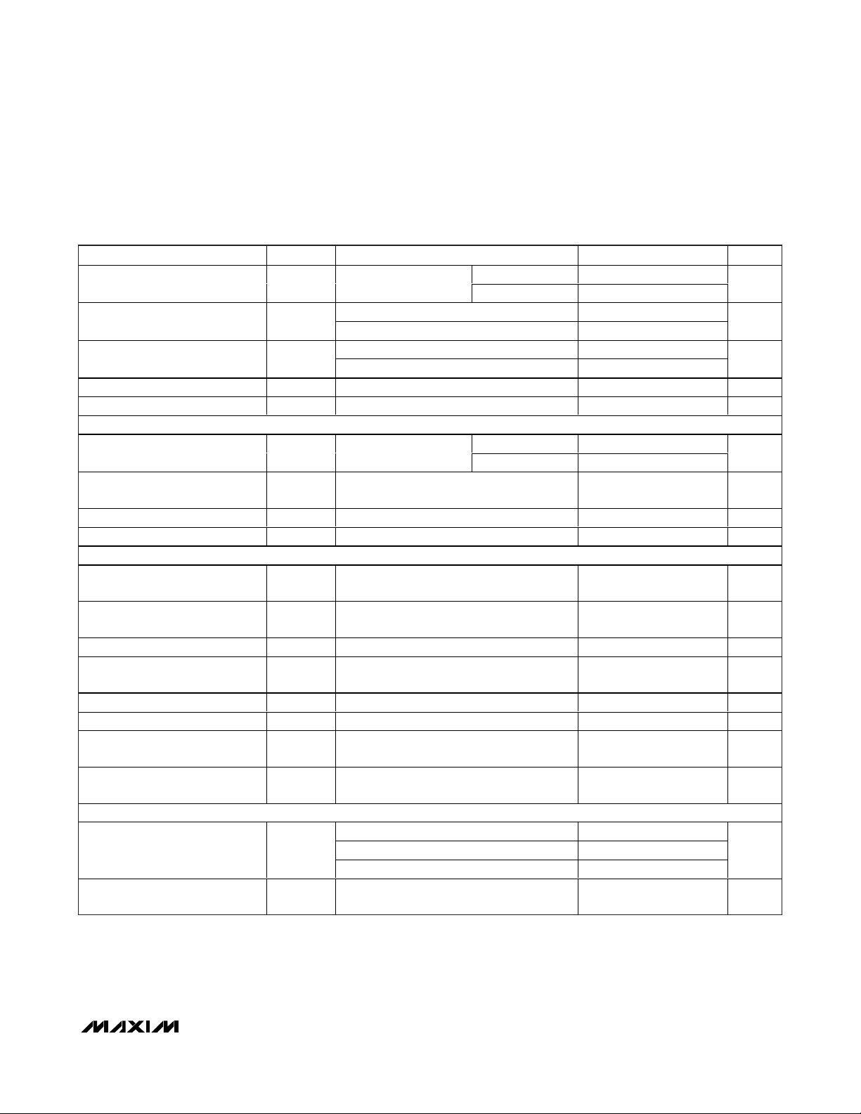
PARAMETER SYMBOL CONDITIONS MIN TYP MAX UNITS
I
OLK
I
OSD
I
OSDF
A, B
V
V
V
R
DE, RE
I
OZR
I
OSR
TS
TSH
TH
TH
IN
IH
IL
IN
OH
OL
DE = GND,
= V
V
CC
0 ≤ V
-7V ≤ V
(VCC - 1V) ≤ V
-7V ≤ V
or +5.5V
GND
≤ +12V +250
OUT
≤ V
OUT
CC
≤ +12V 15
OUT
≤ +1V -15
OUT
DE = GND,
= V
V
CC
GND
or +5.5V
-7V ≤ VCM ≤ +12V -200 -50 mV
VCM = 0 15 mV
-7V ≤ VCM ≤ +12V 96 kΩ
VDI = VDE = VRE = VL = +5.5V ±1 µA
IO = -1mA, VA - VB = V
IO = 1mA, VA - VB = -V
0 ≤ VRO ≤ V
0 ≤ VRO ≤ V
L
L
VIN = +12V 125
V
= -7V -100
IN
-250
+150 °C
15 °C
VCM = +12V 125
V
= -7V -100
CM
2/3 x
V
L
110kΩ
TH
TH
VL - 0.4 V
-1 0.01 +1 µA
-110 +110 mA
1/3 x
V
L
0.4 V
µA
mA
mA
µA
V
V
IEC 61000-4-2 Air Gap Discharge ±15
IEC 61000-4-2 Contact Discharge ±10A, B, Y, Z to GND
kV
Human Body Model ±30
Human Body Model ±2 kV
MAX13430E–MAX13433E
RS-485 Transceivers with Low-Voltage
Logic Interface
4 _______________________________________________________________________________________
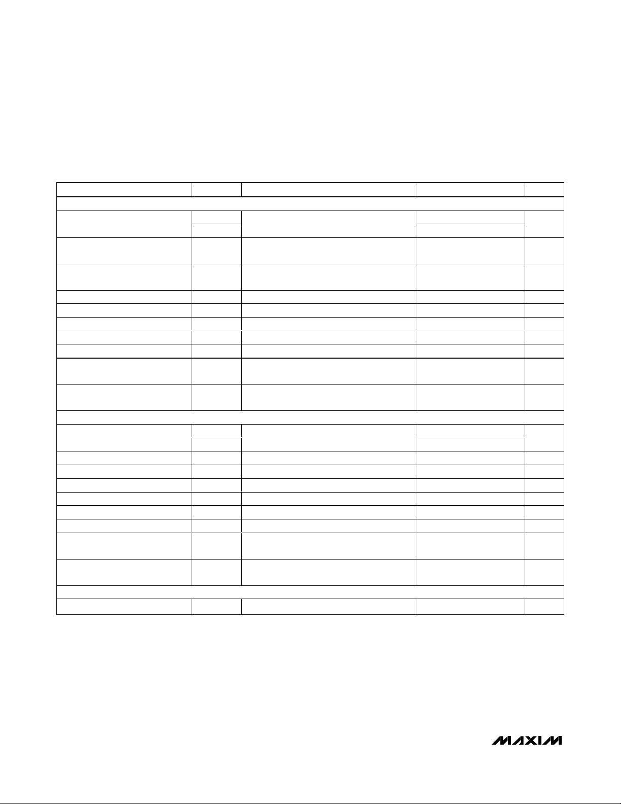
SWITCHING CHARACTERISTICS (MAX13431E/MAX13433E (16Mbps))
(VCC= +3V to +5.5V, VL= +1.8V to VCC, TA= -40°C to +85°C, unless otherwise noted. Typical values are VCC= +5V, VL= +1.8V at
T
A
= +25°C.) (Notes 2, 3)
)
)
)
)
PARAMETER SYMBOL CONDITIONS MIN TYP MAX UNITS
DRIVER
t
Driver Propagation Delay
(Figures 2 and 3)
Driver Differential Output Rise or
Fall Time
Differential Driver Output Skew
|t
- t
DPHL
|
DPLH
Maximum Data Rate 16 Mbps
Driver Enable to Output High t
Driver Enable to Output Low t
Driver Disable Time from Low t
Driver Disable Time from High t
Driver Enable from Shutdown
to Output High
Driver Enable from Shutdown
to Output Low
RECEIVER
Receiver Propagation Delay
(Figures 6 and 7)
Receiver Output Skew t
Maximum Data Rate 16 Mbps
Receiver Enable to Output Low t
Receiver Enable to Output High t
Receiver Disable Time from Low t
Receiver Disable Time from High t
Receiver Enable from
Shutdown to Output High
Receiver Enable from
Shutdown to Output Low
DRIVER/RECEIVER
Time to Shutdown t
DPLH
t
DPHL
t
, t
R
F
t
DSKEW
DZH
DZL
DLZ
DHZ
t
DZH(SHDN
t
DZL(SHDN
t
RPLH
t
RPHL
RSKEW
RZL
RZH
RLZ
RHZ
t
RZH(SHDN
t
RZL(SHDN
SHDN
CL = 50pF, R
CL = 50pF, RL = 54Ω, Figures 2 and 3 15 ns
CL = 50pF, RL = 54Ω, Figures 2 and 3 8 ns
CL = 50pF, RL = 500Ω, Figure 4 150 ns
CL = 50pF, RL = 500Ω, Figure 5 150 ns
CL = 50pF, RL = 500Ω, Figure 4 100 ns
CL = 50pF, RL = 500Ω, Figure 5 120 ns
CL = 50pF, RL = 500Ω, Figure 4 5 µs
CL = 50pF, RL = 500Ω, Figure 5 5 µs
CL = 15pF
CL = 15pF, Figures 6 and 7 13 ns
Figure 8 50 ns
Figure 8 50 ns
Figure 8 50 ns
Figure 8 50 ns
Figure 8 5 µs
Figure 8 5 µs
DIFF
= 54Ω
50 340 700 ns
50
50
80
80
ns
ns
MAX13430E–MAX13433E
RS-485 Transceivers with Low-Voltage
Logic Interface
_______________________________________________________________________________________ 5
SWITCHING CHARACTERISTICS (MAX13430E/MAX13432E (500kbps))
(VCC= +3V to +5.5V, VL= +1.8V to VCC, TA= -40°C to +85°C, unless otherwise noted. Typical values are VCC= +5V, VL= +1.8V at
T
A
= +25°C.) (Notes 2, 3)
)
)
)
)
PARAMETER SYMBOL CONDITIONS MIN TYP MAX UNITS
DRIVER
t
Driver Propagation Delay
(Figures 2 and 3)
Driver Differential Output Rise or
Fall Time
Differential Driver Output Skew
|t
- t
DPHL
|
DPLH
Maximum Data Rate 500 kbps
Driver Enable to Output High t
Driver Enable to Output Low t
Driver Disable Time from Low t
Driver Disable Time from High t
Driver Enable from Shutdown
to Output High
Driver Enable from Shutdown
to Output Low
RECEIVER
Receiver Propagation Delay
(Figures 6 and 7)
Receiver Output Skew t
Maximum Data Rate 500 kbps
Receiver Enable to
Output Low
Receiver Enable to
Output High
Receiver Disable Time
from Low
Receiver Disable Time
from High
Receiver Enable from
Shutdown to Output High
Receiver Enable from
Shutdown to Output Low
DPLH
t
DPHL
t
, t
R
F
t
DSKEW
DZH
DZL
DLZ
DHZ
t
DZH(SHDN
t
DZL(SHDN
t
RPLH
t
RPHL
RSKEW
t
RZL
t
RZH
t
RLZ
t
RHZ
t
RZH(SHDN
t
RZL(SHDN
CL = 50pF, RL = 54Ω
CL = 50pF, RL = 54Ω, Figures 2 and 3 200 800 ns
CL = 50pF, RL = 54Ω, Figures 2 and 3 100 ns
CL = 50pF, RL = 500Ω, Figure 4 2.5 µs
CL = 50pF, RL = 500Ω, Figure 5 2.5 µs
CL = 50pF, RL = 500Ω, Figure 4 100 ns
CL = 50pF, RL = 500Ω, Figure 5 120 ns
CL = 50pF, RL = 500Ω, Figure 4 5 µs
CL = 50pF, RL = 500Ω, Figure 5 5 µs
CL = 15pF
CL = 15pF, Figures 6 and 7 30 ns
Figure 8 50 ns
Figure 8 50 ns
Figure 8 50 ns
Figure 8 50 ns
Figure 8 5 µs
Figure 8 5 µs
180 800
180 800
200
200
ns
ns
MAX13430E–MAX13433E
RS-485 Transceivers with Low-Voltage
Logic Interface
6 _______________________________________________________________________________________
SWITCHING CHARACTERISTICS (MAX13430E/MAX13432E (500kbps)) (continued)
(VCC= +3V to +5.5V, VL= +1.8V to VCC, TA= -40°C to +85°C, unless otherwise noted. Typical values are VCC= +5V, VL= +1.8V at
T
A
= +25°C.) (Notes 2, 3)
Note 2: Parameters are 100% production tested at TA= +25°C, unless otherwise noted. Limits over temperature are guaranteed by
design.
Note 3: All currents into the device are positive. All currents out of the device are negative. All voltages are referenced to device
ground, unless otherwise noted.
Note 4: ΔV
OD
and ΔVOCare the changes in VODand VOC, respectively, when the DI input changes state.
Note 5: The short-circuit output current is the peak current just prior to current limiting; the short-circuit foldback output current
applies during current limiting to allow a recovery from bus contention.
Typical Operating Characteriststics
(V
CC
= +5V, VL = +5V, TA = +25°C, unless otherwise noted.)
OUTPUT CURRENT vs. RECEIVER
OUTPUT-HIGH VOLTAGE
MAX13430E-3E toc02
OUTPUT-HIGH VOLTAGE, VOH (V)
OUTPUT CURRENT FOR V
L
= 5V (mA)
OUTPUT CURRENT FOR V
L
= 1.8V (mA)
2134
20
40
60
0
30
50
10
2
4
6
0
3
5
1
05
VL = 1.8V
VL = 5V
OUTPUT CURRENT vs. RECEIVER
OUTPUT-LOW VOLTAGE
MAX13430E-3E toc03
OUTPUT-LOW VOLTAGE, VOL (V)
OUTPUT CURRENT FOR V
L
= 5V (mA)
OUTPUT CURRENT FOR V
L
= 1.8V (mA)
2134
80
0
40
60
20
8
0
4
6
2
05
VL = 1.8V
VL = 5V
PARAMETER SYMBOL CONDITIONS MIN TYP MAX UNITS
DRIVER/RECEIVER
Time to Shutdown t
SHDN
50 340 700 ns
VCC SUPPLY CURRENT vs. TEMPERATURE
100
DE = HIGH, MAX13433E
DE = HIGH, MAX13432E
10
MAX13430E-3E toc01
SUPPLY CURRENT (mA)
CC
V
6.0
(V)
OH
5.5
= 5V, V
L
5.0
4.5
OUTPUT-HIGH VOLTAGE FOR V
4.0
DE = LOW, MAX13433E
1
= 54Ω
R
DIFF
DI = RE = LOW
0
-40 85
DE = LOW, MAX13432EVL = 5V
10-15 35 60
TEMPERATURE (°C)
RECEIVER OUTPUT-HIGH
VOLTAGE vs. TEMPERATURE
IO = 1mA
-40 85
10-15 35 60
TEMPERATURE (°C)
VL = 5V
VL = 1.8V
MAX13430E-3E toc04
2.0
1.9
1.8
1.7
1.6
0.5
(V)
OH
0.4
(V)
OL
= 1.8V, V
L
0.3
0.2
OUTPUT-LOW VOLTAGE, V
0.1
OUTPUT-LOW VOLTAGE FOR V
0
-40 85
RECEIVER OUTPUT-LOW VOLTAGE
vs. TEMPERATURE
IO = 1mA
VL = 5V
TEMPERATURE (°C)
VL = 1.8V
10-15 35 60
MAX13430E-3E toc05
DIFFERENTIAL OUTPUT CURRENT
vs. DIFFERENTIAL OUTPUT VOLTAGE
140
VL = 5V
120
100
80
60
OUTPUT CURRENT (mA)
40
20
0
05
2134
OUTPUT VOLTAGE (V)
MAX13430E-3E toc06

MAX13430E–MAX13433E
RS-485 Transceivers with Low-Voltage
Logic Interface
_______________________________________________________________________________________ 7
)
)
)
Typical Operating Characteristics (continued)
(V
CC
= +5V, VL = +5V, TA = +25°C, unless otherwise noted.)
DRIVER DIFFERENTIAL OUTPUT
VOLTAGE vs. TEMPERATURE
4.0
(V)
3.5
OD
3.0
2.5
2.0
1.5
1.0
0.5
DIFFERENTIAL OUTPUT VOLTAGE, V
0
-40 85
10-15 35 60
TEMPERATURE (°C
R
DIFF
= 5V
V
L
MAX13430E-3E toc07
= 54Ω
SHUTDOWN CURRENT vs. TEMPERATURE
10
VL = 5V
9
SHUTDOWN CURRENT (μA)
8
7
6
5
4
3
2
1
0
-40 8560-15
I
CC
10 35
TEMPERATURE (°C)
MAX13430E-3E toc10
I
L
OUTPUT CURRENT vs. TRANSMITTER
OUTPUT-HIGH VOLTAGE
140
VL = 5V
120
100
80
60
OUTPUT CURRENT (mA)
40
20
0
-7 5-2 0-1 1-4-5 -3
OUTPUT-HIGH VOLTAGE (V
DRIVER PROPAGATION vs. TEMPERATURE
(MAX13432E)
600
VL = 5V
500
t
-40 8560-15
RLPH
t
RLPL
10 35
TEMPERATURE (°C)
400
300
200
DRIVER PROPAGATION DELAY (ns)
100
0
MAX13430E-3E toc08
243-6
MAX13430E-3E toc11
OUTPUT CURRENT vs. TRANSMITTER
OUTPUT-LOW VOLTAGE
160
VL = 5V
140
120
100
80
60
OUTPUT CURRENT (mA)
40
20
0
012268
OUTPUT-LOW VOLTAGE (V
DRIVER PROPAGATION vs. TEMPERATURE
(MAX13433E)
80
VL = 5V
70
60
50
40
30
t
20
DRIVER PROPAGATION DELAY (ns)
10
0
-40 8560-15
RPHL
t
RPLH
10 35
TEMPERATURE (°C)
104
MAX13430E-3E toc09
MAX13430E-3E toc12
RECEIVER PROPAGATION vs. TEMPERATURE
60
VL = 1.8V
45
30
15
RECEIVER PROPAGATION DELAY (ns)
0
-40 8560-15
t
RPHL
t
RPLH
10 35
TEMPERATURE (°C)
MAX13430E-3E toc13
MAX13432E DRIVER PROPAGATION
DELAY (500kbps)
10ns/div
MAX13430E-3E toc14
VL = 5V
= 54Ω
R
L
MAX13433E DRIVER PROPAGATION
DELAY (16Mbps)
10ns/div
MAX13430E-3E toc15
VL = 5V
= 54Ω
R
L
DI
2V/div
V
Z
2V/div
V
Y
2V/div

MAX13430E–MAX13433E
RS-485 Transceivers with Low-Voltage
Logic Interface
8 _______________________________________________________________________________________
Test Circuits and Waveforms
Y
Z
V
OD
V
OC
RL/2
RL/2
Figure 1. Driver DC Test Load
DI
V
L
0
Z
Y
V
O
0
-V
O
V
O
VL/2
t
DPLH
t
DPHL
1/2 V
O
10%
t
R
90%
90%
1/2 V
O
10%
t
F
V
DIFF
= V (Y) - V (Z)
V
DIFF
t
SKEW = | tDPLH - tDPHL
|
Figure 3. Driver Propagation Delays
DI
DE
V
L
D
Z
Y
V
OD
R
L
C
L
Figure 2. Driver Timing Test Circuit

MAX13430E–MAX13433E
RS-485 Transceivers with Low-Voltage
Logic Interface
_______________________________________________________________________________________ 9
Figure 4. Driver Enable and Disable Times (t
DHZ
, t
DZH
, and t
DZH(SHDN)
)
Figure 5. Driver Enable and Disable Times (t
DZL
, t
DLZ
, and t
DZL(SHDN)
)
Test Circuits and Waveforms (continued)
0 OR V
GENERATOR
DE
t
, t
DZH
DZH(SHDN)
OUT
L
VOM = (0 + VOH)/2
Y
D
Z
DE
50Ω
S1
OUT
R
t
DHZ
= 500Ω
L
VL/2
0.25V
V
L
0
V
OH
0
C
L
50pF
0 OR V
GENERATOR
DE
, t
t
DZL
DZL(SHDN)
V
CC
OUT
V
OL
L
50Ω
VOM = (VOL + VCC)/2
D
DE
V
CC
R
= 500Ω
Y
S1
Z
C
L
50pF
L
OUT
V
L
VL/2
0
t
DLZ
0.25V

MAX13430E–MAX13433E
RS-485 Transceivers with Low-Voltage
Logic Interface
10 ______________________________________________________________________________________
Figure 6. Receiver Propagation Delay Test Circuit
Figure 7. Receiver Propagation Delays
Test Circuits and Waveforms (continued)
Figure 8. Receiver Enable and Disable Times
RECEIVER
B
ATE
V
ID
OUTPUT
R
A
+1.5V
-1.5V
S3
GENERATOR
R
V
R
ID
RE
50Ω
S1 OPEN
S2 CLOSED
S3 = +1.5V
RE
t
, t
RZH
RZH(SHDN)
RO
S1 OPEN
S2 CLOSED
S3 = +1.5V
RE
0.25V
RO
VL/2
t
RHZ
VOH/2
V
L
0
V
OH
0
V
L
0
V
OH
0
A
B
t
V
OH
V
L/2
V
RO
OL
THE RISE TIME AND FALL TIME OF INPUTS A AND B < 4ns
RPLH
S1
C
L
15pF
1kΩ
S2
S1 CLOSED
S2 OPEN
S3 = -1.5V
RE
t
RZL
RO
S1 CLOSED
S2 OPEN
S3 = -1.5V
V
/2
RE
t
RLZ
RO
L
0.25V
RO
V
L
, t
RZL(SHDN)
VL/2
(VOL + VL)/2
t
V
0
V
V
RPHL
L
L
OL
+1V
-1V
V
L
0
V
L
V
OL

MAX13430E–MAX13433E
RS-485 Transceivers with Low-Voltage
Logic Interface
______________________________________________________________________________________ 11
Pin Configurations
TOP VIEW
V
B
A
N.C.
CC
10
9
8
MAX13430E
MAX13431E
+
1
2
3
V
RO
L
DE
GND
7
6
EP
4
5
RE
DI
TDFN
+
1V
L
2RO 9B
MAX13430E
3DE 8A
MAX13431E
10 V
V
N.C.
A
B
Z
Y
GND
9
6
GND
EP
N.C.
14 V
8
7
CC
CC
14
13
12
11
10
MAX13432E
MAX13434E
+
1
2
3
4
5
V
RO
DE
RE
L
DI
TDFN
+
1V
L
CC
2RO 13 N.C.
3DE 12 A
4RE 11 B
MAX13432E
MAX13433E
4RE 7 N.C.
5DI 6 GND
µMAX
5DI 10 Z
6GND 9Y
7N.C. 8 GND
SO

MAX13430E–MAX13433E
RS-485 Transceivers with Low-Voltage
Logic Interface
12 ______________________________________________________________________________________
Pin Description
PIN
MAX13430E/MAX13431E
µMAX TDFN
NAME FUNCTION
11V
L
VL Input Logic-Supply Voltage. Bypass VL with a 0.1µF ceramic capacitor located as
close as possible to the input.
22RO
Receiver Output. When RE is low and if (A - B) ≥ -50mV, RO is high; if (A - B) ≤ -200mV,
RO is low.
33DE
Driver Output Enable. Drive DE high to enable driver outputs. These outputs are high
impedance when DE is low. Drive RE high and DE low to enter low-power shutdown
mode. DE is a hot-swap input (see the Hot-Swap Capability section for details.)
44RE
Active-Low Receiver Output Enable. Drive RE low to enable RO; RO is high impedance
when RE is high. Drive RE high and DE low to enter low-power shutdown mode. RE is a
hot-swap input (see the Hot-Swap Capability section for details.)
55DI
D r i ver Inp ut. W i th D E hi g h, a l ow on D I for ces noni nver ti ng outp ut l ow and i nver ti ng outp ut
hi g h. S i m i l ar l y, a hi g h on D I for ces noni nver ti ng outp ut hi g h and i nver ti ng outp ut l ow .
6 6 GND Ground
7 7 N.C. No Connection. Not internally connected. N.C. can be connected to GND.
8 8 A Noninverting Receiver Input and Noninverting Driver Output
9 9 B Inverting Receiver Input and Inverting Driver Output
10 10 V
CC
VCC Input Supply Voltage. Bypass VCC with a 1µF ceramic capacitor located as close
as possible to the input for full ESD protection. If full ESD protection is not required,
bypass V
CC
with a 0.1µF ceramic capacitor.
— — EP Exposed Pad (TDFN Only). Connect EP to GND.
MAX13430E–MAX13433E
RS-485 Transceivers with Low-Voltage
Logic Interface
______________________________________________________________________________________ 13
Pin Description (continued)
PIN
MAX13432E/MAX13433E
SO TDFN
11V
22RO
33DE
44RE
55DI
6 6 GND Ground
7, 13 7, 13 N.C. No Connection. Not internally connected. N.C. can be connected to GND.
8 8 GND Ground
9 9 Y Noninverting Driver Output
10 10 Z Inverting Driver Output
11 11 B Inverting Receiver Input
12 12 A Noninverting Receiver Input
14 14 V
— — EP Exposed Pad (TDFN Only). Connect EP to GND.
NAME FUNCTION
VL Input Logic Supply Voltage. Bypass VL with a 0.1µF ceramic capacitor located as
L
close as possible to the input.
Receiver Output. When RE is low and if (A - B) ≥ -50mV, RO is high; if (A - B) ≤ -200mV,
RO is low.
Driver Output Enable. Drive DE high to enable driver outputs. These outputs are high
impedance when DE is low. Drive RE high and DE low to enter low-power shutdown
mode. DE is a hot-swap input (see the Hot-Swap Capability section for details.)
Active-Low Receiver Output Enable. Drive RE low to enable RO; RO is high impedance
when RE is high. Drive RE high and DE low to enter low-power shutdown mode. RE is a
hot-swap input (see the Hot-Swap Capability section for details.)
D r i ver Inp ut. W i th D E hi g h, a l ow on D I for ces noni nver ti ng outp ut l ow and i nver ti ng outp ut
hi g h. S i m i l ar l y, a hi g h on D I for ces noni nver ti ng outp ut hi g h and i nver ti ng outp ut l ow .
VCC Input Supply Voltage. Bypass VCC with a 1µF ceramic capacitor located as close
CC
as possible to the input for full ESD protection. If full ESD protection is not required,
bypass V
with a 0.1µF ceramic capacitor.
CC

MAX13430E–MAX13433E
RS-485 Transceivers with Low-Voltage
Logic Interface
14 ______________________________________________________________________________________
Function Tables and Functional Diagrams
TRANSMITTING
INPUTS OUTPUTS
RE DE DI Z Y
X11 0 1
X10 1 0
00X
High-
High-
Impedance
1 0 X Shutdown
RECEIVING
INPUTS OUTPUT
RE DE A-B RO
0X
1
0X
0
0X
1
1 1 X High-Impedance
1 0 X Shutdown
TRANSMITTING
INPUTS OUTPUTS
RE DE DI B A
X11 0 1
X10 1 0
10X
High-
High-
Impedance
0 0 X Shutdown*
RECEIVING
INPUTS OUTPUT
RE DE A-B RO
0X
1
0X
0
0X
1
1 1 X High-Impedance
1 0 X Shutdown*
MAX13432E/MAX13433E (Full Duplex)
MAX13430E/MAX13431E (Half Duplex)
X = Don’t care.
*
Shutdown mode, driver and receiver outputs are in high impedance.
Figure 9. Functional Diagrams
Impedance
≥ -50mV
≤ - 200m V
Open/
Shorted
Impedance
≥ -50mV
≤ - 200m V
Open/
Shorted
V
L
MAX13430E
MAX13431E
DI
DE
RE
RO
GND
V
D
CC
R
V
L
MAX13432E
MAX13433E
DI
B
A
DE
RE
RO
GND
V
CC
D
R
Z
Y
B
A

MAX13430E–MAX13433E
RS-485 Transceivers with Low-Voltage
Logic Interface
______________________________________________________________________________________ 15
Detailed Description
The MAX13430E–MAX13433E are full- and half-duplex
RS-485 transceivers that feature an adjustable lowvoltage logic interface for application in multivoltage
systems. This allows direct interfacing to lowvoltage ASIC/FPGAs without extra components. The
MAX13430E–MAX13433E RS-485 transceivers operate
with a VCCvoltage supply from +3V to +5V. The lowvoltage logic interface operates with a voltage supply
from +1.62V to VCC.
The MAX13430E–MAX13433E are ±30kV ESD-protected RS-485 transceivers with one driver and one receiver. All devices have a 1/8-unit load receiver input
impedance, allowing up to 256 transceivers on the bus.
These devices include fail-safe circuitry, guaranteeing
a logic-high receiver output when receiver inputs are
open or shorted. The receivers output a logic-high if all
transmitters on a terminated bus are disabled (high
impedance). All devices feature hot-swap capability to
eliminate false transitions on the bus during power-up
or hot insertion.
The MAX13430E/MAX13432E feature reduced slewrate drivers that minimize EMI and reduce reflections
caused by improperly terminated cables, allowing
error-free data transmission up to 500kbps. The
MAX13431E/MAX13433E driver slew rates are not limited, enabling data transmission up to 16Mbps.
The MAX13430E–MAX13433E transceivers draw 2mA
of supply current when unloaded or when fully loaded
with the drivers disabled. The MAX13430E/
MAX13431E are intended for half-duplex communications, and the MAX13432E/MAX13433E are intended
for full-duplex communications.
Low-Voltage Logic Interface
VLis the voltage supply for the low-voltage logic interface and receiver output. VLoperates with voltage supply from +1.62V to VCC.
Fail Safe
The MAX13430E family guarantees a logic-high receiver output when the receiver inputs are shorted or open,
or when they are connected to a terminated transmission line with all drivers disabled. This is done by setting the receiver input threshold between -50mV and
-200mV. If the differential receiver input voltage (A - B)
is greater than or equal to -50mV, RO is logic-high.
If (A - B) is less than or equal to -200mV, RO is logiclow. In the case of a terminated bus with all transmitters
disabled, the receiver’s differential input voltage is
pulled to 0V by the termination. With the receiver
thresholds of the MAX13430E family, this results in a
logic-high with a 50mV minimum noise margin. The
-50mV to -200mV threshold complies with the ±200mV
EIA/TIA/RS-485 standard.
Hot-Swap Capability
When circuit boards are inserted into a hot or powered
backplane, differential disturbances to the data bus can
lead to data errors. Upon initial circuit-board insertion,
the data communication processor undergoes its own
power-up sequence. During this period, the processor’s
logic-output drivers are high impedance and are unable
to drive the DE and RE inputs of these devices to a
defined logic level. Leakage currents up to ±10µA from
the high-impedance state of the processor’s logic drivers
could cause standard CMOS enable inputs of a transceiver to drift to an incorrect logic level. Additionally, parasitic circuit-board capacitance could cause coupling of
VLor GND to the enable inputs. Without the hot-swap
capability, these factors could improperly enable the
transceiver’s driver or receiver. When VLrises, an internal pulldown circuit holds DE low and RE high. After the
initial power-up sequence, the pulldown circuit becomes
transparent, resetting the hot-swap tolerable input.
±30kV ESD Protection
ESD-protection structures are incorporated on all pins
to protect against electrostatic discharges encountered during handling and assembly. The driver outputs and receiver inputs of the MAX13430E family of
devices have extra protection against static electricity.
Maxim’s engineers have developed state-of-theart structures to protect these pins against ESD of
±30kV without damage. The ESD structures withstand
high ESD in all states: normal operation, shutdown,
and powered down. After an ESD event, the
MAX13430E–MAX13433E keep working without latchup
or damage. ESD protection can be tested in various
ways. The transmitter outputs and receiver inputs of the
MAX13430E–MAX13433E are characterized for protection to the following limits:
• ±30kV using the Human Body Model
• ±10kV using the Contact Discharge method specified
in IEC 61000-4-2
• ±15kV using the Air Gap Discharge method specified
in IEC 61000-4-2

MAX13430E–MAX13433E
RS-485 Transceivers with Low-Voltage
Logic Interface
16 ______________________________________________________________________________________
ESD Test Conditions
ESD performance depends on a variety of conditions.
Contact Maxim for a reliability report that documents
test setup, test methodology, and test results.
Human Body Model
Figure 10a shows the Human Body Model, and Figure
10b shows the current waveform it generates when discharged into a low impedance. This model consists of a
100pF capacitor charged to the ESD voltage of interest,
which is then discharged into the test device through a
1.5kΩ resistor.
IEC 61000-4-2
The IEC 61000-4-2 standard covers ESD testing and
performance of finished equipment. However, it does
not specifically refer to integrated circuits. The
MAX13430E family of devices helps you design equipment to meet IEC 61000-4-2, without the need for additional ESD-protection components.
The major difference between tests done using the
Human Body Model and IEC 61000-4-2 is higher peak
current in IEC 61000-4-2 because series resistance is
lower in the IEC 61000-4-2 model. Hence, the ESD withstand voltage measured to IEC 61000-4-2 is generally
lower than that measured using the Human Body
Model. Figure 10c shows the IEC 61000-4-2 model, and
Figure 10d shows the current waveform for IEC 610004-2 ESD Contact Discharge test.
Figure 10a. Human Body ESD Test Model
Figure 10b. Human Body Current Waveform
Figure 10c. IEC 61000-4-2 ESD Test Model
Figure 10d. IEC 61000-4-2 ESD Generator Current Waveform
R
C
1MΩ
CHARGE-CURRENT-
LIMIT RESISTOR
HIGH-
VOLTAGE
DC
SOURCE
100pF
C
s
R
D
1500Ω
DISCHARGE
RESISTANCE
STORAGE
CAPACITOR
DEVICE
UNDER
TEST
I
r
DL
PEAK-TO-PEAK RINGING
(NOT DRAWN TO SCALE)
AMPS
IP 100%
90%
36.8%
10%
0
0
t
RL
TIME
t
CURRENT WAVEFORM
HIGH-
VOLTAGE
DC
SOURCE
R
C
50MΩ TO 100MΩ
CHARGE-CURRENT-
LIMIT RESISTOR
C
150pF
s
R
D
330Ω
DISCHARGE
RESISTANCE
STORAGE
CAPACITOR
DEVICE
UNDER
TEST
I
100%
90%
PEAK
I
10%
tr = 0.7ns TO 1ns
30ns
60ns
t

MAX13430E–MAX13433E
RS-485 Transceivers with Low-Voltage
Logic Interface
______________________________________________________________________________________ 17
Applications Information
256 Transceivers on the Bus
The standard RS-485 receiver input impedance is a
one-unit load (12kΩ), and the standard driver can drive
up to 32 unit loads. The MAX13430E family of transceivers has a 1/8-unit load receiver input impedance
(96kΩ), allowing up to 256 transceivers to be connected in parallel on one communication line. Any combination of these devices, as well as other RS-485
transceivers with a total of 32-unit loads or less, can be
connected to the line.
Reduced EMI and Reflections
The MAX13430E/MAX13432E feature reduced slewrate drivers that minimize EMI and reduce reflections
caused by improperly terminated cables, allowing
error-free data transmission up to 500kbps.
Driver Output Protection
Two mechanisms prevent excessive output current and
power dissipation caused by faults or by bus contention. The first, a foldback current limit on the output
stage, provides immediate protection against short circuits over the whole common-mode voltage range (see
the
Typical Operating Characteristics
.) The second, a
thermal-shutdown circuit, forces the driver outputs into
a high-impedance state if the die temperature exceeds
+150°C (typ).
Typical Applications
The MAX13430E/MAX13433E transceivers are
designed for bidirectional data communications on multipoint bus transmission lines. Figures 11 and 12 show
typical network applications circuits. To minimize reflections, terminate the line at both ends with its characteristic impedance, and keep stub lengths off the main
line as short as possible. The slew-rate-limited
MAX13430E/MAX13432E allow the RS-485 network to
be more tolerant of imperfect termination.
MAX13430E–MAX13433E
RS-485 Transceivers with Low-Voltage
Logic Interface
18 ______________________________________________________________________________________
Figure 12. Typical Full-Duplex RS-485 Network
Typical Application Circuits
Figure 11. Typical Half-Duplex RS-485 Network
120Ω 120Ω
DI
D
DE
RO
RE
R
MAX13430E
B
BB
R
D
MAX13431E
DI RO DE
DE
RO
RE
DE
DI
R
D
A
120Ω
B
Z
Y
YZBA
AAA
R
D
DI
YZBA
RO
RERE
B
A
120Ω
120Ω
DE
D
DI
R
Y
D
Z
B
R
A
RO
RE
DI
DE
RE
RO
R
D
DI
DE
RO
RE
D
DI
R
DE
RO
RE
MAX13432E
MAX13433E

MAX13430E–MAX13433E
RS-485 Transceivers with Low-Voltage
Logic Interface
______________________________________________________________________________________ 19
Chip Information
PROCESS: BiCMOS
PACKAGE TYPE PACKAGE CODE DOCUMENT NO.
10 µMAX U10-2
21-0061
14 TDFN-EP T1433-2
21-0137
10 TDFN-EP T1033-1
21-0137
14 SO S14-1
21-0041
Package Information
For the latest package outline information and land patterns,
go to www.maxim-ic.com/packages
. Note that a “+”, “#”, or
“-” in the package code indicates RoHS status only. Package
drawings may show a different suffix character, but the drawing
pertains to the package regardless of RoHS status.

MAX13430E–MAX13433E
RS-485 Transceivers with Low-Voltage
Logic Interface
Maxim cannot assume responsibility for use of any circuitry other than circuitry entirely embodied in a Maxim product. No circuit patent licenses are
implied. Maxim reserves the right to change the circuitry and specifications without notice at any time.
20
____________________Maxim Integrated Products, 120 San Gabriel Drive, Sunnyvale, CA 94086 408-737-7600
© 2010 Maxim Integrated Products Maxim is a registered trademark of Maxim Integrated Products, Inc.
Revision History
REVISION
NUMBER
0 10/08 Initial release —
1 5/09 Updated Ordering Information 1
2 5/10 Added an automoti ve temperature grade part to the Ordering Information 1
REVISION
DATE
DESCRIPTION
PAGES
CHANGED
 Loading...