General Description
The MAX13410E–MAX13415E are half-duplex RS-485-/RS422-compatible transceivers optimized for isolated applications. These devices feature an internal low-dropout
regulator (LDO), one driver, and one receiver. The internal LDO allows the part to operate from an unregulated
power supply of up to 28V. The AutoDirection feature
reduces the number of optical isolators needed in isolated applications. Other features include enhanced ESD
protection, fail-safe circuitry, slew-rate limiting, and fullspeed operation.
The MAX13410E–MAX13415E internal LDO generates a
5V ±10% power supply that is used to power its internal
circuitry. The MAX13412E–MAX13415E bring the 5V to an
output V
REG
that allows the user to power additional
external circuitry with up to 20mA to further reduce external components. The MAX13410E/MAX13411E do not
have a 5V output and come in industry-compatible
pinouts. This allows easy replacement in existing designs.
The MAX13410E–MAX13415E feature a 1/8-unit load
receiver input impedance, allowing up to 256 transceivers on the bus. All driver outputs are ESD protected
using the Human Body Model. These devices also
include fail-safe circuitry (MAX13410E/MAX13411E/
MAX13414E/MAX13415E only), guaranteeing a logichigh receiver output when the receiver inputs are open
or shorted. The receiver outputs a logic-high when the
transmitter on the terminated bus is disabled (high
impedance).
The MAX13412E/MAX13413E feature Maxim’s proprietary AutoDirection control. This architecture eliminates
the need for the DE and RE control signals. In isolated
applications, this reduces the cost and size of the system by reducing the number of optical isolators required.
The MAX13410E/MAX13412E/MAX13414E feature
reduced slew-rate drivers that minimize EMI and reduce
reflections caused by improperly terminated cables,
allowing error-free transmission up to 500kbps. The
MAX13411E/MAX13413E/MAX13415E are not slew-rate
limited, allowing transmit speeds up to 16Mbps.
The MAX13410E–MAX13415E are available in an 8-pin
SO package with an exposed paddle to improve power
dissipation, and operate over the extended -40°C to
+85°C temperature range.
Features
♦ Wide +6V to +28V Input Supply Range
♦ +5V Output Supplies Up to 20mA to External
Circuitry
♦ Internal LDO
♦ Low 65µA (typ) Shutdown Supply Current
♦ Extended ESD Protection
±15kV Human Body Model (MAX13412E/
MAX13413E)
±14kV Human Body Model (MAX13410E/
MAX13411E)
♦ 1/8-Unit Load, Allowing Up to 256 Transceivers on
the Bus
♦ -40°C to +85°C Operating Temperature Range
♦ Fail-Safe
♦ Slew-Rate Limited and Full-Speed Versions
♦ Up to 16Mbps Data Rate on Full-Speed Versions
Applications
-
MAX13410E–MAX13415E
RS-485 Transceiver with Integrated Low-Dropout
Regulator and AutoDirection Control
________________________________________________________________
Maxim Integrated Products
1
19-1058; Rev 1; 8/09
For pricing, delivery, and ordering information, please contact Maxim Direct at 1-888-629-4642,
or visit Maxim’s website at www.maxim-ic.com.
Ordering Information/Selector Guide
Note: All devices operate over the -40°C to +85°C operating
temperature range.
+
Denotes a lead(Pb)-free/RoHS-compliant package.
*
EP = Exposed pad.
Ordering Information/Selector Guide continued at end of data
sheet.
Isolated RS-485 Interfaces
Utility Meters
Industrial Equipment
Telecomm Equipment
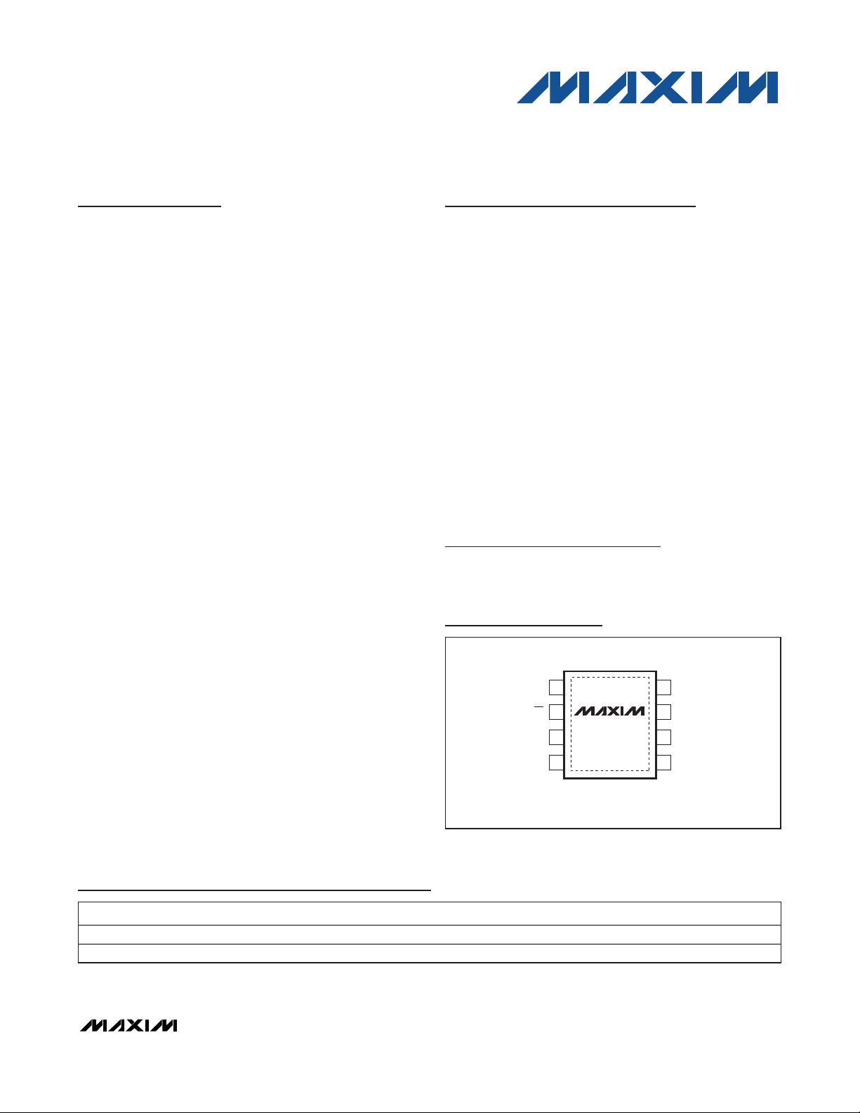
Pin Configurations
Pin Configurations continued at end of data sheet.
TOP VIEW
1
RO
+
87V
CC
2
MAX13410E
3
DE
4
MAX13411E
*EP
BRE
A
6
GNDDI
5
*EXPOSED PAD CONNECTED TO GROUND
SO
PART PIN-PACKAGE AutoDirection DATA RATE (max) 5V LDO OUTPUT
MAX13410EESA+ 8 SO-EP* No 500 kbps No
MAX13411EESA+ 8 SO-EP* No 16Mbps No
MAX13410E–MAX13415E
RS-485 Transceiver with Integrated Low-Dropout
Regulator and AutoDirection Control
2 _______________________________________________________________________________________
ABSOLUTE MAXIMUM RATINGS
Stresses beyond those listed under “Absolute Maximum Ratings” may cause permanent damage to the device. These are stress ratings only, and functional
operation of the device at these or any other conditions beyond those indicated in the operational sections of the specifications is not implied. Exposure to
absolute maximum rating conditions for extended periods may affect device reliability.
(All voltages referenced to GND.)
V
CC
.........................................................................-0.3V to +30V
RE, DE/RE, DE, DI, RO, V
REG
..................................-0.3V to +6V
A, B............................................................................-8V to +13V
Short-Circuit Duration (RO, A, B) to GND ................. Continuous
Continuous Power Dissipation (T
A
= +70°C)
8-Pin SO-EP (derate 19.2mW/°C above +70°C) ........1539mW
Operating Temperature Range ...........................-40°C to +85°C
Storage Temperature Range ............................-65°C to +150°C
Junction Temperature......................................................+150°C
θ
JA
(Note 1)...................................................................52.0°C/W
θ
JC
(Note 1).....................................................................6.0°C/W
Lead Temperature (soldering, 10s) ................................+300°C
Note 1: Package thermal resistances were obtained using the method described in JEDEC specificactions JESD51-7 using a four layer board.
For detailed information on package consitencies refer to www.maxim-ic/thermal-tutorial.
ELECTRICAL CHARACTERISTICS
(VCC= +6.0V to +28V, TA= T
MIN
to T
MAX
, unless otherwise noted. Typical values are at VCC= +7.5V, CS= 1µF, and TA= +25°C.) (Note 2)
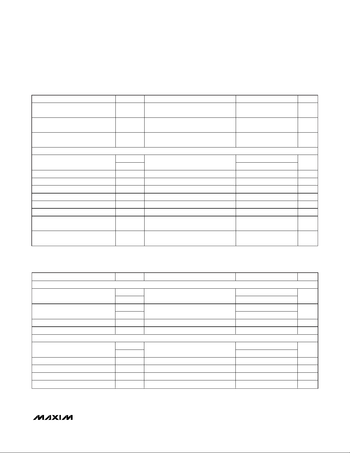
Supply Voltage V
LDO Output Voltage V
LDO Output Current I
LDO Dropout Voltage V
PARAMETER SYMBOL CONDITIONS MIN TYP MAX UNITS
Minimum Bypass Capacitor on V
Supply Current I
Shutdown Current I
Thermal-Shutdown Threshold T
Thermal-Shutdown Threshold
Hysteresis
DRIVER
Change in Magnitude of Differential
Output Voltage
Driver Common-Mode Output Voltage V
Change In Magnitude of CommonMode Voltage
Input High Voltage V
Input Low Voltage V
Input Current I
Driver-Disable Threshold V
(Note 3) 6.0 28.0 V
CC
VCC = +7.5V, I
VCC = +28V, I
VCC > +7.5V 20
VCC = +5V, I
DO
Guaranteed by design,
S
MAX13412E–MAX13415E
RE, DE = high/no load
(MAX13410E/MAX13411E)
CC
RE, DE/RE = high, DI = low/no load
(MAX13412E–MAX13415E)
DE = low, RE = high
(MAX13410E/MAX13411E)
TS
R
= 100Ω, Figure 1 2.0 5.5
DIFF
R
= 54Ω, Figure 1 1.5 5.5Differential Driver Output V
OD
OD
OC
OC
IH
IL
IN
DT
DIFF
No load 5.5
R
= 100Ω or 54Ω, Figure 1 0.2 V
DIFF
R
= 100Ω or 54Ω, Figure 1 1 3 V
DIFF
R
= 100Ω or 54Ω, Figure 1 0.2 V
DIFF
DI, DE, RE, DE/RE 2.0 V
DI, DE, RE, DE/RE 0.8 V
DI, DE, RE, DE/RE ±1 µA
TA = +25°C (MAX13412E/MAX13413E) 0.6 1.0 V
REG
REG
REG
C
SHDN
T
TSH
ΔV
ΔV
= 20mA 4.5 5 5.5
LOAD
= 0mA 4.5 5 5.5
LOAD
= 20mA 0.5 V
OUT
1µF
10
10
45 µA
+150 °C
15 °C
V
mA
mA
V
MAX13410E–MAX13415E
RS-485 Transceiver with Integrated Low-Dropout
Regulator and AutoDirection Control
_______________________________________________________________________________________ 3
SWITCHING CHARACTERISTICS–MAX13410E
(VCC= +6.0V to +28V, TA= T
MIN
to T
MAX
, unless otherwise noted. Typical values are at VCC= +7.5V, CS= 1µF, and TA= +25°C.) (Note 2)
)
)
ELECTRICAL CHARACTERISTICS (continued)
(VCC= +6.0V to +28V, TA= T
MIN
to T
MAX
, unless otherwise noted. Typical values are at VCC= +7.5V, CS= 1µF, and TA= +25°C.) (Note 2)
PARAMETER SYMBOL CONDITIONS MIN TYP MAX UNITS
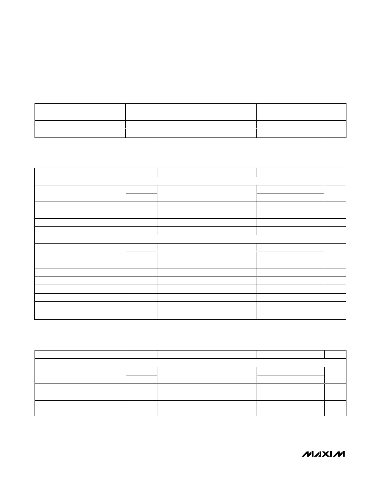
Driver Short-Circuit Output Current I
Driver Short-Circuit-Foldback Output
Current
RECEIVER
Input Current (A and B) I
Receiver Differential Threshold
Voltage
Receiver Input Hysteresis ΔV
Output High Voltage V
Output Low Voltage V
Thr ee- S tate O utp ut C ur r ent at Recei ver I
Receiver-Input Resistance R
Receiver-Output Short-Circuit Current I
ESD PROTECTION
ESD Protection (A, B)
ESD Protection (A, B)
ESD Protection (All Other Pins) Human Body Model ±2
OSD
I
OSDF
A, B
V
TH
OH
OL
OZR
OSR
0V < V
-7V < V
(VCC - 1V) < V
-7V < V
RE, DE, DE/RE =
GND, V
-7V < VCM < +12V
(MAX13410E/MAX13411E)
-7V < VLM < +12V
(MAX13412E/MAX13413E)
VA + VB = 0V 15 mV
TH
IO = -1mA, VA - VB > V
IO = +1mA, VA - VB < -V
0 < VO < V
-7V < VCM < +12V 96 kΩ
IN
0V < VRO < V
< +12V +250
OUT
< 0V -250
OUT
< +12V 20
OUT
< 0V -20
OUT
VIN = +12V 125
CC
= GND
V
= -7V -100
IN
-200 -50
-100 100
V
TH
TH
REG
REG
- 0.6 V
REG
±8 ±95
Human Body Model
(MAX13412E/MAX13413E)
Human Body Model
(MAX13410E/MAX13411E)
mA
mA
µA
mV
0.4 V
0.01 ±1 µA
mA
±15 kV
±14 kV
kV
PARAMETER SYMBOL CONDITIONS MIN TYP MAX UNITS
DRIVER
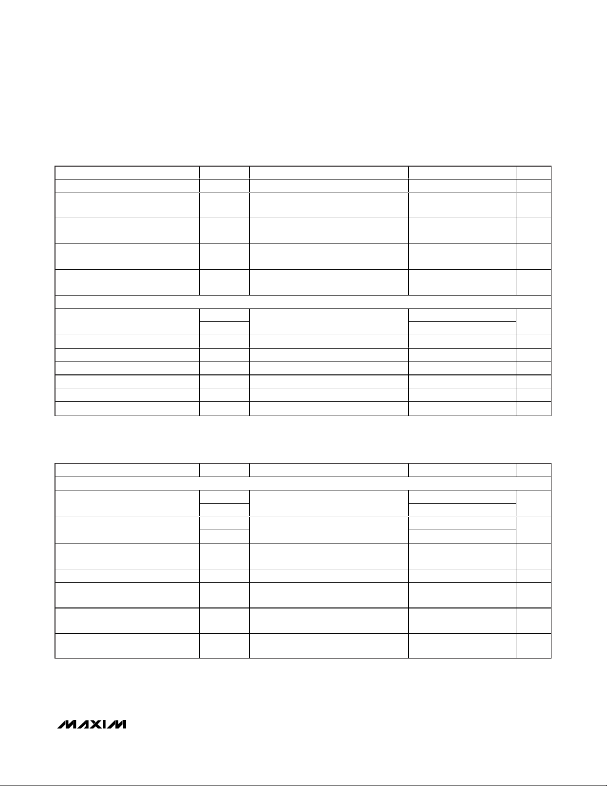
Driver Propagation Delay
Driver Differential Output
Rise or Fall Time
Driver Differential Output Skew
- t
|t
DPLH
DPHL
|
Maximum Data Rate f
Driver Enable from Shutdown to
Output High
Driver Enable from Shutdown to
Output Low
t
DPLH
t
DPHL
t
HL
t
LH
t
DSKEW
MAX
t
DZH(SHDN
t
DZL(SHDN
R
= 54Ω, CL = 50pF,
DIFF
Figures 2a and 3a
R
= 54Ω, CL = 50pF,
DIFF
Figures 2a and 3a
R
= 54Ω, CL = 50pF,
DIFF
Figures 2a and 3a
S2 closed, Figure 4,
R
= 500Ω, CL = 100pF
L
S2 closed, Figure 4,
R
= 500Ω, CL = 100pF
L
150 1000
150 1000
250 900
250 900
ns
ns
140 ns
500 kbps
11 µs
6µs
MAX13410E–MAX13415E
RS-485 Transceiver with Integrated Low-Dropout
Regulator and AutoDirection Control
4 _______________________________________________________________________________________
)
)
SWITCHING CHARACTERISTICS–MAX13411E
(VCC= +6.0V to +28V, TA= T
MIN
to T
MAX
, unless otherwise noted. Typical values are at VCC= +7.5V, CS= 1µF, and TA= +25°C.) (Note 2)
)
)
SWITCHING CHARACTERISTICS–MAX13410E (continued)
(VCC= +6.0V to +28V, TA= T
MIN
to T
MAX
, unless otherwise noted. Typical values are at VCC= +7.5V, CS= 1µF, and TA= +25°C.) (Note 2)
PARAMETER SYMBOL CONDITIONS MIN TYP MAX UNITS
Driver Enable to Output High t
Driver Enable to Output Low t
Driver Disable from Output High t
Driver Disable from Output Low t
Time to Shutdown t
RECEIVER
Receiver Propagation Delay
Receiver Output Skew t
Maximum Data Rate f
Receiver Enable to Output High t
Receiver Enable to Output Low t
Receiver Disable Time from High t
Receiver Disable Time from Low t
Receiver Enable from Shutdown to
Output High
Receiver Enable from Shutdown to
Output Low
DZH
DZL
DHZ
DLZ
SHDN
t
RPLH
t
RPHL
RSKEW
MAX
RZH
RZL
RZH
RLZ
t
RZH(SHDN
t
RZL(SHDN
S2 closed, Figure 4,
R
= 500Ω, CL = 100pF
L
S1 closed, Figure 4,
R
= 500Ω, CL = 100pF
L
S2 closed, Figure 4,
R
= 500Ω, CL = 100pF
L
S1 closed, Figure 4,
R
= 500Ω, CL = 100pF
L
50 340 700 ns
CL = 15pF (at RO), Figures 5 and 6
CL = 15pF (at RO), Figures 5 and 6 30 ns
500 kbps
S2 closed, Figure 7, CL = 15pF 50 ns
S1 closed, Figure 7, CL = 15pF 50 ns
S2 closed, Figure 7, CL = 15pF 50 ns
S1 closed, Figure 7, CL = 15pF 50 ns
S2 closed, Figure 7, CL = 15pF 14 µs
S1 closed, Figure 7, CL = 15pF 3.5 µs
2500 ns
2500 ns
100 ns
100 ns
200
200
ns
PARAMETER SYMBOL CONDITIONS MIN TYP MAX UNITS
DRIVER
Driver Propagation Delay
Driver Differential Output
Rise or Fall Time
Driver Differential Output Skew
- t
|t
DPLH
DPHL
|
Maximum Data Rate f
Driver Enable from Shutdown to
Output High
Driver Enable from Shutdown to
Output Low
Driver Enable to Output High t
t
DPLH
t
DPHL
t
HL
t
LH
t
DSKEW
MAX
t
DZH(SHDN
t
DZL(SHDN
DZH
R
= 54Ω, CL = 50pF, Figures 2a
DIFF
and 3a
R
= 54Ω, CL = 50pF, Figures 2a
DIFF
and 3a
R
= 54Ω, CL = 50pF, Figures 2a
DIFF
and 3a
S2 closed, Figure 4,
R
= 500Ω, CL = 100pF
L
S2 closed, Figure 4,
R
= 500Ω, CL = 100pF
L
S2 closed, Figure 4,
R
= 500Ω, CL = 100pF
L
16 Mbps
50
50
15
15
ns
ns
8ns
11 µs
6µs
70 ns
MAX13410E–MAX13415E
RS-485 Transceiver with Integrated Low-Dropout
Regulator and AutoDirection Control
_______________________________________________________________________________________ 5
SWITCHING CHARACTERISTICS–MAX13411E (continued)
(VCC= +6.0V to +28V, TA= T
MIN
to T
MAX
, unless otherwise noted. Typical values are at VCC= +7.5V, CS= 1µF, and TA= +25°C.) (Note 2)
)
)
SWITCHING CHARACTERISTICS–MAX13412E
(VCC= +6.0V to +28V, TA= T
MIN
to T
MAX
, unless otherwise noted. Typical values are at VCC= +7.5V, CS= 1µF, and TA= +25°C.) (Note 2)
PARAMETER SYMBOL CONDITIONS MIN TYP MAX UNITS
Driver Enable to Output Low t
Driver Disable from Output High t
Driver Disable from Output Low t
RECEIVER
Receiver Propagation Delay
Receiver Output Skew t
Maximum Data Rate f
Receiver Enable to Output High t
Receiver Enable to Output Low t
Receiver Disable Time from High t
Receiver Disable Time from Low t
Receiver Enable from Shutdown to
Output High
Receiver Enable from Shutdown to
Output Low
DZL
DHZ
DLZ
t
RPLH
t
RPHL
RSKEW
MAX
RZH
RZL
RZH
RLZ
t
RZH(SHDN
t
RZL(SHDN
S1 closed, Figure 4,
R
= 500Ω, CL = 100pF
L
S2 closed, Figure 4,
R
= 500Ω, CL = 100pF
L
S1 closed, Figure 4,
R
= 500Ω, CL = 100pF
L
CL = 15pF (at RO), Figures 5 and 6
CL = 15pF (at RO), Figures 5 and 6 8 ns
S2 closed, Figure 7, CL = 15pF 50 ns
S1 closed, Figure 7, CL = 15pF 50 ns
S2 closed, Figure 7 , CL = 15pF 50 ns
S1 closed, Figure 7, CL = 15pF 50 ns
S2 closed, Figure 7, CL = 15pF 14 µs
S1 closed, Figure 7, CL = 15pF 3.5 µs
70 ns
50 ns
50 ns
75
75
16 Mbps
ns
PARAMETER SYMBOL CONDITIONS MIN TYP MAX UNITS
DRIVER
Driver Propagation Delay
Driver Differential Output
Rise or Fall Time
Maximum Data Rate f
Driver Disable Delay t
RECEIVER
Receiver Propagation Delay
Receiver Output Skew t
Maximum Data Rate f
Receiver Enable to Output High t
Receiver Enable to Output Low t
t
DPLH
t
DPHL
t
HL
t
LH
MAX
DDD
t
RPLH
t
RPHL
RSKEW
MAX
RZH
RZL
RL = 110Ω, CL = 50pF, Figures 2b
and 3b
RL = 110Ω, CL = 50pF, Figures 2b
and 3b
RL = 110Ω, CL = 50pF, Figure 3b 2500 ns
CL = 15pF, Figures 5 and 6
CL = 15pF, Figures 5 and 6 30 ns
S2 closed, Figure 7, CL = 15pF 50 ns
S1 closed, Figure 7, CL = 15pF 50 ns
200 1000
200 1000
250 900
250 900
500 kbps
200
200
500 kbps
ns
ns
ns
MAX13410E–MAX13415E
RS-485 Transceiver with Integrated Low-Dropout
Regulator and AutoDirection Control
6 _______________________________________________________________________________________
SWITCHING CHARACTERISTICS–MAX13412E (continued)
(VCC= +6.0V to +28V, TA= T
MIN
to T
MAX
, unless otherwise noted. Typical values are at VCC= +7.5V, CS= 1µF, and TA= +25°C.) (Note 2)
SWITCHING CHARACTERISTICS–MAX13413E
(VCC= +6.0V to +28V, TA= T
MIN
to T
MAX
, unless otherwise noted. Typical values are at VCC= +7.5V, CS= 1µF, and TA= +25°C.) (Note 2)
SWITCHING CHARACTERISTICS–MAX13414E
(VCC= +6.0V to +28V, TA= T
MIN
to T
MAX
, unless otherwise noted. Typical values are at VCC= +7.5V, CS= 1µF, and TA= +25°C.) (Note 2)
PARAMETER SYMBOL CONDITIONS MIN TYP MAX UNITS
Receiver Disable Time from Low t
Receiver Disable Time from High t
Receiver Enable Delay t
PARAMETER SYMBOL CONDITIONS MIN TYP MAX UNITS
DRIVER
Driver Propagation Delay
Driver Differential Output
Rise or Fall Time
Maximum Data Rate f
Driver Disable Delay t
RECEIVER
Receiver Propagation Delay
Receiver Output Skew t
Maximum Data Rate f
Receiver Enable to Output High t
Receiver Enable to Output Low t
Receiver Disable Time from Low t
Receiver Disable Time from High t
Receiver Enable Delay t
RLZ
RZH
RED
t
DPLH
t
DPHL
t
HL
t
LH
MAX
DDD
t
RPLH
t
RPHL
RSKEW
MAX
RZH
RZL
RLZ
RZH
RED
S1 closed, Figure 7, CL = 15pF 50 ns
S2 closed, Figure 7, CL = 15pF 50 ns
RL = 110Ω, CL = 50pF, Figure 3 2500 ns
RL = 110Ω, CL = 50pF, Figures 2b
and 3b
RL = 110Ω, CL = 50pF, Figures 2b
and 3b
16 Mbps
RL = 110Ω, CL = 50pF, Figure 3b 70 ns
CL = 15pF, Figures 5 and 6
CL = 15pF, Figures 5 and 6 13 ns
16 Mbps
S2 closed, Figure 7, CL = 15pF 50 ns
S1 closed, Figure 7, CL = 15pF 50 ns
S1 closed, Figure 7, CL = 15pF 50 ns
S2 closed, Figure 7, CL = 15pF 50 ns
RL = 110Ω, Figure 3, CL = 50pF 70 ns
50
50
15
15
80
80
ns
ns
ns
PARAMETER SYMBOL CONDITIONS MIN TYP MAX UNITS
DRIVER
Driver Propagation Delay
Driver Differential Output
Rise or Fall Time
Driver Differential Output Skew
|t
- t
DPHL
|
DPLH
t
DPLH
t
DPHL
t
HL
t
LH
t
DSKEW
R
= 54Ω, CL = 50pF, Figures 2a
DIFF
and 3a
R
= 54Ω, CL = 50pF, Figures 2a
DIFF
and 3a
R
= 54Ω, CL = 50pF, Figures 2a
DIFF
and 3a
200 1000
200 1000
250 900
250 900
ns
ns
140 ns
MAX13410E–MAX13415E
RS-485 Transceiver with Integrated Low-Dropout
Regulator and AutoDirection Control
_______________________________________________________________________________________ 7
SWITCHING CHARACTERISTICS–MAX13414E (continued)
(VCC= +6.0V to +28V, TA= T
MIN
to T
MAX
, unless otherwise noted. Typical values are at VCC= +7.5V, CS= 1µF, and TA= +25°C.) (Note 2)
SWITCHING CHARACTERISTICS–MAX13415E
(VCC= +6.0V to +28V, TA= T
MIN
to T
MAX
, unless otherwise noted. Typical values are at VCC= +7.5V, CS= 1µF, and TA= +25°C.) (Note 2)
PARAMETER SYMBOL CONDITIONS MIN TYP MAX UNITS
Maximum Data Rate f
Driver Enable to Output High t
Driver Enable to Output Low t
Driver Disable from Output High t
Driver Disable from Output Low t
RECEIVER
Receiver Propagation Delay
Receiver Output Skew t
Maximum Data Rate f
Receiver Enable to Output High t
Receiver Enable to Output Low t
Receiver Disable Time from Low t
Receiver Disable Time from High t
MAX
DZH
DZL
DHZ
DLZ
t
RPLH
t
RPHL
RSKEW
MAX
RZH
RZL
RLZ
RZH
S2 closed, Figure 4,
= 500Ω CL = 100pF
R
L
S1 closed, Figure 4,
= 500Ω CL = 100pF
R
L
S2 closed, Figure 4,
= 500Ω, CL = 100pF
R
L
S1 closed, Figure 4,
= 500Ω, CL = 100pF
R
L
CL = 15pF (at RO), Figures 5 and 6
CL = 15pF (at RO), Figures 5 and 6 30 ns
S2 closed, Figure 7, CL = 15pF 50 ns
S1 closed, Figure 7, CL = 15pF 50 ns
S1 closed, Figure 7, CL = 15pF 50 ns
S2 closed, Figure 7, CL = 15pF 50 ns
500 kbps
2500 ns
2500 ns
100 ns
100 ns
200
200
ns
500 kbps
PARAMETER SYMBOL CONDITIONS MIN TYP MAX UNITS
DRIVER
Driver Propagation Delay
Driver Differential Output
Rise or Fall Time
Driver Differential Output Skew
|t
- t
DPHL
|
DPLH
Maximum Data Rate f
Driver Enable to Output High t
Driver Enable to Output Low t
Driver Disable from Output High t
t
DPLH
t
DPHL
t
HL
t
LH
t
DSKEW
MAX
DZH
DZL
DHZ
R
= 54Ω, CL = 50pF, Figures 2a
DIFF
and 3a
R
= 54Ω, CL = 50pF, Figures 2a
DIFF
and 3a
R
= 54Ω, CL = 50pF, Figures 2a
DIFF
and 3a
S2 closed, Figure 4,
= 500Ω, CL = 15pF
R
L
S1 closed, Figure 4,
= 500Ω, CL = 15pF
R
L
S2 closed, Figure 4,
= 500Ω, CL = 15pF
R
L
50
50
15
15
ns
ns
8ns
16 Mbps
70 ns
70 ns
50 ns
MAX13410E–MAX13415E
RS-485 Transceiver with Integrated Low-Dropout
Regulator and AutoDirection Control
8 _______________________________________________________________________________________
SWITCHING CHARACTERISTICS–MAX13415E (continued)
(VCC= +6.0V to +28V, TA= T
MIN
to T
MAX
, unless otherwise noted. Typical values are at VCC= +7.5V, CS= 1µF, and TA= +25°C.) (Note 2)
Note 2: CSis the compensation capacitor on V
REG
for the MAX13412E–MAX13415E versions. CSmust have an ESR value of 20mΩ or less.
Note 3: Parameters are guaranteed for +6.0V ≤ V
CC
≤ +28V.
Typical Operating Characteristics
(VCC= +7.5V, TA= +25°C, unless otherwise noted.)
PARAMETER SYMBOL CONDITIONS MIN TYP MAX UNITS
Driver Disable from Output Low t
RECEIVER
Receiver Propagation Delay
Receiver Output Skew t
Maximum Data Rate f
Receiver Enable to Output High t
Receiver Enable to Output Low t
Receiver Disable Time from Low t
Receiver Disable Time from High t
DLZ
t
RPLH
t
RPHL
RSKEW
MAX
RZH
RZL
RLZ
RZH
S1 closed, Figure 4,
= 500Ω, CL = 15pF
R
L
CL = 15pF (at RO), Figures 5 and 6
CL = 15pF (at RO), Figures 5 and 6 8 ns
16 Mbps
S2 closed, Figure 7, CL = 15pF 50 ns
S1 closed, Figure 7, CL = 15pF 50 ns
S1 closed, Figure 7, CL = 15pF 50 ns
S2 closed, Figure 7, CL = 15pF 50 ns
50 ns
75
75
ns
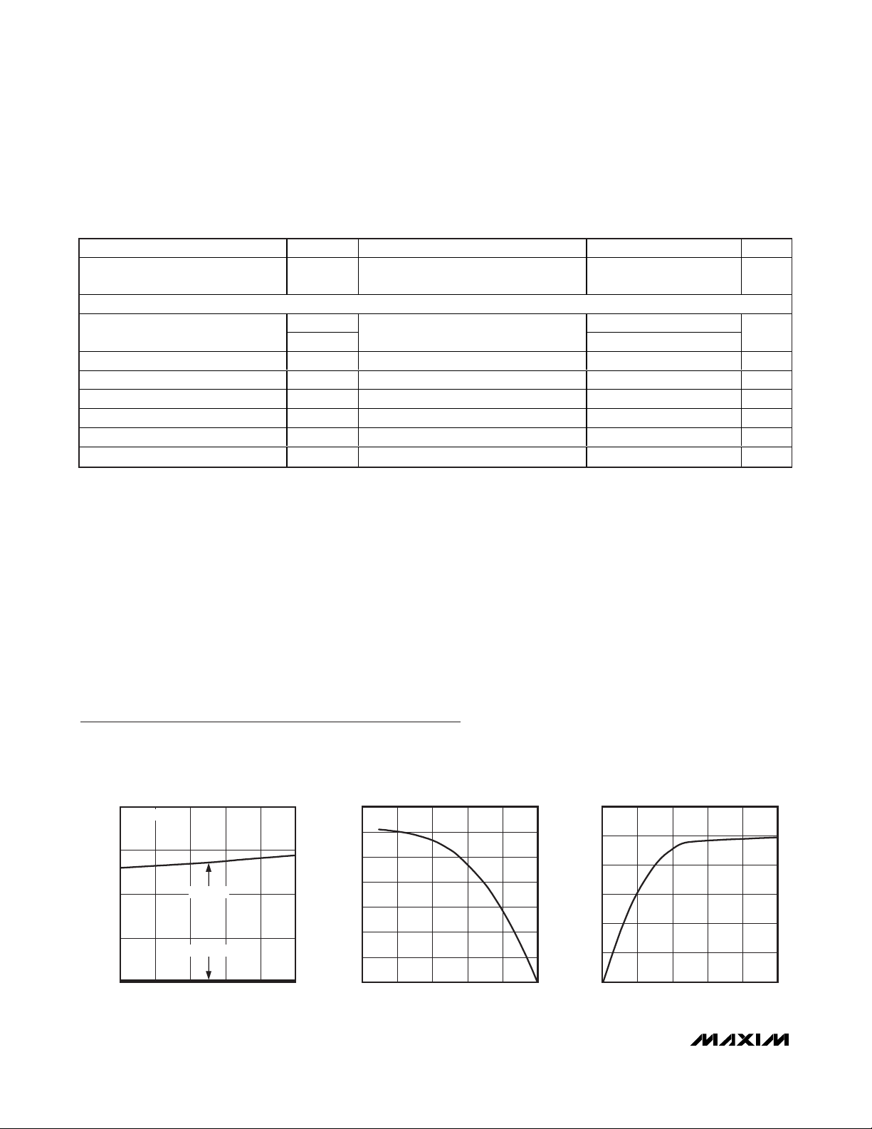
SUPPLY CURRENT
vs. TEMPERATURE
8.0
NO LOAD
6.0
4.0
SUPPLY CURRENT (mA)
2.0
DE = HIGH
DE = LOW
MAX13410E-15E toc01
OUTPUT CURRENT (mA)
vs. RECEIVER OUTPUT HIGH VOLTAGE
35
30
25
20
15
10
5
OUTPUT CURRENT
OUTPUT CURRENT
60
50
MAX13410E-15E toc02
40
30
20
OUTPUT CURRENT (mA)
10
vs. RECEIVER OUTPUT LOW VOLTAGE
MAX13410E-15E toc03
0
-40 10-15 35 60 85
TEMPERATURE (°C)
0
021345
OUTPUT HIGH VOLTAGE (V)
0
05
OUTPUT LOW VOLTAGE (V)
2134
 Loading...