

General Description
The MAX1334/MAX1335 2-channel, serial-output,
10-bit, analog-to-digital converters (ADCs) feature two
true-differential analog inputs and offer outstanding noise
immunity and dynamic performance. Both devices easily
interface with SPI™/QSPI™/MICROWIRE™ and standard
digital signal processors (DSPs).
The MAX1334 operates from a single +4.75V to +5.25V
supply with sampling rates up to 4.5Msps. The
MAX1335 operates from a single +2.7V to +3.6V supply
with sampling rates up to 4Msps. These devices feature
a partial power-down mode and a full power-down
mode that reduce the supply current to 3.3mA and
0.2µA, respectively. Also featured is a separate powersupply input (DVDD) that allows direct interfacing to
+2.7V to +3.6V digital logic. The fast conversion speed,
low power dissipation, excellent AC performance, and
DC accuracy (±0.4 LSB INL) make the MAX1334/
MAX1335 ideal for industrial process control, motor
control, and base-station applications.
The MAX1334/MAX1335 are available in a space-saving (3mm x 3mm), 16-pin, TQFN package and operate
over the extended (-40°C to +85°C) temperature range.
Applications
Data Acquisition
Bill Validation
Motor Control
Base Stations
High-Speed Modems
Optical Sensors
Industrial Process Control
Features
♦ 4.5Msps Sampling Rate (+5V, MAX1334)
♦ 4Msps Sampling Rate (+3V, MAX1335)
♦ Separate Logic Supply: +2.7V to +3.6V
♦ Two True-Differential Analog Input Channels
♦ Bipolar/Unipolar Selection Input
♦ Only 40mW (typ) Power Consumption
♦ Only 2µA (max) Shutdown Current
♦ High-Speed, SPI-Compatible, 3-Wire Serial
Interface
♦ 2.6MHz Full-Linear Bandwidth
♦ 61dB SINAD at 525kHz Input Frequency
♦ No Pipeline Delays
♦ Space-Saving (3mm x 3mm), 16-Pin TQFN
Package
MAX1334/MAX1335
4.5Msps/4Msps, 5V/3V, 2-Channel,
True-Differential, 10-Bit ADCs
________________________________________________________________ Maxim Integrated Products 1
Ordering Information
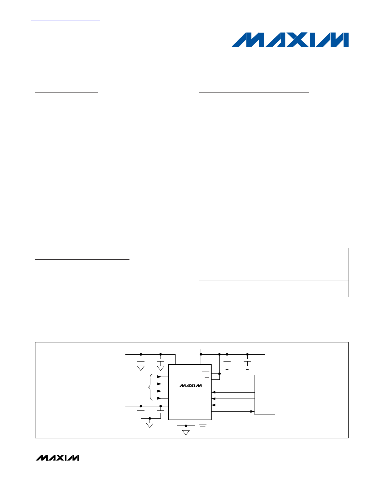
AIN1P
DOUT
SCLK
CNVST
AIN1N
REF
DIFFERENTIAL
INPUT VOLTAGE
+4.75V TO +5.25V
+2.7V TO +3.6V
µC/DSP
CHSEL
+
-
AV
DD
DV
DD
AGND AGND DGND
BIP/UNI
SHDN
0.01µF0.01µF1µF
1µF
0.01µF
1µF
AIN0P
AIN0N
REF INPUT
VOLTAGE
+
-
MAX1334
Typical Operating Circuit
19-3767; Rev 1; 10/05
For pricing, delivery, and ordering information, please contact Maxim/Dallas Direct! at
1-888-629-4642, or visit Maxim’s website at www.maxim-ic.com.
SPI/QSPI are trademarks of Motorola, Inc.
MICROWIRE is a trademark of National Semiconductor Corp.
*EP = Exposed paddle.
**Future product—contact factory for availability.
Selector Guide appears at end of data sheet.
Pin Configuration appears at end of data sheet.
查询MAX1329供应商
PART TEMP RANGE PIN-PACKAGE
MAX1334ETE** -40°C to +85°C
MAX1335ETE -40°C to +85°C
16 TQFN-EP*
(3mm x 3mm)
16 TQFN-EP*
(3mm x 3mm)
T1633F-3
T1633F-3
PKG
CODE
MAX1334/MAX1335
4.5Msps/4Msps, 5V/3V, 2-Channel,
True-Differential, 10-Bit ADCs
2 _______________________________________________________________________________________
ABSOLUTE MAXIMUM RATINGS
Stresses beyond those listed under “Absolute Maximum Ratings” may cause permanent damage to the device. These are stress ratings only, and functional
operation of the device at these or any other conditions beyond those indicated in the operational sections of the specifications is not implied. Exposure to
absolute maximum rating conditions for extended periods may affect device reliability.
AVDDto AGND (MAX1334) ......................................-0.3V to +6V
AV
DD
to AGND (MAX1335) ......................................-0.3V to +4V
DV
DD
to DGND.........................................................-0.3V to +4V
AGND to DGND.....................................................-0.3V to +0.3V
SCLK, CNVST, SHDN, CHSEL, BIP/UNI,
DOUT to DGND ...................................-0.3V to (DV
DD
+ 0.3V)
AIN0P, AIN0N, AIN1P, AIN1N, REF to
AGND...................................................-0.3V to (AV
DD
+ 0.3V)
Maximum Current into Any Pin .........................................±50mA
Continuous Power Dissipation (T
A
= +70°C)
16-Pin TQFN (derate 17.5mW/°C above +70°C) ....1398.6mW
Operating Temperature Range ...........................-40°C to +85°C
Junction Temperature......................................................+150°C
Storage Temperature Range .............................-60°C to +150°C
Lead Temperature (soldering, 10s) .................................+300°C
ELECTRICAL CHARACTERISTICS (MAX1334)
(AVDD= +4.75V to +5.25V, DVDD= +2.7V to +3.6V, f
SCLK
= 76MHz, V
REF
= 4.096V, TA= T
MIN
to T
MAX
, unless otherwise noted.
Typical values are at T
A
= +25°C.)
PARAMETER SYMBOL CONDITIONS MIN TYP MAX UNITS
DC ACCURACY (Note 1) (BIP/UNI = DGND)
Resolution N 10 Bits
Integral Nonlinearity INL ±0.4 ±1.0 LSB
Differential Nonlinearity DNL ±0.4 ±1.0 LSB
Offset Error ±1.0 ±1.5 LSB
Gain Error ±1.5 ±4.0 LSB
Offset-Error Temperature
Coefficient
Gain-Error Temperature
Coefficient
DYNAMIC SPECIFICATIONS (AIN = -0.2dBFS, fIN = 525kHz, BIP/UNI = DVDD, unless otherwise noted) (Note 1)
Signal-to-Noise Ratio SNR 66 61 dB
Signal-to-Noise Plus Distortion SINAD 59.5 61 dB
Total Harmonic Distortion THD -77 -68 dBc
Spurious-Free Dynamic Range SFDR 68 78 dBc
Intermodulation Distortion IMD
Channel-to-Channel Isolation 76 dB
Full-Linear Bandwidth SINAD > 56dB 2.6 MHz
Full-Power Bandwidth 5.4 MHz
Small-Signal Bandwidth 5MHz
CONVERSION RATE
Minimum Conversion Time t
Maximum Throughput Rate 4.5 Msps
Minimum Track-and-Hold
Acquisition Time
CONV
t
ACQ
f
IN1
f
IN2
Figure 5 171 ns
Figure 5 32 ns
= 103.5kHz, A
= 113.5kHz, A
= TBDdBFS
IN1
= TBDdBFS
IN2
±1.1 ppm/°C
±4.5 ppm/°C
-72 dB
MAX1334/MAX1335
4.5Msps/4Msps, 5V/3V, 2-Channel,
True-Differential, 10-Bit ADCs
_______________________________________________________________________________________ 3
ELECTRICAL CHARACTERISTICS (MAX1334) (continued)
(AVDD= +4.75V to +5.25V, DVDD= +2.7V to +3.6V, f
SCLK
= 76MHz, V
REF
= 4.096V, TA= T
MIN
to T
MAX
, unless otherwise noted.
Typical values are at T
A
= +25°C.)
PARAMETER SYMBOL CONDITIONS MIN TYP MAX UNITS
Aperture Delay t
Aperture Jitter t
AD
AJ
Figure 21 < 10 ns
Figure 21 < 10 ps
DIFFERENTIAL ANALOG INPUTS (AIN0P, AIN0N, AIN1P, AIN1N)
Differential Input Voltage Range
(V
AIN_P
- V
AIN_N
)
V
BIP/UNI = DGND 0 V
IN
BIP/UNI = DV
Absolute Input Voltage Range
DC Leakage Current I
Input Capacitance C
LKG
IN
REFERENCE INPUT (REF)
REF Input Voltage Range V
REF Input Capacitance C
REF DC Leakage Current I
REF
REF
REF
DIGITAL INPUTS (SCLK, CNVST, SHDN, CHSEL, BIP/UNI)
Input-Voltage Low V
Input-Voltage High V
IL
IH
Input Hysteresis 100 mV
Input Leakage Current I
Input Capacitance C
ILKG
IN
DIGITAL OUTPUT (DOUT)
Output-Voltage Low V
Output-Voltage High V
Tri-State Leakage Current I
Tri-State Output Capacitance C
OL
OH
LKGT
OUT
I
SINK
I
SOURCE
Between conversions, CNVST = DV
Between conversions, CNVST = DV
POWER REQUIREMENTS
Analog Supply Voltage AV
Digital Supply Voltage DV
DD
DD
Normal mode; average unloaded current
(f
Analog Supply Current I
AVDD
SAMPLE
Partial power-down mode 3.3 4
Full power-down mode 0.1 2 µA
DD
-V
REF
AGND
- 50mV
/ 2 +V
REF
/ 2
REF
AV
DD
+
50mV
±10 µA
14 pF
AV
DD
1.0
+
50mV
14 pF
±10 µA
0.3 x
DV
DD
0.7 x
DV
DD
±0.2 ±5 µA
15 pF
= 5mA 0.4 V
DV
-
= 1mA
DD
DD
DD
0.5
±1 µA
15 pF
4.75 5.25 V
2.7 3.6 V
= 4.0MHz, f
SCLK
= 64MHz)
11 12
V
V
V
V
V
V
mA
MAX1334/MAX1335
4.5Msps/4Msps, 5V/3V, 2-Channel,
True-Differential, 10-Bit ADCs
4 _______________________________________________________________________________________
ELECTRICAL CHARACTERISTICS (MAX1334) (continued)
(AVDD= +4.75V to +5.25V, DVDD= +2.7V to +3.6V, f
SCLK
= 76MHz, V
REF
= 4.096V, TA= T
MIN
to T
MAX
, unless otherwise noted.
Typical values are at T
A
= +25°C.)
TIMING CHARACTERISTICS (MAX1334) (Figure 4)
(AVDD= +4.75V to +5.25V, DVDD= +2.7V to +3.6V, TA= T
MIN
to T
MAX
, unless otherwise noted. Typical values are at TA= +25°C.)
Note 1: Tested with AVDD= 4.75V and DVDD= +2.7V.
Note 2: Guaranteed by design, not production tested.
PARAMETER SYMBOL CONDITIONS MIN TYP MAX UNITS
Power-Supply Rejection PSR AVDD = 4.75V to 5.25V, full-scale input ±0.5 ±0.3 mV
DVDD
Average unloaded current (f
4.5MHz, f
Power-down (f
Static or power-down, all digital inputs are
connected to DV
PARAMETER SYMBOL CONDITIONS MIN TYP MAX UNITS
SCLK Clock Period t
SCLK Pulse Width t
CNVST Rise to DOUT Disable t
CNVST Fall to DOUT Enable t
CHSEL to CNVST Fall Setup t
BIP/UNI to CNVST Fall Setup t
CNVST Fall to CHSEL Hold t
CNVST Fall to BIP/UNI Hold t
DOUT Remains Valid After SCLK t
SCLK Rise to DOUT Transition t
CNVST to SCLK Rise t
SCLK Rise to CNVST t
CNVST Pulse Width t
Minimum Recovery Time (Full
Power-Down)
Minimum Recovery Time (Partial
Power-Down)
CP
SPW
CRDD
CFDE
CHCF
BUCF
CFCH
CFBU
DHOLD
DOT
SETUP
HOLD
CSW
t
FPD
t
PPD
C
LOAD
C
LOAD
From CNVST fall or SHDN rise 4 µs
From CNVST fall 500 ns
= 76MHz, zero-scale input)
SCLK
= 76MHz) 18 45Digital Supply Current I
SCLK
DD
= 0pF (Note 2) 1 2 ns
= 30pF 6 ns
=
SAMPLE
or DGND
13.1 ns
6ns
15 ns
15 ns
32 ns
32 ns
0ns
0ns
6ns
0ns
6ns
58mA
0.2 2
µA
MAX1334/MAX1335
4.5Msps/4Msps, 5V/3V, 2-Channel,
True-Differential, 10-Bit ADCs
_______________________________________________________________________________________ 5
ELECTRICAL CHARACTERISTICS (MAX1335)
(AVDD= +2.7V to +3.6V, DVDD= +2.7V to +3.6V, f
SCLK
= 64MHz, V
REF
= 2.5V, TA= T
MIN
to T
MAX
, unless otherwise noted. Typical
values are at T
A
= +25°C.)
DC ACCURACY (Note 3) (BIP/UNI = DGND)
Resolution N 10 Bits
Relative Accuracy INL ±0.4 ±1.0 LSB
Differential Nonlinearity DNL ±0.4 ±1.0 LSB
Offset Error ±1.0 ±1.5 LSB
Gain Error ±1.5 ±4.0 LSB
Offset-Error Temperature
Coefficient
Gain-Error Temperature
Coefficient
DYNAMIC SPECIFICATIONS (AIN = -0.2dBFS, fIN = 525kHz, BIP/UNI = DVDD, unless otherwise noted) (Note 3)
Signal-to-Noise Ratio SNR 60 61 dB
Signal-to-Noise Plus Distortion SINAD 59.5 61 dB
Total Harmonic Distortion THD -77 -68 dBc
Spurious-Free Dynamic Range SFDR 68 78 dBc
Channel-to-Channel Isolation 76 dB
Full-Linear Bandwidth SINAD > 56dB 2.6 MHz
Full-Power Bandwidth 5.4 MHz
Small-Signal Bandwidth 5MHz
CONVERSION RATE
Minimum Conversion Time t
Maximum Throughput Rate 4 Msps
Minimum Track-and-Hold
Acquisition Time
Aperture Delay t
Aperture Jitter t
DIFFERENTIAL ANALOG INPUTS (AIN0P, AIN0N, AIN1P, AIN1N)
Differential Input Voltage Range
(V
AIN_P
Absolute Input Voltage Range
DC Leakage Current I
PARAMETER SYMBOL CONDITIONS MIN TYP MAX UNITS
CONV
t
ACQ
AD
AJ
V
- V
AIN_N
)
IN
LKG
Figure 5 203 ns
Figure 5 39 ns
Figure 21 < 10 ns
Figure 21 < 10 ps
BIP/UNI = DGND 0 V
BIP/ UNI = DV
DD
±1.1 ppm/°C
±4.5 ppm/°C
-V
/ 2 +V
REF
AGND
- 50mV
REF
/ 2
REF
AV
DD
+
50mV
±1 µA
V
V
MAX1334/MAX1335
4.5Msps/4Msps, 5V/3V, 2-Channel,
True-Differential, 10-Bit ADCs
6 _______________________________________________________________________________________
ELECTRICAL CHARACTERISTICS (MAX1335) (continued)
(AVDD= +2.7V to +3.6V, DVDD= +2.7V to +3.6V, f
SCLK
= 64MHz, V
REF
= 2.5V, TA= T
MIN
to T
MAX
, unless otherwise noted. Typical
values are at T
A
= +25°C.)
PARAMETER SYMBOL CONDITIONS MIN TYP MAX UNITS
Input Capacitance C
IN
REFERENCE INPUT (REF)
REF Input Voltage V
REF Input Capacitance C
REF DC Leakage Current I
REF
REF
REF
DIGITAL INPUTS (SCLK, CNVST, SHDN, CHSEL, BIP/UNI)
Input-Voltage Low V
Input-Voltage High V
IL
IH
Input Hysteresis 100 mV
Input Leakage Current I
Input Capacitance C
DIGITAL OUTPUT (DOUT)
Output-Voltage Low V
Output-Voltage High V
Tri-State Leakage Current I
Tri-State Output Capacitance C
POWER REQUIREMENTS
Analog Supply Voltage AV
Digital Supply Voltage DV
Analog Supply Current I
Positive Supply Rejection PSR AVDD = 2.7V to 3.6V, full-scale input ±6 mV
ILKG
IN
OL
OH
LKGT
OUT
DD
DD
AVDD
DVDD
14 pF
AV
1.0
50mV
14 pF
0.3 x
DV
0.7 x
DV
DD
±0.2 ±5 µA
15 pF
I
= 5mA 0.4 V
SINK
DV
-
I
SOURCE
= 1mA
Between conversions, CNVST = DV
Between conversions, CNVST = DV
DD
DD
DD
0.5
15 pF
2.7 3.6 V
2.7 AV
Normal mode; average unloaded current
(f
SAMPLE
= 4MHz, f
SCLK
= 64MHz)
9.6 12
Partial power-down mode 3.3 4
Full power-down mode 0.1 2 µA
Average unloaded current (f
4MHz, f
Power-down (f
= 64MHz, zero-scale input)
SCLK
= 40MHz) 18 45Digital Supply Current I
SCLK
Static or power-down; all digital inputs are
connected to DV
or DGND
DD
SAMPLE
=
5.0 8.0 mA
0.2 2
DD
+
±10 µA
DD
±1 µA
DD
mA
µA
V
V
V
V
V
MAX1334/MAX1335
4.5Msps/4Msps, 5V/3V, 2-Channel,
True-Differential, 10-Bit ADCs
_______________________________________________________________________________________ 7
TIMING CHARACTERISTICS (MAX1335) (Figure 4)
(AVDD= +2.7V to +3.6V, DVDD= +2.7V to +3.6V, TA= T
MIN
to T
MAX
, unless otherwise noted. Typical values are at TA= +25°C.)
Note 3: Tested with AVDD= DVDD= +2.7V.
Note 4: Guaranteed by design, not production tested.
Figure 1. Load Circuits for Enable/Disable Times
PARAMETER SYMBOL CONDITIONS MIN TYP MAX UNITS
SCLK Clock Period t
SCLK Pulse Width t
CNVST Rise to DOUT Disable t
CNVST Fall to DOUT Enable t
CHSEL to CNVST Fall Setup t
BIP/UNI to CNVST Fall Setup t
CNVST Fall to CHSEL Hold t
CNVST Fall to BIP/UNI Hold t
DOUT Remains Valid After SCLK t
SCLK Rise to DOUT Transition t
CNVST to SCLK Rise t
SCLK Rise to CNVST t
CNVST Pulse Width t
Minimum Recovery Time (Full
Power-Down)
Minimum Recovery Time (Partial
Power-Down)
CP
CPW
CRDD
CFDE
CHCF
BUCF
CFCH
CFBU
DHOLD
DOT
SETUP
HOLD
CSW
t
FPD
t
PPD
C
LOAD
C
LOAD
From CNVST fall or SHDN rise 4 µs
From CNVST fall 500 ns
= 0pF (Note 4) 1 2 ns
= 30pF 6 ns
15.6 ns
6ns
15 ns
15 ns
36 ns
36 ns
0ns
0ns
6ns
0ns
6ns
DOUT DOUT
6kΩ
a) HIGH IMPEDANCE TO VOH, V
AND V
TO HIGH IMPEDANCE
OH
30pF 30pF
DGND
TO VOH,
OL
DV
DD
6kΩ
DGND
b) HIGH IMPEDANCE TO V
AND V
TO HIGH IMPEDANCE
OL
OL, VOH
TO VOL,

MAX1334/MAX1335
4.5Msps/4Msps, 5V/3V, 2-Channel,
True-Differential, 10-Bit ADCs
8 _______________________________________________________________________________________
Typical Operating Characteristics
(AVDD= +3V, DVDD= +3V, V
REF
= 2.048V, f
SCLK
= 40MHz, TA= +25°C, unless otherwise noted.)
MAX1335
-1.0
-0.6
-0.8
-0.2
-0.4
0.2
0
0.4
0.8
0.6
1.0
0 256 384128 512 640 768 896 1024
INTEGRAL NONLINEARITY
vs. OUTPUT CODE
MAX1335 toc01
OUTPUT CODE
INL (LSB)
-1.0
-0.6
-0.8
-0.2
-0.4
0.2
0
0.4
0.8
1.0
0 256 384128 512 640 768 896 1024
DIFFERENTIAL NONLINEARITY
vs. OUTPUT CODE
MAX1335 toc02
OUTPUT CODE
INL (LSB)
0.6
-2.0
-1.5
-1.0
-0.5
0
0.5
1.0
1.5
2.0
-40 -15 10 35 60 85
OFFSET ERROR vs. TEMPERATURE
MAX1335 toc03
TEMPERATURE (°C)
OFFSET ERROR (LSB)
3.53.43.2 3.32.9 3.0 3.12.8
-1.5
-1.0
-0.5
0
0.5
1.0
1.5
2.0
-2.0
2.7 3.6
OFFSET ERROR
vs. AV
DD
SUPPLY VOLTAGE
MAX1335 toc04
OFFSET ERROR (LSB)
DVDD = AV
DD
AVDD (V)
-2.0
-1.5
-1.0
-0.5
0
0.5
1.0
1.5
2.0
-40 -15 10 35 60 85
GAIN ERROR vs. TEMPERATURE
MAX1335 toc05
TEMPERATURE (°C)
GAIN ERROR (LSB)
3.53.42.8 2.9 3.0 3.23.1 3.32.7 3.6
GAIN ERROR vs. AVDD SUPPLY VOLTAGE
MAX1335 toc06
AVDD (V)
GAIN ERROR (LSB)
-1.5
-1.0
-0.5
0
0.5
1.0
1.5
2.0
-2.0
DVDD = AV
DD
AVDD SUPPLY CURRENT vs. TEMPERATURE
MAX1335 toc07
TEMPERATURE (°C)
I
AV
DD
(mA)
603510-15
8.5
9.0
9.5
10.0
10.5
11.0
11.5
12.0
8.0
-40 85
AVDD SUPPLY CURRENT
vs. SCLK FREQUENCY
MAX1335 toc08
f
SCLK
(MHz)
I
AV
DD
(mA)
605010 20 30 40
8.5
9.0
9.5
10.0
10.5
11.0
11.5
12.0
8.0
070
8.5
9.0
9.5
10.0
10.5
11.0
11.5
12.0
8.0
MAX1335 toc09
AVDD (V)
DVDD = AV
DD
AVDD SUPPLY CURRENT
vs. AV
DD
SUPPLY VOLTAGE
I
AV
DD
(mA)
3.53.42.8 2.9 3.0 3.23.1 3.32.7 3.6

MAX1334/MAX1335
4.5Msps/4Msps, 5V/3V, 2-Channel,
True-Differential, 10-Bit ADCs
_______________________________________________________________________________________ 9
Typical Operating Characteristics (continued)
(AVDD= +3V, DVDD= +3V, V
REF
= 2.048V, f
SCLK
= 40MHz, TA= +25°C, unless otherwise noted.)
MAX1335
3.5
4.0
4.5
5.0
5.5
6.0
6.5
7.0
3.0
DVDD SUPPLY CURRENT vs. TEMPERATURE
MAX1335 toc10
TEMPERATURE (°C)
I
DV
DD
(mA)
603510-15-40 85
ZERO-SCALE INPUT
30
10 20
1
2
3
4
5
6
0
040
DVDD SUPPLY CURRENT
vs. SCLK FREQUENCY
MAX1335 toc11
f
SCLK
(MHz)
I
DV
DD
(mA)
50
60
70
3.23.12.8 2.9 3.0
3.5
4.0
4.5
5.0
5.5
6.0
6.5
7.0
3.0
2.7 3.3
MAX1335 toc12
DVDD (V)
DVDD SUPPLY CURRENT
vs. DV
DD
SUPPLY VOLTAGE
I
DV
DD
(mA)
3.63.5
3.4
AVDD = DV
DD
ZERO-SCALE INPUT
50
54
52
58
56
60
62
0 20001000 3000 4000
SINAD vs. INPUT FREQUENCY
MAX1335 toc13
INPUT FREQUENCY (kHz)
SINAD (dB)
54
66
60
78
72
84
90
0 20001000 3000 4000
SFDR vs. INPUT FREQUENCY
MAX1335 toc14
INPUT FREQUENCY (kHz)
SFDR (dBc)
-90
-84
-72
-78
-66
-60
THD vs. INPUT FREQUENCY
MAX1335 toc15
INPUT FREQUENCY (kHz)
THD (dBc)
0 20001000 3000 4000
-6
-4
-5
-2
-3
-1
0
0 40002000 6000 8000
OUTPUT AMPLITUDE
vs. INPUT FREQUENCY
MAX1335 toc16
INPUT FREQUENCY (kHz)
OUTPUT AMPLITUDE (dBFS)
AIN = -0.1dBFS
TOTAL SUPPLY CURRENT
vs. THROUGHPUT RATE
MAX1335 toc17
f
CNVST
(MHz)
I
AV
DD
+ I
DV
DD
(mA)
10.10.01
1
10
100
0.1
0.001 10
NO POWER-DOWN
PARTIAL POWER-DOWN
FULL POWER-DOWN

MAX1334/MAX1335
4.5Msps/4Msps, 5V/3V, 2-Channel,
True-Differential, 10-Bit ADCs
10 ______________________________________________________________________________________
Pin Description
PIN NAME FUNCTION
1 AIN0P Positive Analog-Input Channel 0
2 AIN0N Negative Analog-Input Channel 0
3 AIN1P Positive Analog-Input Channel 1
4 AIN1N Negative Analog-Input Channel 1
5 REF
6 SHDN
7 BIP/UNI
8, 16 AGND Analog Ground. Connect all AGNDs and EP to the same potential.
9 CHSEL Channel-Select Input. Drive CHSEL high to select channel 1. Pull CHSEL low to select channel 0.
10 CNVST
11 SCLK Serial-Clock Input. Clocks data out of the serial interface. SCLK also sets the conversion speed.
12 DOUT
External Reference Voltage Input. V
and a 1µF.
Shutdown Input. Pull SHDN low to enter full power-down mode. Drive SHDN high to resume normal
operation regardless of previous software entered into power-down mode.
Analog-Input-Mode Select. Drive BIP/UNI high to select bipolar-input mode. Pull BIP/UNI low to select
unipolar-input mode.
Conversion-Start Input. The first rising edge of CNVST powers up the MAX1334/MAX1335 and begins
acquiring the analog input. A falling edge samples the analog input and starts a conversion. CNVST
also controls the power-down mode of the device (see the Partial Power-Down (PPD) and Full Power-
Down (FPD) Mode section).
Serial-Data Output. Data is clocked out on the rising edge of SCLK (see the Starting a Conversion
section).
= 1V to (AVDD + 50mV). Bypass REF to AGND with a 0.1µF
REF
Positive-Digital-Supply Input. DVDD is the positive supply input for the digital section of the
13 DV
14 DGND Digital Ground. Ensure that the potential difference between AGND and DGND is less than ±0.3V.
15 AV
—EPE xp osed P ad d l e. Inter nal l y connected to AGN D . C onnect the exp osed p ad d l e to the anal og g r ound p l ane.
DD
DD
MAX1334/MAX1335. Connect DV
0.1µF capacitor in parallel with a 1µF capacitor. Place the bypass capacitors as close to the device
as possible.
Positive-Analog-Supply Input. AVDD is the positive supply input for the analog section of the
MAX1334/MAX1335. Connect AV
AV
to a 2.7V to 3.6V power supply for the MAX1335. Bypass AVDD to AGND with a 0.1µF capacitor
DD
in parallel with a 1µF capacitor. Place the bypass capacitors as close to the device
as possible.
to a 2.7V to 3.6V power supply. Bypass DVDD to DGND with a
DD
to a 4.75V to 5.25V power supply for the MAX1334. Connect
DD

Detailed Description
The MAX1334/MAX1335 use an input track-and-hold
(T/H) circuit along with a successive-approximation
register (SAR) to convert a differential analog input signal to a digital 10-bit output. The serial interface
requires only three digital lines (SCLK, CNVST, and
DOUT) and provides easy interfacing to microcontrollers (µCs) and DSPs. Figure 2 shows the block diagram for the MAX1334/MAX1335.
Power Supplies
The MAX1334/MAX1335 accept two power supplies
that allow the digital noise to be isolated from sensitive
analog circuitry. For both the MAX1334 and MAX1335,
the digital power supply input accepts a +2.7V to +3.6V
supply voltage. However, the supply voltage range
for the analog power supply is different for each
device. The MAX1334 accepts a +4.75V to +5.25V
analog power supply, and the MAX1335 accepts
a +2.7V to +3.6V analog power supply. See the Layout,
Grounding, and Bypassing section for information on
how to isolate digital noise from the analog power input.
The MAX1334/MAX1335s’ analog power supply consists of one AV
DD
input, two AGND inputs, and the
exposed paddle (EP). The digital power input consists
of one DVDDinput and one DGND input. Ensure that
the potential on both AGND inputs is the same.
Furthermore, ensure that the potential between AGND
and DGND is limited to ±0.3V. Ideally, there should be
no potential difference between AGND and DGND.
There are no power-sequencing issues between AV
DD
and DVDD.
True-Differential Analog Input T/H
The equivalent input circuit of Figure 3 shows the
MAX1334/MAX1335s’ input architecture, which is composed of a T/H, a comparator, and a switched-capacitor DAC. On power-up, the MAX1334/MAX1335 enter
full power-down mode. Drive CNVST high to exit full
power-down mode and to start acquiring the input. The
positive input capacitor is connected to AIN_P and the
negative input capacitor is connected to AIN_N. The
T/H enters its hold mode on the falling edge of CNVST
and the ADC starts converting the sampled difference
between the analog inputs. Once a conversion has
been initiated, the T/H enters acquisition mode for the
next conversion on the 13th falling edge of SCLK after
CNVST has been transitioned from high to low.
The time required for the T/H to acquire an input signal
is determined by how quickly its input capacitance is
charged. If the input signal’s source impedance is high,
the acquisition time lengthens. The acquisition time,
t
ACQ
, is the minimum time needed for the signal to be
acquired. It is calculated by the following equation:
t
ACQ
≥ k x (R
SOURCE
+ RIN) x C
IN
where:
The constant k is the number of RC time constants
required so that the voltage on the internal sampling
capacitor reaches N-bit accuracy, i.e., so that the difference between the input voltage and the sampling
capacitor voltage is equal to 0.5 LSB. N = 10 for the
MAX1334/MAX1335.
RIN= 250Ω is the equivalent differential analog input
resistance, CIN= 14pF is the equivalent differential analog input capacitance, and R
SOURCE
is the source
impedance of the input signal. Note that t
ACQ
is never
less than 32ns for the MAX1334 and 39ns for the
MAX1335 and any source impedance below 116Ω does
not significantly affect the ADC’s AC performance.
Input Bandwidth
The ADC’s input-tracking circuitry has a 5MHz smallsignal bandwidth, making it possible to digitize highspeed transient events and measure periodic signals
with bandwidths exceeding the ADC’s sampling rate by
using undersampling techniques. To avoid high-frequency signals being aliased into the frequency band
of interest, lowpass or bandpass filtering is recommended to limit the bandwidth of the input signal.
MAX1334/MAX1335
4.5Msps/4Msps, 5V/3V, 2-Channel,
True-Differential, 10-Bit ADCs
______________________________________________________________________________________ 11
Figure 2. Block Diagram
AV
DD
AIN0P
AIN0N
AIN1P
AIN1N
REF
INPUT
MUX
AND T/H
MAX1334
MAX1335
AGND
10-BIT SAR
ADC
DV
OUTPUT
BUFFER
CONTROL
LOGIC AND
TIMING
DGND
DD
CHSEL
BIP/UNI
DOUT
CNVST
SCLK
SHDN
kIn
=≈ ×76 2 2.( )
N

MAX1334/MAX1335
Input Buffer
To improve the input signal bandwidth under AC conditions, drive the input with a wideband buffer (> 50MHz)
that can drive the ADC’s input capacitance (14pF) and
settle quickly. Most applications require an input buffer
to achieve 10-bit accuracy. Although slew rate and
bandwidth are important, the most critical input buffer
specification is settling time. The sampling requires an
acquisition time of 32ns for the MAX1334 and 39ns for
the MAX1335. At the beginning of the acquisition, the
ADC internal sampling capacitors connect to the analog inputs, causing some disturbance. Ensure the
amplifier is capable of settling to at least 10-bit accuracy during this interval. Use a low-noise, low-distortion,
wideband amplifier that settles quickly and is stable
with the ADC’s 14pF input capacitance.
Refer to the Maxim website (www.maxim-ic.com) for
application notes on how to choose the optimum buffer
amplifier for an ADC application. The MAX4430 is one
of the devices that are ideal for this application.
Differential Analog Input Range and
Protection
The MAX1334/MAX1335 produce a digital output that
corresponds to the differential analog input voltage as
long as the differential analog inputs are within the
specified range. When operating in unipolar mode
(BIP/UNI = 0), the usable differential analog input range
is from 0 to V
REF
. When operating in bipolar mode
(BIP/UNI = 1), the differential analog input range is from
-V
REF
/ 2 to +V
REF
/ 2. In both unipolar and bipolar
modes, the input common-mode voltage can vary as
long as the voltage at any single analog input (V
AIN_P
,
4.5Msps/4Msps, 5V/3V, 2-Channel,
True-Differential, 10-Bit ADCs
12 ______________________________________________________________________________________
Figure 3b. Equivalent Input Circuit (Hold/Conversion Mode)
Figure 3a. Equivalent Input Circuit (Acquisition Mode)
AV
DD
C
IN+
R
AIN_P
IN+
CAPACITIVE
DAC
AIN_N
AGND
AV
AIN_P
AIN_N
DD
AGND
COMP
C
IN-
R
IN-
C
IN+
R
IN+
COMP
C
IN-
R
IN-
CONTROL
LOGIC
CAPACITIVE
DAC
CONTROL
LOGIC

V
AIN_N
) remains within 50mV of the analog power-sup-
ply rails (AVDD, AGND).
As shown in Figure 3, internal protection diodes confine
the analog input voltage within the region of the analog
power-supply rails (AVDD, AGND) and allow the analog
input voltage to swing from AGND - 0.3V to AVDD+ 0.3V
without damage. Input voltages beyond AGND - 0.3V
and AVDD+ 0.3V forward bias the internal protection
diodes. In this situation, limit the forward diode current to
50mA to avoid damaging the MAX1334/MAX1335.
Serial Digital Interface
Timing and Control
Conversion-start and data-read operations are controlled by the CNVST and SCLK digital inputs. CNVST
controls the state of the T/H as well as when a conversion is initiated. CNVST also controls the power-down
mode of the device (see the Partial Power-Down (PPD)
and Full Power-Down (FPD) Mode section). SCLK
clocks data out of the serial interface and sets the con-
version speed. Figures 4 and 5 show timing diagrams
that outline the serial-interface operation.
Starting a Conversion
On power-up, the MAX1334/MAX1335 enter full powerdown mode. The first rising edge of CNVST exits the full
power-down mode and the MAX1334/MAX1335 begin
acquiring the analog input. A CNVST falling edge initiates a conversion sequence. The T/H stage holds the
input voltage; DOUT changes from high impedance to
logic-low; and the ADC begins to convert at the first
SCLK rising edge. SCLK is used to drive the conversion process, and it shifts data out of DOUT. SCLK
begins shifting out the data after the 6th rising edge of
SCLK. DOUT transitions t
DOT
after each SCLK’s rising
edge and remains valid for t
DHOLD
after the next rising
edge. The 6th rising clock edge produces the MSB of
the conversion result at DOUT, and the MSB remains
valid t
DHOLD
after the 7th rising edge of SCLK. Sixteen
rising SCLK edges are needed to clock out the five
leading zeros, 10 data bits, and a trailing zero. For
MAX1334/MAX1335
4.5Msps/4Msps, 5V/3V, 2-Channel,
True-Differential, 10-Bit ADCs
______________________________________________________________________________________ 13
Figure 5. Interface Timing Sequence
Figure 4. Detailed Serial-Interface Timing
CNVST
t
SETUP
SCLK
t
DOUT
CNVST
SCLK
HIGH
IMPEDANCE
DOUT
ANALOG
INPUT TRACK-
AND-HOLD STATE
CFDE
t
SETUP
12345678910111213141516
t
HOLD
t
CP
t
DOT
t
DHOLD
t
CONV
POWER-MODE SELECTION WINDOW
CONTINUOUS-CONVERSION
SELECTION WINDOW
00 0 0 0 D9 D8 D7 D6 D5 D4 D3 D2 D1 D0
HOLD TRACK
t
CRDD
t
t
CSW
ACQ
0

MAX1334/MAX1335
continuous operation, pull CNVST high between the
14th and the 15th rising edges of SCLK. The highest
throughput is achieved when performing continuous
conversions. If CNVST is low during the rising edge of
the 16th SCLK, the DOUT line goes to a high-impedance state on either CNVST’s rising edge or the next
SCLK’s rising edge, enabling the serial interface to be
shared by multiple devices. Figure 6 illustrates a conversion using a typical serial interface.
Partial Power-Down (PPD) and Full Power-
Down (FPD) Mode
Power consumption is reduced significantly by placing
the MAX1334/MAX1335 in either partial power-down
mode or full power-down mode. Partial power-down
mode is ideal for infrequent data sampling and fast
wake-up time applications. Once CNVST is transitioned
from high to low, pull CNVST high any time after the 4th
rising edge of the SCLK but before the 13th rising edge
of the SCLK to enter partial power-down mode (see
Figure 7). Drive CNVST low and then drive high before
the 4th SCLK to remain in partial power-down mode. This
reduces the supply current to 3.3mA. Drive CNVST low
and allow at least 13 SCLK cycles to elapse before driving CNVST high to exit partial power-down mode.
Full power-down mode reduces the supply current to
0.2µA and is ideal for infrequent data sampling. To
enter full power-down mode, the MAX1334/MAX1335
must first be in partial power-down mode. While in partial power-down mode, repeat the sequence used to
enter partial power-down mode to enter full powerdown mode (see Figure 8). Drive CNVST low and allow
at least 13 SCLK cycles to elapse before driving
CNVST high to exit full power-down mode.
Maintain a logic-low or a logic-high on SCLK and all
digital inputs at DVDDor DGND while in either partial
power-down or full power-down mode to minimize
power consumption.
Another way of entering the full power-down mode is
using the SHDN input. Drive SHDN to a logic-low to put
the device into the full power-down mode. Drive SHDN
4.5Msps/4Msps, 5V/3V, 2-Channel,
True-Differential, 10-Bit ADCs
14 ______________________________________________________________________________________
Figure 7. SPI Interface—Partial Power-Down
Figure 6. Continuous Conversion with Burst or Continuous Clock
CNVST
SCLK
DOUT
CNVST
SCLK
DOUT
MODE
00 0 0 0D9D8D7D6D5D4D3D2D1D00
ONE 8-BIT TRANSFER
1ST SCLK RISING EDGE
00 0 0 0 D9 D8 D7
NORMAL PPD
11 1613
0
CNVST MUST GO HIGH AFTER 4TH BUT BEFORE 13TH SCLK RISING EDGE
DOUT GOES HIGH IMPEDANCE ONCE CNVST GOES HIGH

high to exit full power-down mode and return to normal
operating mode. SHDN overrides any software-controlled
power-down mode and every time it is deasserted, it
places the MAX1334/MAX1335 in its normal mode of
operation regardless of its previous state.
Transfer Function
The MAX1334/MAX1335 output is straight binary in
unipolar mode and is two’s complement in bipolar mode.
Figure 9 shows the unipolar transfer function for the
MAX1334/MAX1335. Table 1 shows the unipolar relationship between the differential analog input voltage and
the digital output code. Figure 10 shows the bipolar
transfer function for the MAX1334/MAX1335. Table 2
shows the bipolar relationship between the differential
analog input voltage and the digital output code.
Determine the differential analog input voltage as a
function of V
REF
and the digital output code with the fol-
lowing equation:
where:
MAX1334/MAX1335
4.5Msps/4Msps, 5V/3V, 2-Channel,
True-Differential, 10-Bit ADCs
______________________________________________________________________________________ 15
CNVST
Figure 8. SPI Interface—Full Power-Down
Figure 9. Unipolar Transfer Function
Figure 10. Bipolar Transfer Function
SCLK
EXECUTE PARTIAL POWER-DOWN TWICE
1ST 8-BIT TRANSFER 2ND 8-BIT TRANSFER
1ST SCLK RISING EDGE 1ST SCLK RISING EDGE
DOUT
FS
=
3FF
3FE
3FD
3FC
3FB
OUTPUT CODE (hex)
004
003
002
001
000
ZS = 0
1 LSB =
01234
V
REF
V
REF
1024
DIFFERENTIAL INPUT VOLTAGE (LSB)
FULL-SCALE
TRANSITION
FS - 1.5 LSB
00 0 0 0 D9 D8 D7
NORMALMODE
FS
0000 0000
PPD RECOVERY FPD
+FS
1FF
ZS = 0
1FE
-FS =
1 LSB =
001
000
3FF
3FE
OUTPUT CODE (hex)
201
200
-FS +FS
V
REF
=
2
-V
REF
2
V
REF
1024
DIFFERENTIAL INPUT VOLTAGE (LSB)
FULL-SCALE
TRANSITION
0
+FS - 1.5 LSB-FS + 0.5 LSB
∆V LSB CODE LSB
=× ±×
AIN
10
05.
∆VV V
=−
AIN AIN P AIN N
LSB
==
__
VV
REF REF
10
1024
2

MAX1334/MAX1335
CODE10= the decimal equivalent of the digital output
code (see Tables 1 and 2).
±0.5 x LSB represents the quantization error that is
inherent to any ADC.
When using a 4.096V reference, 1 LSB equals 4.0mV.
When using a 2.5V reference, 1 LSB equals 2.44mV.
Applications Information
External Reference
The MAX1334/MAX1335 use an external reference
between 1V and (AVDD+ 50mV). Bypass REF with a
1µF capacitor in parallel with a 0.1µF capacitor to
AGND for best performance (see the Typical Operating
Circuit).
Connection to Standard Interfaces
The MAX1334/MAX1335 serial interface is fully compatible with SPI, QSPI, and MICROWIRE (see Figure 11). If
a serial interface is available, set the µC’s serial interface in master mode so the µC generates the serial
clock. Choose a clock frequency based on the AV
DD
and DVDDamplitudes.
SPI and MICROWIRE
When using SPI or MICROWIRE, the MAX1334/
MAX1335 are compatible with all four modes programmed with the CPHA and CPOL bits in the SPI or
MICROWIRE control register. (This control register is in
the bus master, not the MAX1334/MAX1335.)
Conversion begins with a CNVST falling edge. DOUT
goes low, indicating a conversion is in progress. Two
consecutive 1-byte reads are required to get the full 10
bits from the ADC. DOUT transitions on SCLK rising
edges and is guaranteed to be valid t
DOT
later and
remain valid until t
DHOLD
after the following SCLK rising
edge. When using CPOL = 0 and CPHA = 0 or CPOL =
1 and CPHA = 1, the data is clocked into the µC on the
4.5Msps/4Msps, 5V/3V, 2-Channel,
True-Differential, 10-Bit ADCs
16 ______________________________________________________________________________________
Table 1. Unipolar Code Table (MAX1334)
Table 2. Bipolar Code Table (MAX1335)
BINARY DIGITAL OUTPUT
CODE D9–D0
11 1111 1111 0x3FF 1023 +4.092 ±0.5 LSB
11 1111 1110 0x3FF 1022 +4.088 ±0.5 LSB
10 0000 0001 0x201 513 +2.052 ±0.5 LSB
10 0000 0000 0x200 512 +2.048 ±0.5 LSB
01 1111 1111 0x1FF 511 +2.044 ±0.5 LSB
00 0000 0001 0x001 1 +0.004 ±0.5 LSB
00 0000 0000 0x000 0 +0.000 ±0.5 LSB
TWO’s COMPLEMENT
DIGITAL OUTPUT CODE
D9–D0
01 1111 1111 0x1FF +511 +2.044 ±0.5 LSB
01 1111 1110 0x1FE +510 +2.040 ±0.5 LSB
00 0000 0001 0x001 +1 +0.004 ±0.5 LSB
00 0000 0000 0x000 0 0 ±0.5 LSB
11 1111 1111 0x3FF -1 -0.004 ±0.5 LSB
10 0000 0001 0x201 -511 -2.004 ±0.5 LSB
10 0000 0000 0x200 -512 -2.048 ±0.5 LSB
HEXADECIMAL EQUIVALENT
OF D9–D0
HEXADECIMAL EQUIVALENT
OF D9–D0
DECIMAL EQUIVALENT OF
D9–D0 (CODE
DECIMAL EQUIVALENT OF
D9–D0 (CODE
10
10
DIFFERENTIAL INPUT
)
)
VOLTAGE (V) (V
DIFFERENTIAL INPUT
VOLTAGE (V) (V
= 4.096V )
REF
= 4.096V)
REF

following or next SCLK rising edge. When using CPOL
= 0 and CPHA = 1 or CPOL = 1 and CPHA = 0, the
data is clocked into the µC on the next falling edge.
See Figure 11 for connections and Figures 12 and 13
for timing. See the Timing Characteristics table to determine the best mode to use.
QSPI
Unlike SPI, which requires two 1-byte reads to acquire
the 10 bits of data from the ADC, QSPI allows acquiring
the conversion data with a single 16-bit transfer. The
MAX1334/MAX1335 require 16 clock cycles from the µC
to clock out the 10 bits of data. Figure 14 shows a transfer using CPOL = 1 and CPHA = 1. The conversion result
contains three zeros, followed by the 10 data bits and
three trailing zeros with the data in MSB-first format.
DSP Interface to the TMS320C54_
The MAX1334/MAX1335 can be directly connected
to the TMS320C54_ family of DSPs from Texas
Instruments. Set the DSP to generate its own clocks or
use external clock signals. Use either the standard or
buffered serial port. Figure 15 shows the simplest interface between the MAX1334/MAX1335 and the
TMS320C54_, where the transmit serial clock (CLKX)
drives the receive serial clock (CLKR) and SCLK, and
the transmit frame sync (FSX) drives the receive frame
sync (FSR) and CNVST.
For continuous conversion, set the serial port to transmit a clock and pulse the frame sync signal for a clock
period before data transmission. Use the serial port
configuration (SPC) register to set up with internal
frame sync (TXM = 1), CLKX driven by an on-chip clock
source (MCM = 1), burst mode (FSM = 1), and 16-bit
word length (FO = 0).
This setup allows continuous conversions provided that
the data-transmit register (DXR) and the data-receive
register (DRR) are serviced before the next conversion.
Alternately, autobuffering can be enabled when using
the buffered serial port to execute conversions and
read the data without µC intervention. Connect DVDDto
the TMS320C54_ supply voltage. The word length can
be set to 8 bits with FO = 1 to implement the powerdown modes. The CNVST pin must idle high to remain
in either power-down state.
Another method of connecting the MAX1334/MAX1335
to the TMS320C54_ is to generate the clock signals
external to either device. This connection is shown in
Figure 16 where serial clock (CLOCK) drives the
receive serial clock (CLKR) and SCLK, and the convert
signal (CONVERT) drives the receive frame sync (FSR)
and CNVST.
The serial port must be set up to accept an external
receive clock and external receive frame sync. Write
the serial port configuration (SPC) register as follows:
TXM = 0, external frame sync
MCM = 0, CLKX is taken from the CLKX pin
FSM = 1, burst mode
FO = 0, data transmitted/received as 16-bit words
This setup allows continuous conversion provided that
the data-receive register (DRR) is serviced before the
next conversion. Alternately, autobuffering can be
enabled when using the buffered serial port to read the
data without µC intervention. Connect DVDDto the
TMS320C54_ supply voltage.
MAX1334/MAX1335
4.5Msps/4Msps, 5V/3V, 2-Channel,
True-Differential, 10-Bit ADCs
______________________________________________________________________________________ 17
Figure 11. Common Serial-Interface Connections to the
MAX1334/MAX1335
I/O
SCK
MISO
SS
a) SPI
CS
SCK
MISO
SS
b) QSPI
I/O
SK
SI
c) MICROWIRE
+3V TO +5V
+3V TO +5V
CNVST
SCLK
DOUT
MAX1334
MAX1335
CNVST
SCLK
DOUT
MAX1334
MAX1335
CNVST
SCLK
DOUT
MAX1334
MAX1335

MAX1334/MAX1335
4.5Msps/4Msps, 5V/3V, 2-Channel,
True-Differential, 10-Bit ADCs
18 ______________________________________________________________________________________
Figure 14. QSPI Serial-Interface Timing
Figure 15. Interfacing to the TMS320C54_ Internal Clocks
Figure 16. Interfacing to the TMS320C54_ External Clocks
Figure 12. SPI/MICROWIRE Serial-Interface Timing—Single Conversion
Figure 13. SPI/MICROWIRE Serial-Interface Timing—Continuous Conversion
CNVST
SCLK
HIGH
DOUT
IMPEDANCE
1ST BYTE READ 2ND BYTE READ
D9 D8 D7 D6 D5 D4 D3 D2 01 00
CNVST
SCLK
DOUT
CNVST
00 0 0 0D9D8D7D6D5D4D3D2D1
16189
HIGH
IMPEDANCE
11 1613 14
00D0
SCLK
HIGH
DOUT
IMPEDANCE
D9 D8 D7 D6 D5 D4 D3 D2 D1
DV
CLKX
CLKR
FSX
FSR
DR
DD
TMS320C54_
MAX1334
MAX1335
DV
SCLK
CNVST
DOUT
DD
MAX1334
MAX1335
DV
SCLK
CNVST
DOUT
DD
CLOCK
CONVERT
D0
1612
DV
CLKR
FSR
DR
DD
HIGH
IMPEDANCE
TMS320C54_

The MAX1334/MAX1335 can also be connected to the
TMS320C54_ by using the data-transmit (DX) pin to
drive CNVST and the transmit clock (CLKX) generated
internally to drive SCLK. A pullup resistor is required on
the CNVST signal to keep it high when DX goes high
impedance and write (0001)h to the data-transmit register (DXR) continuously for continuous conversions.
The power-down modes can be entered by writing
(00FF)h to the DXR (see Figures 17 and 18).
DSP Interface to the ADSP21_ _ _
The MAX1334/MAX1335 can be directly connected to
the ADSP21_ _ _ family of DSPs from Analog Devices.
Figure 19 shows the direct connection of the
MAX1334/MAX1335 to the ADSP21_ _ _. There are two
modes of operation that can be programmed to interface with the MAX1334/MAX1335. For continuous conversions, idle CNVST low and pulse it high for one
clock cycle during the LSB of the previous transmitted
word. Configure the ADSP21_ _ _ STCTL and SRCTL
registers for early framing (LAFR = 0) and for an activehigh frame (LTFS = 0, LRFS = 0) signal. In this mode,
the data-independent frame-sync bit (DITFS = 1) can
be selected to eliminate the need for writing to the
transmit data register more than once. For single con-
versions, idle CNVST high and pulse it low for the entire
conversion. Configure the ADSP21_ _ _ STCTL and
SRCTL registers for late framing (LAFR = 1) and for an
active-low frame (LTFS = 1, LRFS = 1) signal. This is
also the best way to enter the power-down modes by
setting the word length to 8 bits (SLEN = 0111).
Connect the DV
DD
pin to the ADSP21_ _ _ supply volt-
age (see Figures 17 and 18).
Layout, Grounding, and Bypassing
For best performance, use PC boards. Wire-wrap
boards must not be used. Board layout must ensure
that digital and analog signal lines are separated from
each other. Do not run analog and digital (especially
clock) lines parallel to one another, or digital lines
underneath the ADC package.
Figure 20 shows the recommended system ground
connections. Establish an analog ground point at
AGND and a digital ground point at DGND. Connect all
other analog grounds to the analog ground point.
Connect all digital grounds to the digital ground point.
For lowest noise operation, make the power-supply
returns as low impedance and as short as possible.
Connect the analog ground point to the digital ground
MAX1334/MAX1335
4.5Msps/4Msps, 5V/3V, 2-Channel,
True-Differential, 10-Bit ADCs
______________________________________________________________________________________ 19
CNVST
Figure 17. DSP Interface—Continuous Conversion
Figure 18. DSP Interface—Single Conversion—Continuous/Burst Clock
SCLK
DOUT
CNVST
SCLK
DOUT
000000 0 D9 D8 D7 D6 D5 D4 D3 D2 D1
00 0 0 0D9D8D7D6D5D4D3D2D1
11618
00D0
11
000D0

MAX1334/MAX1335
point together at the IC. Refer to the MAX1334/
MAX1335 evaluation kit for a PC board layout example.
High-frequency noise in the power supplies degrades
the ADC’s performance. Bypass AVDDto AGND with
0.1µF and 1µF bypass capacitors. Likewise, bypass
DVDDto DGND with 0.1µF and 1µF bypass capacitors.
Minimize capacitor lead lengths for best supply noise
rejection. To reduce the effects of supply noise, a 10Ω
resistor can be connected as a lowpass filter to attenuate supply noise (see Figure 20).
Exposed Paddle
The MAX1334/MAX1335 TQFN package has an exposed
paddle on the bottom of the package, providing a very
low thermal resistance path for heat removal from the IC,
as well as a low inductance path to ground. The pad is
electrically connected to AGND on the MAX1334/
MAX1335 and must be soldered to the circuit board analog ground plane for proper thermal and electrical performance. Refer to the Maxim Application Note HFAN-08.1:
Thermal Considerations for QFN and Other Exposed
Paddle Packages, for additional information.
Definitions
Integral Nonlinearity (INL)
INL is the deviation of the values on an actual transfer
function from a straight line. For the MAX1334/
MAX1335, this straight line is between the end points of
the transfer function once offset and gain errors have
been nullified. INL deviations are measured at every
step and the worst-case deviation is reported in the
Electrical Characteristics table.
Differential Nonlinearity (DNL)
DNL is the difference between an actual step width and
the ideal value of 1 LSB. A DNL error specification of
less than 1 LSB guarantees no missing codes and a
monotonic transfer function. For the MAX1334/
MAX1335, DNL deviations are measured at every step
and the worst-case deviation is reported in the
Electrical Characteristics table.
Offset Error
Offset error is a figure of merit that indicates how well
the actual transfer function matches the ideal transfer
function at a single point. Typically, the point at which
the offset error is specified is at or near the zero-scale
of the transfer function or at or near the midscale of the
transfer function.
For the MAX1334/MAX1335, operating with a unipolar
transfer function, the ideal zero-scale digital output
transition from 0x000 to 0x001 occurs at 0.5 LSB above
AGND. Unipolar offset error is the amount of deviation
between the measured zero-scale transition point and
the ideal zero-scale transition point.
For the MAX1334/MAX1335, operating with a bipolar
transfer function, the ideal midscale digital output transition from 0x3FF to 0x000 occurs at 0.5 LSB below
AGND. Bipolar offset error is the amount of deviation
between the measured midscale transition point and
the ideal midscale transition point.
4.5Msps/4Msps, 5V/3V, 2-Channel,
True-Differential, 10-Bit ADCs
20 ______________________________________________________________________________________
Figure 19. Interfacing to the ADSP21_ _ _
Figure 20. Power-Supply Grounding Condition
VDDINT
TCLK
RCLK
TFS
RFS
DR
ADSP21_ _ _
MAX1334
MAX1335
DV
SCLK
CNVST
DOUT
DD
ANALOG SUPPLY
AV
DD
10Ω*
AV
DD AGND DV
*OPTIONAL
RETURN
DIGITAL
GROUND
ANALOG
GROUND
POINT
MAX1334
MAX1335
POINT
DGND
DIGITAL SUPPLY
RETURN DV
DATA
DGND
CIRCUITRY
DD
DIGITAL
DD
DV
DD

Gain Error
Gain error is a figure of merit that indicates how well the
slope of the actual transfer function matches the slope
of the ideal transfer function. For the MAX1334/
MAX1335, the gain error is the difference of the measured full-scale and zero-scale transition points minus
the difference of the ideal full-scale and zero-scale
transition points.
For the unipolar input, the full-scale transition point is
from 0x3FE to 0x3FF and the zero-scale transition point
if from 0x000 to 0x001.
For the bipolar input, the full-scale transition point is
from 0x1FE to 0x1FF and the zero-scale transition point
is from 0x200 to 0x201.
Aperture Jitter
Aperture jitter (tAJ) is the sample-to-sample variation in
the aperture delay.
Aperture Delay
Aperture delay (tAD) is the time defined between the
falling edge of the CNVST and the instant when an
actual sample is taken (Figure 21).
Signal-to-Noise Ratio (SNR)
SNR is a dynamic figure of merit that indicates the converter’s noise performance.
For a waveform perfectly reconstructed from digital
samples, the theoretical maximum SNR is the ratio of
the full-scale analog input (RMS value) to the RMS
quantization error (residual error). The ideal, theoretical
minimum analog-to-digital noise is caused by quantization error only and results directly from the ADC’s resolution (N bits):
SNR
dB[max]
= 6.02dBx N + 1.76
dB
In reality, there are other noise sources such as thermal
noise, reference noise, and clock jitter also degrade SNR.
For the MAX1334/MAX1335, SNR is computed by taking the ratio of the RMS signal to the RMS noise. RMS
noise includes all spectral components to the Nyquist
frequency excluding the fundamental, the first five harmonics, and the DC offset.
Signal-to-Noise Plus Distortion (SINAD)
SINAD is a dynamic figure of merit that indicates the
converter’s noise and distortion performance.
SINAD is computed by taking the ratio of the RMS signal to the RMS noise plus distortion. RMS noise plus
distortion includes all spectral components to the
Nyquist frequency excluding the fundamental and the
DC offset:
Effective Number of Bits (ENOB)
ENOB specifies the global accuracy of an ADC at a specific input frequency and sampling rate. An ideal ADC’s
error consists of quantization noise only. ENOB for a fullscale sinusoidal input waveform is computed from:
Total Harmonic Distortion (THD)
THD is a dynamic figure of merit that indicates how much
harmonic distortion the converter adds to the signal.
THD is the ratio of the RMS sum of the first five harmonics of the fundamental signal to the fundamental itself.
This is expressed as:
where V1is the fundamental amplitude, and V2through
V6are the amplitudes of the 2nd- through 6th-order
harmonics.
Spurious-Free Dynamic Range (SFDR)
SFDR is a dynamic figure of merit that indicates the
lowest usable input signal amplitude. SFDR is the ratio
of the RMS amplitude of the fundamental (maximum
signal component) to the RMS value of the next-largest
spurious component, excluding DC offset. SFDR is
specified in decibels relative to the carrier (dBc).
MAX1334/MAX1335
4.5Msps/4Msps, 5V/3V, 2-Channel,
True-Differential, 10-Bit ADCs
______________________________________________________________________________________ 21
Figure 21. T/H Aperture Timing
CNVST
ANALOG
INPUT
t
AD
SAMPLED
DATA (T/H)
TRACK TRACK
T/H
t
AJ
HOLD
SINAD dB
( ) log
=×
20
⎡
⎢
()
⎣
SIGNAL
+
NOISE DISTORTION
RMS
RMS
⎤
⎥
⎦
ENOB
SINAD=−176
602..
THD
log
=×
20
⎛
232
VVVVV
++++
2
⎜
⎜
⎝
2
2
4
5
V
1
⎞
2
6
⎟
⎟
⎠

MAX1334/MAX1335
Intermodulation Distortion (IMD)
IMD is the total power of the IM2 to IM5 intermodulation
products to the Nyquist frequency relative to the total
input power of the two input tones f
IN1
and f
IN2
. The
individual input tone levels are at -7dBFS. The intermodulation products are as follows:
• 2nd-order intermodulation products (IM2): f
IN1
+
f
IN2
, f
IN2
- f
IN1
• 3rd-order intermodulation products (IM3): 2f
IN1
-
f
IN2
, 2f
IN2
- f
IN1
, 2f
IN1
+ f
IN2
, 2f
IN2
+ f
IN1
• 4th-order intermodulation products (IM4): 3f
IN1
-
f
IN2
, 3f
IN2
- f
IN1
, 3f
IN1
+ f
IN2
, 3f
IN2
+ f
IN1
• 5th-order intermodulation products (IM5): 3f
IN1
-
2f
IN2
, 3f
IN2
- 2f
IN1
, 3f
IN1
+ 2f
IN2
, 3f
IN2
+ 2f
IN1
Channel-to-Channel Isolation
Channel-to-channel isolation is a figure of merit that
indicates how well each analog input is isolated from
the others. The channel-to-channel isolation for the
MAX1334/MAX1335 is measured by applying a low-frequency 500MHz -0.5dBFS sine wave to the “on” channel while a high-frequency 900MHz -0.5dBFS sine
wave is applied to the “off” channel. An FFT is taken for
the “on” channel. From the FFT data, channel-to-channel crosstalk is expressed in dB as the power ratio of
the 500MHz low-frequency signal applied to the “on”
channel and the 900MHz high-frequency crosstalk signal from the “off” channel.
Full-Power Bandwidth
A large -0.5dBFS analog input signal is applied to an
ADC, and the input frequency is swept up to the point
where the amplitude of the digitized conversion result
has decreased by -3dB. This point is defined as fullpower input bandwidth frequency.
Full-Linear Bandwidth
Full-linear bandwidth is the frequency at which the
SINAD is equal to 56dB. The amplitude of the analog
input signal is -0.2dBFS.
Small-Signal Bandwidth
A small -20dBFS analog input signal is applied to an
ADC so that the signal’s slew rate does not limit the
ADC’s performance. The input frequency is then swept
up to the point where the amplitude of the digitized
conversion result has decreased by -3dB.
Power-Supply Rejection (PSR)
PSR is defined as the shift in offset and gain error when
the analog power supply is moved from 2.7V to 3.6V.
4.5Msps/4Msps, 5V/3V, 2-Channel,
True-Differential, 10-Bit ADCs
22 ______________________________________________________________________________________
Pin Configuration
Chip Information
PROCESS: BiCMOS
PART AV
DD
MAX SAMPLING RATE
(Msps)
MAX1334ETE +5V 4.5
MAX1335ETE +3V 4
Selector Guide
TOP VIEW
DOUT
SCLK
CNVST
CHSEL
12 11 10 9
DV
DGND
AV
AGND
DD
13
14
DD
15
16
1234
AIN0P
3mm x 3mm THIN QFN
MAX1334
MAX1335
EP
AIN0N
AIN1P
AIN1N
8
7
6
5
AGND
BIP/UNI
SHDN
REF

MAX1334/MAX1335
4.5Msps/4Msps, 5V/3V, 2-Channel,
True-Differential, 10-Bit ADCs
Maxim cannot assume responsibility for use of any circuitry other than circuitry entirely embodied in a Maxim product. No circuit patent licenses are
implied. Maxim reserves the right to change the circuitry and specifications without notice at any time.
Maxim Integrated Products, 120 San Gabriel Drive, Sunnyvale, CA 94086 408-737-7600 ____________________ 23
© 2005 Maxim Integrated Products Printed USA is a registered trademark of Maxim Integrated Products, Inc.
Package Information
(The package drawing(s) in this data sheet may not reflect the most current specifications. For the latest package outline information,
go to www.maxim-ic.com/packages
.)
MARKING
E/2
D/2
D
0.10 C 0.08 C
E
AAAA
C
L
(NE - 1) X e
(ND - 1) X e
C
L
A
A2
A1
L
e
k
L
E2
C
L
e
PACKAGE OUTLINE
12, 16L THIN QFN, 3x3x0.8mm
D2/2
D2
b
E2/2
0.10 M C A B
C
L
L
e
21-0136
12x16L QFN THIN.EPS
1
F
2
PKG
12L 3x3
REF. MIN.
NOM. MAX. NOM.
0.70
0.75
A
b
0.20
0.25
D
2.90
3.00
2.90
3.00
E
e
0.50 BSC.
0.45
0.55
L
N
12
NE
3
A1ND0
0.0230.05
A2
0.20 REF
-
k
0.25
NOTES:
1. DIMENSIONING & TOLERANCING CONFORM TO ASME Y14.5M-1994.
2. ALL DIMENSIONS ARE IN MILLIMETERS. ANGLES ARE IN DEGREES.
3. N IS THE TOTAL NUMBER OF TERMINALS.
4. THE TERMINAL #1 IDENTIFIER AND TERMINAL NUMBERING CONVENTION SHALL CONFORM TO
JESD 95-1 SPP-012. DETAILS OF TERMINAL #1 IDENTIFIER ARE OPTIONAL, BUT MUST BE LOCATED
WITHIN THE ZONE INDICATED. THE TERMINAL #1 IDENTIFIER MAY BE EITHER A MOLD OR
MARKED FEATURE.
5. DIMENSION b APPLIES TO METALLIZED TERMINAL AND IS MEASURED BETWEEN 0.20 mm AND 0.25 mm
FROM TERMINAL TIP.
6. ND AND NE REFER TO THE NUMBER OF TERMINALS ON EACH D AND E SIDE RESPECTIVELY.
7. DEPOPULATION IS POSSIBLE IN A SYMMETRICAL FASHION.
8. COPLANARITY APPLIES TO THE EXPOSED HEAT SINK SLUG AS WELL AS THE TERMINALS.
9. DRAWING CONFORMS TO JEDEC MO220 REVISION C.
10. MARKING IS FOR PACKAGE ORIENTATION REFERENCE ONLY
11. NUMBER OF LEADS SHOWN ARE FOR REFERENCE ONLY
MIN. MAX.
0.80
0.70
0.30
0.20
3.10
2.90
2.90
3.10
0.30
0.65
-
0.25
16L 3x3
0.50 BSC.
040.02
0.20 REF
0.80
0.75
0.30
0.25
3.10
3.00
3.00
3.10
0.40
0.50
16
4
0.05
-
-
PKG.
CODES
T1233-1
T1233-3 1.10 1.25 0.95 1.10
T1633-2 0.95
T1633F-3 0.65
T1633FH-3 0.65
T1633-4
EXPOSED PAD VARIATIONS
D2
MAX.
NOM.
MIN.
1.25
0.95
1.10
1.10T1633-1 0.95
1.25
1.10
0.95
0.95
0.80
0.65
0.95
0.80
1.25
1.10
0.95
MIN.
0.95
0.95
E2
PIN ID
NOM.
MAX.
1.10
0.35 x 45°
1.25
0.35 x 45°1.25 WEED-10.95
1.251.100.951.25
0.35 x 45° WEED-2
1.10
1.25
0.35 x 45°
0.80
0.95
0.225 x 45°
0.80 0.95
0.225 x 45°0.65
1.10
1.25
0.35 x 45°
PACKAGE OUTLINE
12, 16L THIN QFN, 3x3x0.8
JEDEC
WEED-1
WEED-2
WEED-2
WEED-2
WEED-2
21-0136
DOWN
BONDS
ALLOWED
NO
YES
YESWEED-11.251.100.95 0.35 x 45°1.251.100.95T1233-4
NO
YES
N/A
N/A
NO
2
F
2
 Loading...