

Page 1
EVALUATION KIT AVAILABLE
19-6168; Rev 0; 1/12
MAX13335E/MAX13336E
Dual Automotive Differential Audio Receivers
with I2C Control and Diagnostics
General Description
The MAX13335E/MAX13336E are high-fidelity stereo
audio input amplifiers designed for automotive applications requiring audio-level detection and/or jack sensing
capability.
The devices feature a dual-channel, low-noise, programmable gain amplifier that accepts fully differential and
quasi-differential input signals with diagnostics capability
controlled through an I2C interface. The devices’ audio
receiver can also pair with the MAX13325/MAX13326
audio transmitter to form a complete differential audio link
in automotive systems.
Each channel of the device features high common-mode
rejection ratio (CMRR) (80dB), enabling the recovery of
audio signals in the presence of large common-mode
noise in automotive environments. An integrated programmable gain amplifier is adjustable from -14dB to
+16dB (MAX13335E) and -22dB to +8dB (MAX13336E)
with zero-crossing detection to provide an optimum
output-signal level and limit zip noise. The external flexible diagnostic inputs can be configured to perform jack
sense functions or to detect short-to-battery, short-toground, open load, and shorts between channels.
The audio inputs are protected against ISO 10605 Q15kV
Air Gap and Q8kV Contact Discharge ESD pulses. Both
devices have a -40NC to +105NC operating temperature
range, and are available in a 16-pin QSOP package.
Features
S +3.3V or +5V Operation
S +28V to -16V Tolerant Inputs
S Wide Common-Mode Input Range (-5V to +11.5V)
S Fully Differential Inputs Up to 7V
S Quasi-Differential Inputs Up to 3.5V
S Audio Presence Detection
S Jack Sense Detection
S Diagnostic Capability
S Programmable Gain with Zero-Crossing Detection
S I2C Control Interface
S Automotive Grade ESD Protection
ISO 10605 ±15kV Air Gap
±8kV Contact Discharge
RMS
RMS
Applications
Radio Head Units
RSA/RSE
Connectivity Modules
Automotive Telematics
Ordering Information appears at end of data sheet.
For related parts and recommended products to use with this part,
refer to www.maxim-ic.com/MAX13335E.related.
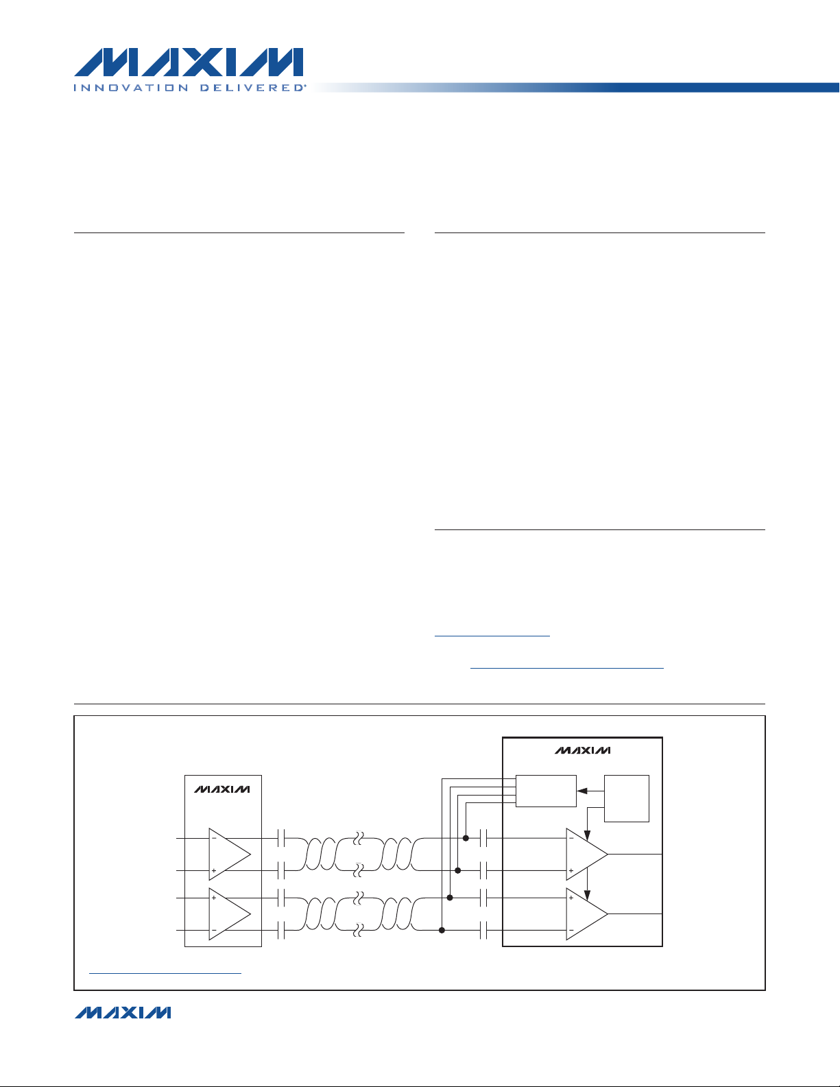
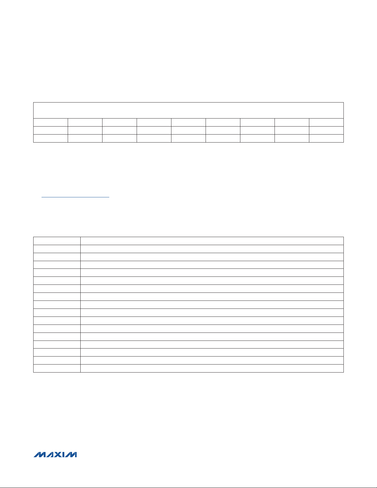
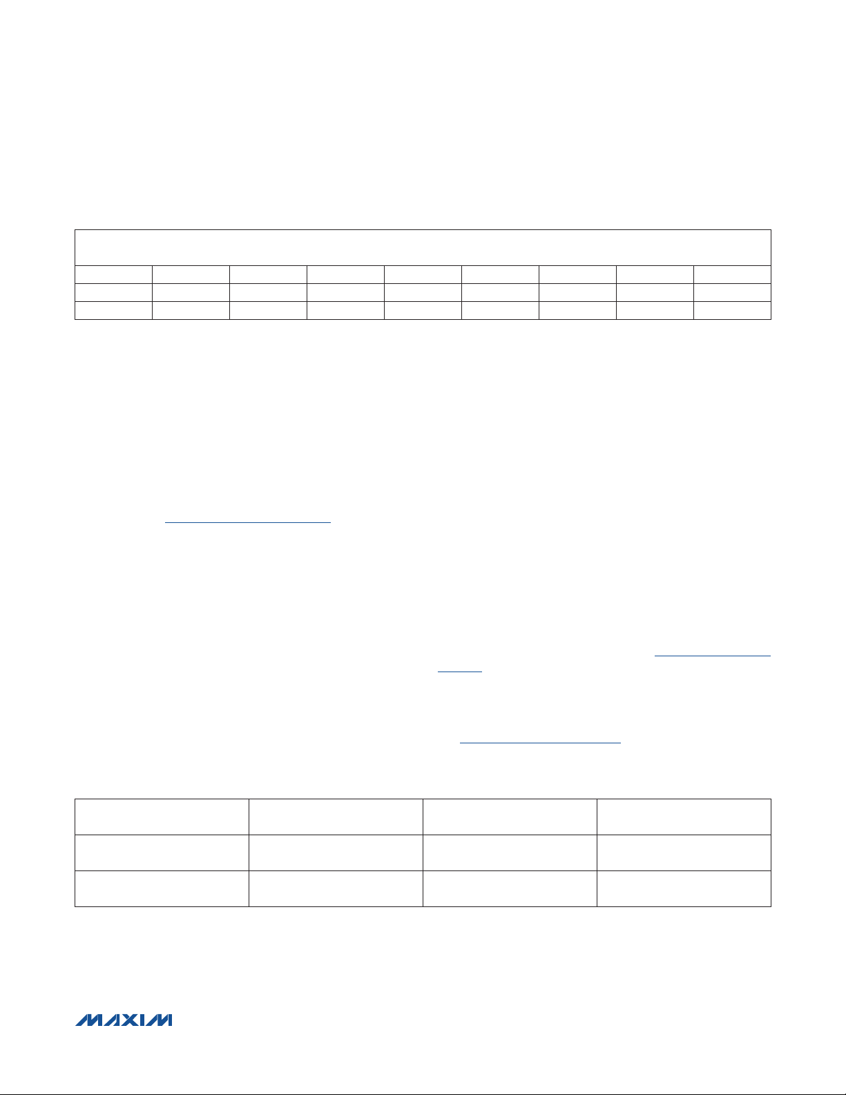
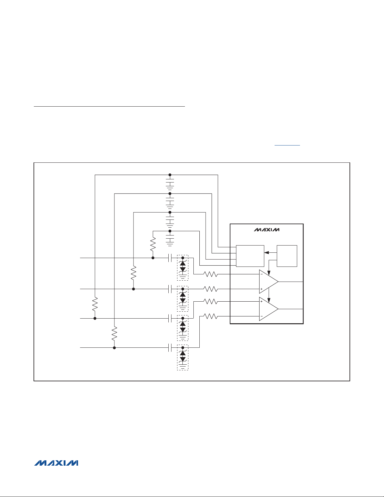
Typical Application Circuits
MAX13335E/MAX13336E
MAX13325
DIAGNOSTICS
MAX13326
PGA
PGA
Typical Application Circuits continued at end of data sheet.
����������������������������������������������������������������� Maxim Integrated Products 1
For pricing, delivery, and ordering information, please contact Maxim Direct at 1-888-629-4642,
or visit Maxim’s website at www.maxim-ic.com.
I2C
AND
CONTROL
Page 2
MAX13335E/MAX13336E
Dual Automotive Differential Audio Receivers
with I2C Control and Diagnostics
ABSOLUTE MAXIMUM RATINGS
VDD to GND ............................................................. -0.3V to +6V
D_ to GND .............................................................. -16V to +28V
INL_, INR_ to GND ................................................. -10V to +15V
OUTR, OUTL to GND ............................... -0.3V to (VDD + 0.3V)
SDA, SCL, INT to GND ............................................ -0.3V to +6V
REF to GND .............................................. -0.3V to (VDD + 0.3V)
Output Short-Circuit Duration ....................................Continuous
Stresses beyond those listed under “Absolute Maximum Ratings” may cause permanent damage to the device. These are stress ratings only, and functional operation of the device at these or any other conditions beyond those indicated in the operational sections of the specifications is not implied. Exposure to absolute
maximum rating conditions for extended periods may affect device reliability.
PACKAGE THERMAL CHARACTERISTICS (Note 1)
QSOP
Junction-to-Ambient Thermal Resistance (BJA) .....103.7NC/W
Junction-to-Case Thermal Resistance (BJC) ...............37NC/W
Note 1: Package thermal resistances were obtained using the method described in JEDEC specification JESD51-7, using a four-
layer board. For detailed information on package thermal considerations, refer to www.maxim-ic.com/thermal-tutorial.
Continuous Power Dissipation (TA = +70NC)
QSOP (derate 9.6 mW/NC above +70°C) ................771.5 mW
Operating Junction Temperature Range ......... -40NC to +150NC
Storage Temperature Range ............................ -65NC to +150NC
Lead Temperature (soldering, 10s) ................................+300NC
Soldering Temperature (reflow) ......................................+260NC
ELECTRICAL CHARACTERISTICS
(VDD = 5V, AV = -6dB, RL = 10kI, f = 20Hz to 20kHz, TA = TJ = -40NC to +105NC, unless otherwise noted. Typical values are at
TA = 25NC under normal conditions, unless otherwise noted.) (Note 2)
PARAMETER SYMBOL CONDITIONS MIN TYP MAX UNITS
GENERAL
V
= 1.68V -5% 3.3 +5%
Supply-Voltage Range V
Quiescent Supply Current I
Shutdown Supply Current I
REF Output Voltage V
Thermal Shutdown T
Thermal Shutdown Hysteresis T
DD
DD
SHDN
REF
SHDN
HYS
REF
V
= 2.5V -5% 5.0 +5%
REF
V
= V
INL_
SHDN bit = 1 6 10
V
= 3.3V -4% 1.68 +4%
DD
V
= 5V -3% 2.5 +3%
DD
(Note 3) +150 °C
(Note 3) 15 °C
= VDD/2 11 mA
INR_
FA
V
V
����������������������������������������������������������������� Maxim Integrated Products 2
Page 3
MAX13335E/MAX13336E
Dual Automotive Differential Audio Receivers
with I2C Control and Diagnostics
ELECTRICAL CHARACTERISTICS (continued)
(VDD = 5V, AV = -6dB, RL = 10kI, f = 20Hz to 20kHz, TA = TJ = -40NC to +105NC, unless otherwise noted. Typical values are at
TA = 25NC under normal conditions, unless otherwise noted.) (Note 2)
PARAMETER SYMBOL CONDITIONS MIN TYP MAX UNITS
AMPLIFIERS
Programmable Gain Amp A
Gain Error A
Gain Matching A
V
ERR
MCH
G_[3:0] = 0000
G_[3:0] = 0001 -12
G_[3:0] = 0010 -10
G_[3:0] = 0011 -8
G_[3:0] = 0100 -6
G_[3:0] = 0101 -4
G_[3:0] = 0110 -2
G_[3:0] =0111 0
G_[3:0] =1000 2
G_[3:0] =1001 4
G_[3:0] =1010 6
G_[3:0] =1011 8
G_[3:0] =1100 10
G_[3:0] =1101 12
G_[3:0] =1110 14
G_[3:0] =1111 16
G_[3:0] = 0000
G_[3:0] = 0001 -20
G_[3:0] = 0010 -18
G_[3:0] = 0011 -16
G_[3:0] = 0100 -14
G_[3:0] = 0101 -12
G_[3:0] = 0110 -10
G_[3:0] =0111 -8
G_[3:0] =1000 -6
G_[3:0] =1001 -4
G_[3:0] =1010 -2
G_[3:0] =1011 0
G_[3:0] =1100 2
G_[3:0] =1101 4
G_[3:0] =1110 6
G_[3:0] =1111 8
Within VCM operating range
Within VCM operating range
MAX13335E
MAX13336E
-14
-22
Q0.4
Q0.4
dB
dB
dB
����������������������������������������������������������������� Maxim Integrated Products 3
Page 4

MAX13335E/MAX13336E
Dual Automotive Differential Audio Receivers
with I2C Control and Diagnostics
ELECTRICAL CHARACTERISTICS (continued)
(VDD = 5V, AV = -6dB, RL = 10kI, f = 20Hz to 20kHz, TA = TJ = -40NC to +105NC, unless otherwise noted. Typical values are at
TA = 25NC under normal conditions, unless otherwise noted.) (Note 2)
PARAMETER SYMBOL CONDITIONS MIN TYP MAX UNITS
Input Offset Voltage V
Input Impedance R
Common-Mode Rejection Ratio A
Power-Supply Rejection Ratio A
Input Voltage Range V
Input Common-Mode Voltage
Range
IOS
CMRR
PSRR
V
CM
AV = 0dB -10 +10 mV
Differential
IN
Single-ended
Within VCM range,
f = DC, AV = -2dB
(Note 4)
VCM = 2V
f = 20Hz to 20kHz
(Note 3)
Within VCM range,
f = DC, AV = -10dB
(Note 4)
VCM = 2V
f = 20Hz to 20kHz
(Note 3)
f = 1kHz, V
Quasi-differential
source, VDD = 3.3V
Quasi-differential
source, VDD = 5V
Differential source,
V
DD
Differential source,
V
IN
DD
Quasi-differential
source, VDD = 3.3V
Quasi-differential
source, VDD = 5V
Differential source,
V
DD
Differential source,
V
DD
V
DD
V
DD
V
DD
V
DD
,
RMS
,
RMS
RIPPLE
= 3.3V
= 5V
= 3.3V
= 5V
= 3.3V
= 5V -1.8 7.0
= 3.3V
= 5V -5.0 11.5
MAX13335E 13.5 22 33
MAX13336E 19 30 42
MAX13335E 8.5 14 21
MAX13336E 11 17 24
60 80
MAX13335E
60
65 85
MAX13336E
65
= 200mV
(Note 3) -80 dB
P-P
MAX13335E
MAX13336E
MAX13335E
MAX13336E
-1.2 4.6
-3.3 7.6
1.3
2
2.6
4.0
2.3
3.5
4.6
7.0
V
kI
dB
RMS
V
����������������������������������������������������������������� Maxim Integrated Products 4
Page 5
MAX13335E/MAX13336E
Dual Automotive Differential Audio Receivers
with I2C Control and Diagnostics
ELECTRICAL CHARACTERISTICS (continued)
(VDD = 5V, AV = -6dB, RL = 10kI, f = 20Hz to 20kHz, TA = TJ = -40NC to +105NC, unless otherwise noted. Typical values are at
TA = 25NC under normal conditions, unless otherwise noted.) (Note 2)
PARAMETER SYMBOL CONDITIONS MIN TYP MAX UNITS
V
-
Output Voltage Range V
Total Harmonic Distortion Plus
Noise
OUT
THD+N f = 1kHz, V
Signal-to-Noise Ratio SNR
Output Noise V
RL = 10kW
V
OUT_
(Note 3)
AV = 0dB, unweighted
N
(Note 3)
= 1.4V
OUT_
RMS
= 1.4V
(Note 3) 0.01 %
RMS
MAX13335E 104.8
MAX13336E 99.4
MAX13335E 8
MAX13336E 15
0.1
Slew Rate SR CL = 300pF (Note 3) 0.5
Maximum Capacitive Load C
Crosstalk A
XTALKVIN
Mute Attenuation A
Shutdown Attenuation A
SHDN
MUTE
No sustained oscillation (Note 3) 300 pF
L
= 2V
MUTE bit = 1, V
SHDN bit = 1, V
(Note 3) -80 dB
RMS
IN
IN
= 2V
= 2V
(Note 3) -80 dB
RMS
(Note 3) -80 dB
RMS
LEVEL SENSE/CLIP DETECTION
Audio Presence Threshold V
Clip-Level Warning
V
V
TAP
TCP
TCN
Output referred 127 200 268 mV
Positive clip warning level 90
Negative clip warning level 10
DIAGNOSTIC I/O
D_[3:0]=0001 40
D_[3:0]=0010 97
D_[3:0]=0011 154
D_[3:0]=0100 210
D_[3:0]=0101 265
D_[3:0]=0110 320
Pullup Current Limit I
IDH
V
D_
= 1.5V
D_[3:0]=0111 375
D_[3:0]=1000 430
D_[3:0]=1001 485
D_[3:0]=1010 540
D_[3:0]=1011 595
D_[3:0]=1100 650
D_[3:0]=1101 705
Pulldown Current I
Trip High Threshold V
Trip Low Threshold V
Switch Diode V
Input Resistance R
IDL
IDH
IDL
DON
DOFF
D_[3:0] = 1110, V
R
= 1kI to 10kI
D_
R
= 1kI to 10kI
D_
D_
< V
CM
D_[3:0] = 1111 0.7 V
Off-state D_[3:0] = 0000, V
D_
< V
CM
32 65
1.94 V
0.92 V
1
DD
0.1
FV
V/Fs
% V
MI
V
dB
RMS
RMS
DD
FA
FA
����������������������������������������������������������������� Maxim Integrated Products 5
Page 6

MAX13335E/MAX13336E
Dual Automotive Differential Audio Receivers
with I2C Control and Diagnostics
ELECTRICAL CHARACTERISTICS (continued)
(VDD = 5V, AV = -6dB, RL = 10kI, f = 20Hz to 20kHz, TA = TJ = -40NC to +105NC, unless otherwise noted. Typical values are at
TA = 25NC under normal conditions, unless otherwise noted.) (Note 2)
PARAMETER SYMBOL CONDITIONS MIN TYP MAX UNITS
Leakage Current I
DLKG
ESD PROTECTION
ISO 10605 Air Gap V
Contact Discharge V
ESD
ESD
DIGITAL INTERFACE
Input Voltage High V
Input Voltage Low V
Input Voltage Hysteresis V
I/O Leakage Current I
Output Low Voltage V
EN to Full Operation Time t
INH
INL
HYS
LKG
OL
SON
I2C TIMING
Output Fall Time t
OF
Pin Capacitance C
Clock Frequency f
SCL Low Time t
SCL High Time t
START Condition Hold Time t
START Condition Setup Time t
Data Hold Time t
Data Setup Time t
SCL
LOW
HIGH
HD:STA
SU:STA
HD:DAT
SU:DAT
Input Rise Time t
Input Fall Time t
STOP Condition Setup Time t
Bus Free Time t
Maximum Bus Capacitance C
SU:STO
BUF
BUS
Note 2: Specifications within minimum and maximum limits are 100% production tested at TA = +25NC and are guaranteed over
the operating temperature range by design and characterization. Actual typical values may vary and are not guaranteed.
Note 3: Guaranteed by bench characterization.
Note 4: A
CMRR
= 20log(δV
IOS
/δVCM).
Off-state D_[3:0] = 0000, V
D_
< V
CM
Q10 FA
2kI/150pF, INL_, INR_ Q15
330I/330pF, INL_, INR_ Q8
SDA, SCL
0.7 x
V
DD
SDA, SCL
0.14 x
V
DD
Q10 FA
100 ms
IN
SDA, SCL
SDA, SCL, INT
SDA, INT, I
C
= 2.2FF (Note 3)
REF
C
= 10pF to 400pF 250 ns
BUS
SINK
= 3mA
1.3
0.6
Repeated START condition 0.6
Repeated START condition 0.6
0 900 ns
100 ns
SCL, SDA 300 ns
R
SCL, SDA 300 ns
F
0.6
Between START and STOP conditions 1.3
Per bus line 400 pF
kV
kV
0.3 x
V
DD
mV
0.4 V
10 pF
400 kHz
V
V
Fs
Fs
Fs
Fs
Fs
Fs
����������������������������������������������������������������� Maxim Integrated Products 6
Page 7
MAX13335E/MAX13336E
Dual Automotive Differential Audio Receivers
with I2C Control and Diagnostics
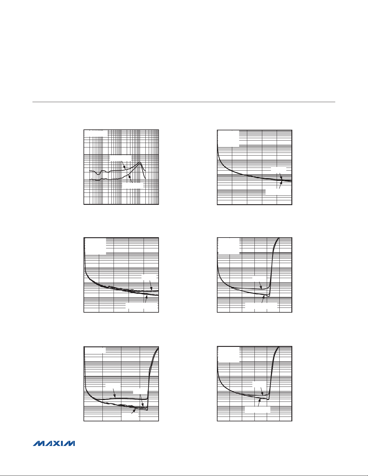
Typical Operating Characteristics
(VDD = 5V, AV = -6dB, R
0.1
0.01
THD+N (%)
0.001
0.0001
0.01 100
10
1
0.1
THD+N (%)
0.01
= 10kI, BW = 20Hz to 20kHz, T
L
THD+N vs. FREQUENCY
V
= 2V
IN_
RMS
MAX13336E
MAX13335E
1010.1
FREQUENCY (kHz)
THD+N vs. OUTPUT VOLTAGE
MAX13335E
= 5V
V
DD
= -18dB
A
V
f = 6kHz
= +25NC, unless otherwise noted.)
A
THD+N vs. OUTPUT VOLTAGE
10
MAX13336E
= 5V
V
DD
= -22dB
A
V
MAX13335E toc01
1
0.1
THD+N (%)
0.01
0.001
0.0001
0 0.5
THD+N vs. OUTPUT VOLTAGE
10
MAX13336E
= 5V
V
DD
AV = -6dB
MAX13335E toc03
1
0.1
THD+N (%)
0.01
OUTPUT VOLTAGE (V
f = 6kHz
f = 6kHz
f = 100Hz, 1kHz
0.40.30.20.1
)
RMS
MAX13335E toc02
MAX13335E toc04
0.001
f = 100Hz AND 1kHz
0.0001
0 0.5
OUTPUT VOLTAGE (V
THD+N vs. OUTPUT VOLTAGE
10
MAX13335E
1
0.1
THD+N (%)
0.01
0.001
0.0001
0 2.0
f = 6kHz
f = 100Hz
OUTPUT VOLTAGE (V
RMS
f = 1kHz
1.51.00.5
RMS
0.40.30.20.1
)
MAX13335E toc05
)
0.001
f = 100Hz AND 1kHz
0.0001
0 2.4
OUTPUT VOLTAGE (V
THD+N vs. OUTPUT VOLTAGE
10
MAX13336E
= 5V
V
DD
= 8dB
A
V
1
0.1
THD+N (%)
0.01
0.001
0.0001
0 2.4
OUTPUT VOLTAGE (V
f = 6kHz
f = 100Hz, 1kHz
RMS
RMS
2.01.61.20.80.4
)
MAX13335E toc06
2.01.61.20.80.4
)
����������������������������������������������������������������� Maxim Integrated Products 7
Page 8
MAX13335E/MAX13336E
Dual Automotive Differential Audio Receivers
with I2C Control and Diagnostics
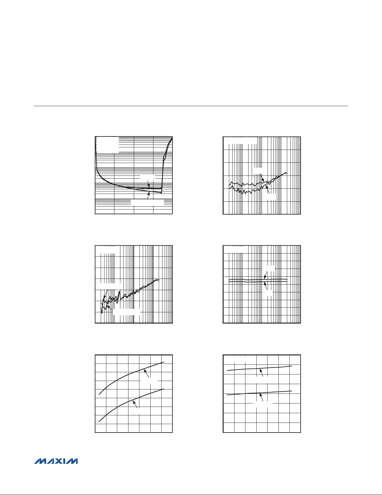
Typical Operating Characteristics (continued)
(VDD = 5V, AV = -6dB, R
0.1
THD+N (%)
0.01
0.001
0.0001
-80
-90
-100
-110
-120
CMRR (dB)
-130
-140
-150
= 10kI, BW = 20Hz to 20kHz, T
L
THD+N vs. OUTPUT VOLTAGE
10
MAX13335E
= 5V
V
DD
= +12dB
A
V
1
f = 6kHz
f = 100Hz AND 1kHz
RMS
1.51.00.5
)
0 2.0
OUTPUT VOLTAGE (V
CROSSTALK vs. FREQUENCY
V
= 2V
IN_
RMS
OUTR TO OUTL
OUTL TO OUTR
0.01 100
FREQUENCY (kHz)
1010.1
= +25NC, unless otherwise noted.)
A
POWER-SUPPLY REJECTION RATIO
vs. FREQUENCY
-60
V
= 200mV
RIPPLE
MAX13335E toc07
-70
-80
-90
PSRR (dB)
-100
-110
-120
0.01 100
GAIN MATCHING vs. FREQUENCY
-5.80
V
= 2V
IN_
-5.85
MAX13335E toc09
-5.90
-5.95
-6.00
-6.05
GAIN (dB)
-6.10
-6.15
-6.20
-6.25
-6.30
0.01 100
RMS
P-P
MAX13335E toc08
OUTR
OUTL
1010.1
FREQUENCY (kHz)
MAX13335E toc10
OUTR
OUTL
1010.1
FREQUENCY (kHz)
SUPPLY CURRENT vs. TEMPERATURE
12.0
11.8
11.6
11.4
11.2
11.0
10.80
SUPPLY CURRENT (mA)
10.60
10.40
10.20
-50 125
TEMPERATURE (°C)
VDD = 5V
VDD = 3.3V
MAX13335E toc11
1007525 500-25
SHUTDOWN CURRENT vs. TEMPERATURE
8
VDD = V
= V
SCL
7
6
5
4
3
SHUTDOWN CURRENT (µA)
2
1
0
-50 125
SDA
VDD = 5V
VDD = 3.3V
TEMPERATURE (°C)
MAX13335E toc12
10075-25 0 25 50
����������������������������������������������������������������� Maxim Integrated Products 8
Page 9
MAX13335E/MAX13336E
01
01
01
Dual Automotive Differential Audio Receivers
with I2C Control and Diagnostics
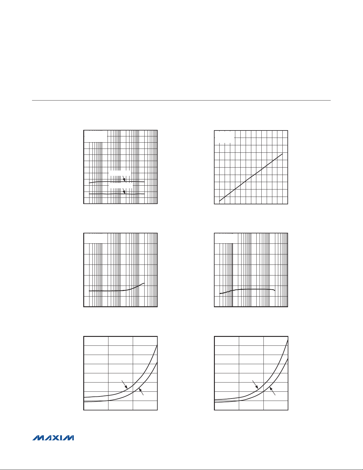
Typical Operating Characteristics (continued)
(VDD = 5V, AV = -6dB, R
0
-10
-20
-30
-40
-50
-60
CMRR (dB)
-70
-80
-90
-100
-110
-120
0.01 100
0
-20
-40
-60
-80
= 10kI, BW = 20Hz to 20kHz, T
L
COMMON-MODE REJECTION RATIO
vs. FREQUENCY
MAX13336E
= 2V
V
IN_
RMS
LEFT CHANNEL
RIGHT CHANNEL
1010.1
FREQUENCY (kHz)
MUTE ATTENUATION vs. FREQUENCY
V
= 2V
IN_
RMS
MUTE = 1
= +25NC, unless otherwise noted.)
A
DIAGNOSTIC CURRENT SOURCE vs. D_[3:0]
1000
VDD = 5V
900
= 1.5V
V
D_
(µA)
D_
I
800
700
600
500
400
300
200
100
0
MAX13335E toc13
SHUTDOWN ATTENUATION vs. FREQUENCY
0
V
= 2V
IN_
SHDN = 1
MAX13335E toc15
-20
-40
-60
-80
RMS
D_[3:0] (dec)
MAX13335E toc14
131210 113 4 5 6 7 8 91 2
4
MAX13335E toc16
-100
MUTE ATTENUATION (dB)
-120
-140
0.01 100
FREQUENCY (kHz)
1010.1
OUTPUT NOISE vs. GAIN SETTING
40
MAX13336E
35
)
30
RMS
25
20
15
OUTPUT NOISE (µV
10
5
0
NONWEIGHTED
G_[3:0] (dec)
A-WEIGHTED
105
5
����������������������������������������������������������������� Maxim Integrated Products 9
MAX13335E toc17
-100
SHUTDOWN ATTENUATION (dB)
-120
-140
0.01 100
FREQUENCY (kHz)
OUTPUT NOISE vs. GAIN SETTING
40
MAX13335E
35
)
30
RMS
25
20
15
OUTPUT NOISE (µV
10
5
0
NONWEIGHTED
A-WEIGHTED
105
G_[3:0] (dec)
1010.1
MAX13335E toc18
5
Page 10

MAX13335E/MAX13336E
Dual Automotive Differential Audio Receivers
with I2C Control and Diagnostics
Pin Configuration
TOP VIEW
1
2
3
4
5
6
7
8
+
MAX13335E
MAX13336E
16
REF
15
V
DD
OUTL
14
GND
13
OUTR
12
INT
11
SDA
10
SCL
9
D0
D1
INL+
INL-
INR-
INR+
D2
D3
QSOP
PIN NAME FUNCTION
1 D0 Diagnostic I/O 0. I/O pin used for jack sense and diagnostics.
2 D1 Diagnostic I/O 1. I/O pin used for jack sense and diagnostics.
3 INL+ Noninverting Left-Channel Audio Input
4 INL- Inverting Left-Channel Audio Input
5 INR- Inverting Right-Channel Audio Input
6 INR+ Noninverting Right-Channel Audio Input
7 D2 Diagnostic I/O 2. I/O pin used for diagnostics.
8 D3 Diagnostic I/O 3. I/O pin used for diagnostics.
9 SCL I2C Serial-Clock Input
10 SDA I2C Serial-Data Input and Output
11
INT
Active-Low, Open-Drain Interrupt Request Output
12 OUTR Right-Channel Audio Output
13 GND Ground
14 OUTL Left-Channel Audio Output
15 V
DD
16 REF
Supply Input
VDD/2 Reference Output. Bypass REF to GND with a 2.2FF capacitor.
Pin Description
���������������������������������������������������������������� Maxim Integrated Products 10
Page 11

MAX13335E/MAX13336E
Dual Automotive Differential Audio Receivers
with I2C Control and Diagnostics
Detailed Description
The MAX13335E/MAX13336E are designed to operate
with the MAX13325/MAX13326 dual automotive audio
line drivers to form a complete differential audio link
in automotive systems. In addition, the MAX13335E/
MAX13336E can operate as an auxiliary input audio
amplifier with jack sense function.
Signal Path
The devices can be configured to operate with quasi-differential (up to 3.5V
input signals. Both input channels feature high 80dB CMRR
(typ). An integrated programmable gain amplifier with zerocrossing detection controlled through the I2C interface provides adjustable gain from -14dB to +16dB (MAX13335E)
or -22dB to +8dB (MAX13336E) in +2dB increments. Zerocrossing detection can be enabled to limit the zip noise
during a gain transition by delaying the gain change until a
zero-crossing event occurs on the input signal.
The devices can monitor the inputs for the presence of
audio, clip detection, and change-of-state in the jack sense.
An active-low, open-drain interrupt request output can be
configured through the I2C interface to report the presence
of audio, clip detection, and change-of-state in the jack
sense. The internal status register also latches the status
change of those parameters until an I2C read is performed.
D_
R
D_
Figure 1. Diagnostic I/O Port
) and fully differential (up to 7V
RMS
Interrupt Output
40µA TO
705µA
V
IDH
V
IDL
DH_
DL_
I2C INTERFACE
RMS
)
Thermal Shutdown
Thermal shutdown protects the device when the junction
temperature exceeds +150NC (typ). The device resumes
operation when the junction temperature drops below the
thermal shutdown hysteresis of 15NC (typ). The internal
status register latches the status change of the TSD bit
until an I2C read is performed.
Diagnostics
The devices feature four similar diagnostic I/O ports.
When configured correctly, they are capable of performing jack sense detection, short-to-ground, short-tobattery, open-load, and shorts between channels. Each
diagnostic I/O port contains a programmable current
source, a voltage sense, and a diode to ground.
The principle behind the diagnosis is simply forcing a
current into the load attached to the I/O port and sensing
the voltage to check if it is greater or smaller than the
two predefined low/high thresholds. These can be easily
accessed by a microcontroller through the I2C interface.
The procedure usually starts with stepping up the current
source from the minimum to maximum range.
1) If the sensed voltage is consistently below the low
threshold, a short-to-ground event is determined.
2) However, if the sensed voltage is consistently above
the high threshold, there is a possibility of either a
short-to-battery or an open-load event. In order to differentiate between them, the I/O port should be tested
again with a voltage-sense-only configuration (i.e.,
with the current source switched off). If the sensed
voltage remains above the high threshold, a short-tobattery event has occurred. Otherwise, an open-load
event is detected.
3) In some current source range, if the sensed voltage
is between the high and low thresholds, this could
indicate that the load is present.
A valid readout of the status might require some amount
of delays (to be inserted by the microcontroller) due to
the settling time needed to charge/discharge any external capacitive load on the I/O port.
The diode is useful in the case of sensing an unconnected load or short between channels. Here, one end
of the load can be forced to ground by the diode and
the usual procedure described above can be applied to
detect various events. It is, however, advisable to test the
I/O port for a short-to-battery condition prior to turning on
the diode as it could risk damaging the device.
���������������������������������������������������������������� Maxim Integrated Products 11
Page 12

MAX13335E/MAX13336E
Dual Automotive Differential Audio Receivers
with I2C Control and Diagnostics
See the Applications Information section for various
examples on how the diagnostic can be set up to detect
different events.
Applications Information
Serial Interface
Writing to the device using I2C requires that first the master send a START condition (S) followed by the device’s
I2C address. After the address, the master sends the
address of the register that is to be programmed. The
master then ends communication by issuing a STOP condition (P) to relinquish control of the bus, or a repeated
START condition (Sr) to communicate to another I2C
slave (Figure 2).
Bit Transfer
Each SCL rising edge transfers one data bit. The data
on SDA must remain stable during the high portion of the
SCL clock pulse (Figure 3). Changes in SDA while SCL
SDA
t
t
F
t
LOW
SU:DAT
t
R
t
F
is high are read as control signals (see the START and
STOP Conditions section). When the serial interface is
inactive, SDA and SCL idle high.
START and STOP Conditions
A master device initiates communication by issuing a
START condition (S) which is a high-to-low transition on
SDA with SCL high. A START condition from the master
signals the beginning of a transmission to the device.
The master terminates transmission by a STOP condition (P) (see the Acknowledge Bit section). A STOP
condition is a low-to-high transition on SDA while SCL is
high (Figure 4). The STOP condition frees the bus. If a
repeated START condition (Sr) is generated instead of a
STOP condition, the bus remains active. When a STOP
condition or incorrect slave ID is detected, the device
internally disconnects SCL from the serial interface until
the next START or repeated START condition, minimizing digital noise and feedthrough.
t
t
HD:STA
t
SP
R
t
BUF
SCL
t
HD:STA
t
HD:DAT
t
HIGH
t
SU:STA
t
SU:STO
Figure 2. I2C Timing
START
SDA
SCL
DATA LINE
STABLE;
DATA VALID
CHANGE OF
DATA ALLOWED
CONDITION
SDA
SCL
Figure 3. Bit Transfer Figure 4. START/STOP Conditions
���������������������������������������������������������������� Maxim Integrated Products 12
SPSrS
STOP
CONDITION
Page 13

MAX13335E/MAX13336E
Dual Automotive Differential Audio Receivers
with I2C Control and Diagnostics
Acknowledge Bit
The acknowledge bit (ACK) is a clocked 9th bit that the
device uses to handshake the receipt of each byte of
data when in write mode. The device pulls down SDA
during the entire master-generated 9th clock pulse if
the previous byte is successfully received (Figure 5).
Monitoring ACK allows for detection of unsuccessful
data transfers. An unsuccessful data transfer occurs
if a receiving device is busy or if a system fault has
occurred. In the event of an unsuccessful data transfer,
the bus master could retry communication. The master must pull down SDA during the 9th clock cycle to
acknowledge receipt of data when the device is in read
mode. An acknowledge must be sent by the master
after each read byte to allow data transfer to continue.
S
SDA
SCL
18
A not-acknowledge is sent when the master reads the
final byte of data from the device, followed by a STOP
condition.
Slave Address
The device is programmable to one of the four I2C slave
addresses (Table 2). The power-on default I2C slave address
of the device for read/write is 0xD0/0xD1 (1101000R/W). The
I2C slave address of the device can be selected by writing
to Control Register 1 (0x03) while INT is pulled low externally
during the I2C write duration (Figure 6).
Single Byte-Write Operation
For a single byte-write operation, send the slave address
as the first byte followed by the register address and then
a single data byte (Figure 7).
NOT ACKNOWLEDGE
ACKNOWLEDGE
9
Figure 5. Acknowledge and Not-Acknowledge Bits
CONTROL REGISTER 1 (0x03) PROGRAM I
SDA 11 11100 00000
SCL
INT
Figure 6. I2C Slave Address Programming
S S7 S6 S5 S4 S3 S2 S1 ACK
SLAVE ADDRESS
B7 B6 B5 B4 B3 B2 B1 B0 ACK P
DATA 1
Figure 7. A Single Byte-Write Operation
���������������������������������������������������������������� Maxim Integrated Products 13
R/W
= 0
2
C ADDRESSCURRENT I2C ADDRESS
00000000 ACK ACK ACKI2C1 I2C1I2C0 I2C0
C7 C6 C5 C4 C3 C2 C1 C0 ACK
REGISTER ADDRESS
Page 14

MAX13335E/MAX13336E
Dual Automotive Differential Audio Receivers
with I2C Control and Diagnostics
Burst-Write Operation
For a burst-write operation, send the slave address as
the first byte followed by the register address and then
the data bytes (Figure 8).
Single Byte-Read Operation
For a single byte-read operation, send the slave address
with read bit set as the first byte followed by the register
address. Then send a repeated START condition followed by the slave address. After the slave sends the
S S7 S6 S5 S4 S3 S2 S1 ACK
SLAVE ADDRESS
B7 B6 B5 B4 B3 B2 B1 B0 ACK B7 B6 B5 B4 B3 B2 B1 B0 ACK
DATA 1
Figure 8. A Burst-Write Operation
R/W
= 0
ACK B7 B6 B5 B4 B3 B2 B1 B0 ACK P
data byte, send a not-acknowledge followed by a STOP
condition (Figure 9).
Burst-Read Operation
For a burst-read operation, send the slave address with
a write as the first byte followed by the register address.
Then send a repeated START condition followed by the
slave address. The slave sends data bytes until a notacknowledge condition is sent (Figure 10).
R7 R6 R5 R4 R3 R2 R1 R0 ACK
REGISTER ADDRESS
DATA 2
DATA N
S S7 S6 S5 S4 S3 S2 S1 ACK B7 B6 B5 B4 B3 B2 B1 B0 ACK
SLAVE ADDRESS REGISTER ADDRESS
Sr
S7 S6 S5 S4 S3 S2 S1 ACK B7 B6 B5 B4 B3 B2 B1 B0 NACK P
SLAVE ADDRESS DATA
NOTE: SHADED ITEM IS FROM THE MASTER.
Figure 9. A Single Byte-Read Operation
S S7 S6 S5 S4 S3 S2 S1 ACK B7 B6 B5 B4 B3 B2 B1 B0 ACK
SLAVE ADDRESS REGISTER ADDRESS
Sr S7 S6 S5 S4 S3 S2 S1 ACK B7 B6 B5 B4 B3 B2 B1 B0 ACK
SLAVE ADDRESS DATA 1
NOTE: SHADED ITEMS ARE FROM THE MASTER.
Figure 10. A Burst-Read Operation
���������������������������������������������������������������� Maxim Integrated Products 14
R/W
= 0
R/W
= 1
R/W
= 0
R/W
= 1
ACK B7 B6 B5 B4 B3 B2 B1 B0 NACK P
DATA N
Page 15

MAX13335E/MAX13336E
Dual Automotive Differential Audio Receivers
with I2C Control and Diagnostics
Register Map
NAME REG BIT 7 BIT 6 BIT 5 BIT 4 BIT 3 BIT 2 BIT 1 BIT 0 R/W POR SETTINGS
STAT0 00 DH3 DL3 DH2 DL2 DH1 DL1 DH0 DL0 R 0x00
STAT1 01 APD CLD JSD TSD — ID2 ID1 ID0 R 0x00
CTRL0 02 API CLI JSI — — ZEN MUTE SHDN
CTRL1 03 — — — — — — I2C1 I2C0
DIAG0 04 D1[3] D1[2] D1[1] D1[0] D0[3] D0[2] D0[1] D0[0]
DIAG1 05 D3[3] D3[2] D3[1] D3[0] D2[3] D2[2] D2[1] D2[0]
GAIN 06 GL3 GL2 GL1 GL0 GR3 GR2 GR1 GR0
R/W
R/W
R/W
R/W
R/W
Status Register 0 (STAT0)
ADDRESS: 0x00
MODE: R
BIT 7 6 5 4 3 2 1 0
NAME
POR
DH3 DL3 DH2 DL2 DH1 DL1 DH0 DL0
0 0 0 0 0 0 0 0
0x00
0x00
0x00
0x00
0x00
The bits in Status Register 0 are updated to reflect the states of the upper (DH_) and lower (DL_) comparator’s threshold
when voltage sensing is enabled for the corresponding diagnostic I/O. Combinations of DH_ and DL_ can be used to
decode the fault on the I/O port.
Bits 7, 5, 3, 1: DH� (Diagnostic Upper Comparator Threshold V
IDH
)
0 = Below upper threshold
1 = Above upper threshold
Bits 6, 4, 2, 0: DL� (Diagnostic Lower Comparator Threshold V
IDL
)
0 = Below lower threshold
1 = Above lower threshold
Table 1. Interpretation of Diagnostic Status Bits
DH� DL� CONDITION
0 0 Short-to-ground (or disabled)
0 1 No fault
1 0 Invalid (not used)
1 1 Short-to-battery if current source is disabled (i.e., D_[3:0] = 1110)
1 1 Open-load if current source is enabled (i.e., D_[3:0] = 0001 to 1101)
���������������������������������������������������������������� Maxim Integrated Products 15
Page 16

MAX13335E/MAX13336E
Dual Automotive Differential Audio Receivers
with I2C Control and Diagnostics
Status Register 1 (STAT1)
ADDRESS: 0x01
MODE: R
BIT 7 6 5 4 3 2 1 0
NAME
POR
Bit 7: APD (Audio Presence Status Bit)
0 = Audio not present.
1 = Audio presence detected. INT asserts low.
Bit 6: CLD (Clip Detection Status Bit)
0 = No clipping detected.
1 = Clip warning. INT asserts low.
Bit 5: JSD (Jack Sense Status Bit)
0 = Jack removed. INT asserts low.
1 = Jack inserted. INT asserts low.
Note: INT asserts low whenever jack sense changes state.
Bit 4: TSD (Thermal Shutdown Status Bit)
0 = Within safe operating range.
1 = Overheating detected. INT pin asserts low.
Bit 3: No Function
Bit 2 to 0: ID� (Die ID)
001 = MAX13335E
010 = MAX13336E
Note: Reading of Status Register 1 (REG = 0x01) releases INT and resets bits APD, CLD, JSD, and TSD back to zero.
APD CLD JSD TSD — ID2 ID1 ID0
0 0 0 0 0 — — —
���������������������������������������������������������������� Maxim Integrated Products 16
Page 17
MAX13335E/MAX13336E
Dual Automotive Differential Audio Receivers
with I2C Control and Diagnostics
Control Register 0 (CTRL0)
ADDRESS: 0x02
MODE: R/W
BIT 7 6 5 4 3 2 1 0
NAME
POR
Bit 7: API (Audio Presence Interrupt Enable Bit)
0 = Disable
1 = Enable*
*Bit automatically resets to 0 when an audio presence interrupt occurs.
Bit 6: CLI (Clip Warning Interrupt Enable Bit)
0 = Disable
1 = Enable*
*Bit automatically resets to 0 when a clip warning interrupt occurs.
Bit 5: JSI (Jack Sense Interrupt Enable Bit)
The JSI bit can be set only after D1[3:0] and D0[3:0] in Diagnostic register 0 (DIAG0) has been programmed.
0 = Disable
1 = Enable*
*Bit automatically resets to 0 when a jack sense interrupt occurs.
Bits 4 and 3: No Function (0 should be written during write access.)
Bit 2: ZEN (Zero-Crossing Enable Bit)
Enabling zero-crossing detection loads the new PGA gain settings at the signal zero crossing to avoid zip noise.
0 = Disable
1 = Enable
Bit 1: MUTE (Mute Enable Bite)
0 = Play mode
1 = Mute mode
Bit 0 : SHDN (Shutdown Enable Bit)
0 = Normal mode
1 = Shutdown mode
API CLI JSI — — ZEN MUTE SHDN
0 0 0 0 0 0 0 0
���������������������������������������������������������������� Maxim Integrated Products 17
Page 18

MAX13335E/MAX13336E
Dual Automotive Differential Audio Receivers
with I2C Control and Diagnostics
Control Register 1 (CTRL1)
ADDRESS: 0x03
MODE: R/W
BIT 7 6 5 4 3 2 1 0
NAME
POR
Bits 7 to 2: No Function (0 should be written during write access.)
Bits 1 and 0: I2C�
The I2C1 and I2C0 bits determine the I2C slave address of the device. The I2C slave address is changed by writing to
CTRL1 while INT is pulled low (e.g., by an external microcontroller) for the duration of the I2C write cycle.
Table 2. I2C Address
— — — — — — I2C1 I2C0
0 0 0 0 0 0 0 0
A7 A6 A5 A4 A3 A2 (I2C1) A1 (I2C0)
1 1 0 1 0 0 0 — 0xD1 0xD0
1 1 0 1 0 0 1 — 0xD3 0xD2
1 1 0 1 0 1 0 — 0xD5 0xD4
1 1 0 1 0 1 1 — 0xD7 0xD6
A0 (R/W)
READ WRITE
Diagnostic Register 0 (DIAG0)
ADDRESS: 0x04
MODE: R/W
BIT 7 6 5 4 3 2 1 0
NAME
POR
D1[3] D1[2] D1[1] D1[0] D0[3] D0[2] D0[1] D0[0]
0 0 0 0 0 0 0 0
���������������������������������������������������������������� Maxim Integrated Products 18
Page 19
MAX13335E/MAX13336E
Dual Automotive Differential Audio Receivers
with I2C Control and Diagnostics
Diagnostic Register 1 (DIAG1)
ADDRESS: 0x05
MODE: R/W
BIT 7 6 5 4 3 2 1 0
NAME
POR
The Diagnostic registers, DIAG0 and DIAG1, program the state of the four diagnostic I/O ports D_. The diagnostic ports
can be programmed to operate in one of the four states:
1) Setting D_[3:0] = 0000 disables the corresponding diagnostic I/O.
2) Setting D_[3:0] = 0001 to 1101 enables the internal current source (40FA to 705FA) and voltage sensing. The voltage sensing utilizes a window comparator with an upper threshold of 1.94V and a lower threshold of 0.92V (see the
Diagnostic Configurations section).
3) Setting D_[3:0] = 1110 enables voltage sensing only.
4) Setting D_[3:0] = 1111 enables the internal diode to ground.
Table 3. Diagnostic I/O Port States
D3[3] D3[2] D3[1] D3[0] D2[3] D2[2] D2[1] D2[0]
0 0 0 0 0 0 0 0
D�[3:0] FUNCTION
0000
0001
0010
0011
0100
0101
0110
0111
1000
1001
1010
1011
1100
1101
1110
1111
Diagnostic output disabled.
Enables the 40FA current source and voltage sense.
Enables the 97FA current source and voltage sense.
Enables the 154FA current source and voltage sense.
Enables the 210FA current source and voltage sense.
Enables the 265FA current source and voltage sense.
Enables the 320FA current source and voltage sense.
Enables the 375FA current source and voltage sense.
Enables the 430FA current source and voltage sense.
Enables the 485FA current source and voltage sense.
Enables the 540FA current source and voltage sense.
Enables the 595FA current source and voltage sense.
Enables the 650FA current source and voltage sense.
Enables the 705FA current source and voltage sense.
Enable voltage sense. The current source is disabled.
Enables the diode. The current source and voltage sense are disabled.
���������������������������������������������������������������� Maxim Integrated Products 19
Page 20
MAX13335E/MAX13336E
Dual Automotive Differential Audio Receivers
with I2C Control and Diagnostics
Gain Register (GAIN)
ADDRESS: 0x06
MODE: R/W
BIT 7 6 5 4 3 2 1 0
NAME
POR
Bits 7 to 0: G�
The Gain register sets the gain of the internal programmable gain amplifier (AV) for the left (GL[3:0]) and right (GR[3:0])
channels. The gain of the programmable gain amplifier (AV) is determined by the following transfer function:
GL3 GL2 GL1 GL0 GR3 GR2 GR1 GR0
0 0 0 0 0 0 0 0
Gain(AV) = -14dB + (G_[3:0] x 2)dB (for MAX13335E)
Gain(AV) = -22dB + (G_[3:0] x 2)dB (for MAX13336E)
Diagnostic Configurations
The device’s diagnostics can be configured for local jack
sense, remote jack sense, and differential drive connections (see the Typical Application Circuits). Diagnostic
registers DIAG0 and DIAG1 configure the diagnostic I/O
ports D_ as a current-source output with voltage sensing
enabled, a voltage sensing input, or a diode to GND.
When voltage sensing is enabled, the current states of
the internal window comparator are updated to status
register STAT0. A valid readout of the STAT0 register
might require some amount of delays (to be inserted by
the microcontroller) between configuring the diagnostic
and reading the status register due to the settling time
needed to charge/discharge the external capacitive load
on the D_ pins.
Local Jack Sense
The device is configured for jack sense function when the
jack is localized to the same module. In this application
example, the diagnostic I/O D1 is configured as a 97FA
current-source output and D0 is configured for voltage
sensing. When a plug is not inserted, the internal spring
contact of the jack shorts D1 to D0. The 97FA current
source from D1 pulls D0 to VDD resulting in DH0 = 1.
When a plug is inserted, the internal spring contact of
the jack is forced open and disconnects D1 from D0. This
results in D0 going low and hence DH0 = 0.
Remote Jack Sense Detection
When the jack is remotely located, the device can be
used for additional fault detection of the wiring harness
used for the connection. See the Typical Application
Circuits.
For fully differential applications, the device can be configured to detect faults in the wiring harness as shown in
the Typical Application Circuits.
Table 4. Local Jack Sense Diagnostic Configuration
CONFIGURATION FUNCTION COMPARATOR OUTPUT STATUS
D1[3:0] = 0010
D0[3:0] = 1110
D1[3:0] = 0010
D0[3:0] = 1110
Source 97FA
Source off
Source 97FA
Source off
DH0 = H Device not plugged in
DH0 = L Device plugged in
Differential Connection
���������������������������������������������������������������� Maxim Integrated Products 20
Page 21
MAX13335E/MAX13336E
Dual Automotive Differential Audio Receivers
with I2C Control and Diagnostics
MAX13335E/MAX13336E
D1[3:0] ≥ 0010
97µA
D1
V
IDH
L
V
IDL
R
C
D0[3:0] = 1110
40µA TO
D0
705µA
Figure 11. Diagnostic Setup for Local Jack Sense
Audio Presence Detection
When the device is used in an auxiliary input amplifier, it can detect if audio is present at the inputs so the
downstream DSP does not have to continuously convert
the analog signal to digital in order to monitor the audio
stream. This can save two ADC inputs as the auxiliary
input can be muxed with another audio stream that is
mutually exclusive. To do this, perform the following steps:
V
IDH
DH0
DL0
V
IDL
1) Set the gain in the GAIN register based on the
required input audio level where the APD threshold is
exceeded. The threshold is set to 200mV
RMS
/G_[3:0].
2) Set API bit in the CTRL0 register to enable the APD
interrupt.
When the input audio level exceeds 200mV
RMS
/G_[3:0]
the INT pin is asserted. The microcontroller can read
back the STAT0 register to check for APD = 1.
���������������������������������������������������������������� Maxim Integrated Products 21
Page 22
MAX13335E/MAX13336E
Dual Automotive Differential Audio Receivers
with I2C Control and Diagnostics
MAX13335E/MAX13336E
D1[3:0] = 0000
40µA TO
705µA
40µA TO
705µA
D3[3:0] = 1101
705µA
1kΩ-10kΩ
1kΩ-10kΩ
CONNECTOR
0-10kΩ
D1
V
IDH
L
V
IDL
R
D3
C
D2[3:0] = 1111
D2
Figure 12. Diagnostic Setup for Remote Jack Sense
Low-Power Standby
with Jack Sense
When the device is used as an auxiliary amplifier, there
is the option to put the device into a low-power standby
mode while waiting for a plug to be inserted into the jack.
To do this, perform the following steps:
1) Connect D0 to the R (or L) of the jack.
2) Connect R
resistor to ground.
SENSE
(or L
) of the jack with a 50I
SENSE
V
IDH
V
IDL
V
IDH
V
IDL
3) Set the SHDN bit to 1 in the CTRL0 register to power
down the amplifier.
4) Set D0[3:0] = 0001 to source 40FA out of the D0 pin.
5) Enable the JSI bit in the CTRL0 register.
When a plug is inserted, the DH0 comparator trips and subsequently asserts the interrupt INT pin. The microcontroller
can read back the STAT0 register to check for DH0 = 1
and follow up by setting SHDN to 0.
In the standby state, the typical current consumption is
reduced to 290FA.
DH3
DL2
���������������������������������������������������������������� Maxim Integrated Products 22
Page 23
MAX13335E/MAX13336E
Dual Automotive Differential Audio Receivers
with I2C Control and Diagnostics
ESD Guide
For maximum protection against IEC 61000-4-2 and ISO
10605 ESD pulses, a 1kI or larger resistor is recommended on every diagnostic D_ pin before the input
AC-coupling capacitor. Additionally, a suitable ESD
diode must be connected from the DC-blocking ceramic
capacitor to ground. The ESD diode can be connected
1nF
1nF
1nF
1nF
1kΩ
2.2µF
1kΩ
2.2µF
1kΩ
2.2µF
on either side of the DC-blocking capacitor; however,
depending on application requirements, the IC side
may allow for a lower clamping voltage, which results
in a smaller ESD device. If the input source is always
DC biased to V
/2, then a unidirectional ESD device
BAT
can be used when clamping on the input side of the
DC-blocking capacitor. See Figure 13.
MAX13335E/MAX13336E
D3
20Ω
20Ω
20Ω
20Ω
INL-
INL+
INR+
INR-
D2
D1
D0
DIAGNOSTICS
PGA
PGA
I2C
AND
CONTROL
1kΩ
2.2µF
Figure 13. ESD Protection Technique Against IEC 61000-4-2 and ISO 10605 Pulses
���������������������������������������������������������������� Maxim Integrated Products 23
Page 24
MAX13335E/MAX13336E
Dual Automotive Differential Audio Receivers
with I2C Control and Diagnostics
Typical Application Circuits (continued)
LOCAL JACK SENSE CONNECTION
L
R
C
2.2µF
2.2µF
2.2µF
2.2µF
INL-
INL+
INR+
INR-
D3
D2
D1
D0
ESD PROTECTION
ESD PROTECTION
3.3V OR 5V
1µF
V
DD
40µA TO
705µA
V
IDH
V
IDL
X4
MAX13335E/MAX13336E
D_[3:0]
DH_
DL_
PGA
PGA
2
C
I
AND
CONTROL
AUDIO
PRESENCE
DETECT
2kΩ 2kΩ 2kΩ
SDA
SCL
INT
OUTL
OUTR
EXTERNAL ESD PROTECTION COMPONENTS ARE NOT SHOWN.
���������������������������������������������������������������� Maxim Integrated Products 24
REFGND
10µF
Page 25
MAX13335E/MAX13336E
Dual Automotive Differential Audio Receivers
with I2C Control and Diagnostics
Typical Application Circuits (continued)
REMOTE JACK SENSE CONNECTION
L
CONNECTOR
R
C
2.2µF
2.2µF
2.2µF
2.2µF
INL-
INL+
INR+
INR-
D3
D2
D1
D0
ESD PROTECTION
ESD PROTECTION
3.3V OR 5V
1µF
V
DD
40µA TO
705µA
V
IDH
V
IDL
X4
MAX13335E/MAX13336E
D_[3:0]
DH_
DL_
PGA
PGA
2
C
I
AND
CONTROL
AUDIO
PRESENCE
DETECT
2kΩ 2kΩ 2kΩ
SDA
SCL
INT
OUTL
OUTR
EXTERNAL ESD PROTECTION COMPONENTS ARE NOT SHOWN.
���������������������������������������������������������������� Maxim Integrated Products 25
REFGND
10µF
Page 26

MAX13335E/MAX13336E
Dual Automotive Differential Audio Receivers
with I2C Control and Diagnostics
Typical Application Circuits (continued)
DIFFERENTIAL CONNECTION
2.2µF
L-
2.2µF
L+
2.2µF
R+
2.2µF
R-
INL-
INL+
INR+
INR-
D3
D2
D1
D0
ESD PROTECTION
ESD PROTECTION
3.3V OR 5V
1µF
V
DD
40µA TO
705µA
V
IDH
V
IDL
X4
MAX13335E/MAX13336E
D_[3:0]
DH_
DL_
PGA
PGA
2
C
I
AND
CONTROL
AUDIO
PRESENCE
DETECT
2kΩ 2kΩ 2kΩ
SDA
SCL
INT
OUTL
OUTR
EXTERNAL ESD PROTECTION COMPONENTS ARE NOT SHOWN.
���������������������������������������������������������������� Maxim Integrated Products 26
REFGND
10µF
Page 27

Dual Automotive Differential Audio Receivers
with I2C Control and Diagnostics
PART TEMP RANGE GAIN RANGE (dB) OPTIONS PIN-PACKAGE
MAX13335EGEE/V+
MAX13336EGEE/V+
/V denotes an automotive qualified part.
+Denotes a lead(Pb)-free/RoHS-compliant package.
-40NC to +105NC
-40NC to +105NC
MAX13335E/MAX13336E
-14 to +16
-22 to +8
Ordering Information
Differential VIN up to
4V
;
quasi-differential VIN
Differential VIN up to
quasi-differential VIN
RMS
up to 2V
7V
RMS
up to 3.5V
RMS
;
RMS
16 QSOP
16 QSOP
PROCESS: BCD
Chip Information
Package Information
For the latest package outline information and land patterns
(footprints), go to www.maxim-ic.com/packages. Note that a
“+”, “#”, or “-” in the package code indicates RoHS status only.
Package drawings may show a different suffix character, but
the drawing pertains to the package regardless of RoHS status.
PACKAGE
TYPE
16 QSOP E16+1
PACKAGE
CODE
OUTLINE
NO.
21-0055 90-0167
LAND
PATTERN NO.
���������������������������������������������������������������� Maxim Integrated Products 27
Page 28

MAX13335E/MAX13336E
Dual Automotive Differential Audio Receivers
with I2C Control and Diagnostics
Revision History
REVISION
NUMBER
0 1/12 Initial release —
REVISION
DATE
DESCRIPTION
PAGES
CHANGED
Maxim cannot assume responsibility for use of any circuitry other than circuitry entirely embodied in a Maxim product. No circuit patent licenses are implied.
Maxim reserves the right to change the circuitry and specifications without notice at any time. The parametric values (min and max limits) shown in the Electrical
Characteristics table are guaranteed. Other parametric values quoted in this data sheet are provided for guidance.
Maxim Integrated Products, 120 San Gabriel Drive, Sunnyvale, CA 94086 408-737-7600 28
©
2012 Maxim Integrated Products Maxim is a registered trademark of Maxim Integrated Products, Inc.
 Loading...