

Page 1
19-5955; Rev 0; 6/11
EVALUATION KIT
AVAILABLE
4-Channel, Automotive Class D Audio Amplifier
General Description
The MAX13301 combines four high-efficiency Class D
amplifiers with integrated diagnostic hardware for reliable automotive audio systems, and delivers up to 80W
at 10% THD+N per channel into 4I when operating from
a 24V supply.
The internal diagnostics evaluate each channel’s output
impedance to check for shorts across the outputs, to the
battery, or to ground. The I2C interface allows the system to query critical device parameters such as device
temperature and output clipping. The device is programmable to four different I2C addresses.
The audio amplifiers feature single-ended analog inputs
with a common negative input. The MAX13301 has a
fixed gain of 26dB.
The Class D amplifier has 10 programmable switching
frequencies between 300kHz and 750kHz.
The BTL outputs are protected against short circuits and
thermal overload. The outputs can be configured as a
2-, 3-, or 4-channel amplifier. The device provides 50V
load-dump protection, and is offered in the thermally
enhanced, 48-pin TSSOP-EPR package operating over
the -40NC to +125NC temperature range.
Applications
Car Stereo
Rear-Seat Entertainment Units
Discrete Amplifier Modules
Active Loudspeaker Systems
Radio Head Units
Mobile Surround Systems
Features
S High Output Power (10% THD+N)
2 x 160W into 2I at 24V
4 x 80W into 4I at 24V
S 2 Channels Can Be Paralleled
S Feedback After the Filter
Improves THD+N
Low Output Impedance
High-Frequency Response
Improved Damping of Complex Loads
Enables Low-Cost Inductors
S 102dB SNR
S Low 0.04% THD+N
S 70dB PSRR
S On-Board Diagnostics
Short-to-Battery/GND
Open/Shorted Load
Tweeter Detect
S Protection and Monitoring Functions:
Short-Circuit Protection
50V Load-Dump Protection
Programmable Clip Detection
DC Offset Detection
Open Battery/GND Tolerant
Thermal-Overload Protection
Thermal Warning Indication
S Four-Address I2C Control Interface
S Low-Power Shutdown Mode
S Up to 90.5% Efficiency
S -40°C to +125°C Ambient Operating Temperature
S 48-Pin TSSOP-EPR (Top Side Exposed Pad) Package
S AEC-Q100 Qualified
MAX13301
Ordering Information
PART PIN-PACKAGE
Typical Operating Circuit appears at end of data sheet.
MAX13301AUM/V+ 48 TSSOP-EPR* 6 to 25.5
Note: The device operates over the -40°C to +125°C operating
temperature range.
/V denotes an automotive qualified part.
+Denotes a lead(Pb)-free/RoHS-compliant package.
*EPR = Top side exposed pad.
_______________________________________________________________ Maxim Integrated Products 1
For pricing, delivery, and ordering information, please contact Maxim Direct at 1-888-629-4642,
or visit Maxim’s website at www.maxim-ic.com.
SUPPLY VOLTAGE
RANGE (V)
Page 2
4-Channel, Automotive Class D Audio Amplifier
ABSOLUTE MAXIMUM RATINGS
PVDD to PGND ......................................................-0.3V to +30V
PVDD to PGND (t < 200ms) ..................................-0.3V to +50V
PVDD Ramp Rate ........................................................... 25V/ms
V
, CM to PGND ................................................. -0.3V to +6V
DD5
CP to PGND ........................(V
CHOLD to PVDD .....................................................-0.3V to +6V
OUT_ to PGND, FB_ to PGND ..............-0.3V to (V
VDD to GND ............................................................-0.3V to +6V
REF to GND ............................................................. -0.3V to +6V
MAX13301
SCL, SDA, SYNC to GND ........................................-0.3V to +6V
Stresses beyond those listed under “Absolute Maximum Ratings” may cause permanent damage to the device. These are stress ratings only, and functional
operation of the device at these or any other conditions beyond those indicated in the operational sections of the specifications is not implied. Exposure to absolute
maximum rating conditions for extended periods may affect device reliability.
- 0.3V) to (V
PVDD
CHOLD
PVDD
+ 0.3V)
+ 0.3V)
PACKAGE THERMAL CHARACTERISTICS (Notes 1 and 2)
TSSOP
Junction-to-Ambient Thermal Resistance (BJA) ..........60NC/W
Junction-to-Case Thermal Resistance (BJC) .................1NC/W
Note 1: Package thermal resistances were obtained using the method described in JEDEC specification JESD51-7, using a four-
layer board. For detailed information on package thermal considerations, refer to www.maxim-ic.com/thermal-tutorial.
Note 2: The 48-pin TSSOP-EPR package has a top side exposed pad for enhanced thermal management. Connect this exposed
pad to an external heatsink to ensure the device is adequately cooled. The maximum power dissipation in the device is a
function of this external heatsink and other system parameters. See the Thermal Information section for more information.
MUTE_CL1, CL0, FLT_OT, EN to GND ...................-0.3V to +6V
IN_ to GND ..............................................................-0.3V to +6V
GND to PGND ......................................................-0.3V to +0.3V
Continuous Power Dissipation (Notes 1 and 2)
TSSOP (derate 16.7mW/NC above 70NC) ...............1333.3mW
Operating Temperature Range ........................ -40NC to +125NC
Junction Temperature Range ........................... -40NC to +150NC
Storage Temperature Range ............................ -65NC to +150NC
Lead Temperature (soldering, 10s) ................................+300NC
Soldering Temperature (reflow) ......................................+240NC
ELECTRICAL CHARACTERISTICS
(V
= 14.4V, VDD = V
PVDD
TA = -40NC to +125NC; typical values are at TA = +25NC, unless otherwise noted.) (Note 3)
PARAMETER SYMBOL CONDITIONS MIN TYP MAX UNITS
AMPLIFIER DC CHARACTERISTICS
Supply Voltage Range
PVDD UVLO Threshold Falling 5.2 5.35 5.6 V
PVDD OVLO Threshold Rising 26 27 30 V
PVDD OVLO Response Timing Rising 4 14 55
OUT_ and FB_ Voltage OV active V
VDD UV Threshold
VDD UV Threshold Hysteresis 0.1 0.2 V
VDD UV Threshold Deglitch 1
Quiescent Supply Current
DD5
= 5V, V
GND
V
PVDD
V
DD5
V
I
PVDD
I
VDD5
I
VDD
= V
DD
= 0V, fSW = 500kHz, MAP.COMP[2:0] = (see Table 20 for applicable setting),
PGND
8 25.5
Operational 6
4.75 5 5.5
4.5 5 5.5
Falling 4.2 4.35
Rising 4.5 4.6
RL = J, play mode (CTRL2 = 0x0F)
/2 V
PVDD
70
60 72
50 75
V
Fs
V
Fs
FA
mA
2
Page 3
4-Channel, Automotive Class D Audio Amplifier
ELECTRICAL CHARACTERISTICS (continued)
(V
= 14.4V, VDD = V
PVDD
TA = -40NC to +125NC; typical values are at TA = +25NC, unless otherwise noted.) (Note 3)
PARAMETER SYMBOL CONDITIONS MIN TYP MAX UNITS
PVDD Shutdown Supply Current
V
Shutdown Supply Current
DD5
VDD Shutdown Supply Current I
Standby Supply Current
Output Leakage
Output Discharge Current CTRL3.DIS = 1 8 mA
R
per Output Excluding wire bond resistance 70
DS(ON)
FB_ Resistance 310
Output Offset V
OUT_ Output Impedance 100
AMPLIFIER AC CHARACTERISTICS
Output Power P
Signal-Path Gain 26 dB
Channel-to-Channel Gain
Tracking
Input Resistance
Mute Attenuation
Precharge Current CTRL1.PRE = 1
Power-Supply Rejection Ratio
REF Voltage C
REF Output Impedance DC 800
Input Voltage Range AC-coupled 1.2 V
DD5
= 5V, V
= V
GND
I
PVDD_
SHDN
I
VDD5_
SHDN
VDD_SHDN
I
VDD5
I
VDD
OS
OUT
= 0V, fSW = 500kHz, MAP.COMP[2:0] = (see Table 20 for applicable setting),
PGND
TA = +25NC, VEN = 0V
TA = T
to +85NC, VEN = 0V
MIN
TA = +25NC, VEN = 0V
TA = T
to +85NC, VEN = 0V
MIN
TA = +25NC, VEN = 0V
TA = T
to +85NC, VEN = 0V
MIN
CTRL2 = 0x20, VEN = 5V
V
= 14.4V 200
OUT_
V
= 0V 1
OUT_
TA = +25NC, mute mode (CTRL2 = 0x00),
no input signal
TA = T
THD+N = 1%, RL = 4I, V
THD+N = 10%, RL = 4I, V
THD+N = 10%, RL = 2I, V
MIN
to T
MAX
PVDD
PVDD
PVDD
= 24V
= 24V
= 24V,
parallel mode
7
17
0.1
2
0.1
2
1
10
15
100
66
80
160
-1 +0.1 +1 dB
IN0+, IN1+, IN2+, IN3+ 20
IN- 5
Guaranteed by design, test is functional
only
90 100 dB
IN- 5 10
IN_+ 1 2
VDD = 4.5V to 5.5V 70
V
= 1V
PVDD
V
= 8V to 25.5V 68
PVDD
REF(MIN)
ripple, 100Hz to 10kHz 60
P-P
= 1µF 2.224 V
FA
FA
FA
mA
FA
mI
kI
mV
mI
W
kI
mA
dB
I
RMS
MAX13301
3
Page 4
4-Channel, Automotive Class D Audio Amplifier
ELECTRICAL CHARACTERISTICS (continued)
(V
= 14.4V, VDD = V
PVDD
TA = -40NC to +125NC; typical values are at TA = +25NC, unless otherwise noted.) (Note 3)
PARAMETER SYMBOL CONDITIONS MIN TYP MAX UNITS
Total Harmonic Distortion Plus
Noise
MAX13301
Noise N
Crosstalk P
Efficiency
Internal Switching Frequency
Adjust Range
ONE-TIME DIAGNOSTICS
Short-to-Ground Detection CTRL2.STBY = 0, CTRL3.SDET = 1 75
Short-to-PVDD Detection
Threshold
Open-Load Detection
Low-Current Threshold
High-Current Threshold
CONTINUOUS DIAGNOSTICS
Differential Output Offset Voltage
Threshold
Clip-Detect Threshold
DD5
= 5V, V
= V
GND
THD+N
E
= 0V, fSW = 500kHz, MAP.COMP[2:0] = (see Table 20 for applicable setting),
PGND
P
= 10W, RL = 4I, BW = 22Hz to
OUT
20kHz AES17 filter, f = 1kHz
P
= 1W to 10W, RL = 4I, BW = 22Hz
OUT
to 20kHz AES17 filter, f = 1kHz
A-weighted, V
22Hz to 22kHz, V
A-weighted, CTRL5.SS[2:0] = 110,
SSEN = 1, V
= 4W, f = 1kHz to 10kHz 60 dB
OUT_
RL = 4I, P
VDD supplied from a switching power
supply
6 to 15 clock-divider range 300 750 kHz
CTRL2.STBY = 1, CTRL3.SDET = 1 6 V
CTRL3.LDM = 1, power amplifier mode 70 100
CTRL3.LDM = 0, line-driver mode 200 300
15kHz < f < 25kHz,
TA = +25NC,
CTRL3.TW = 1
f < 20Hz,
CTRL3.TW = 0
No audio in play mode 0.56 1.04 1.6 V
RL = 4I
OUT
= 24V 100
PVDD
= 24V 140
PVDD
= 24V
PVDD
= 20W/channel, V
CTRL3.HCL = 0 160 291 500
CTRL3.HCL = 1 200 364 625
CTRL3.HCL = 0 0.65 1.15 1.85
CTRL3.HCL = 1 0.9 1.65 2.15
CTRL1.CLVL[1:0]
= 11
CTRL1.CLVL[1:0]
= 01
CTRL1.CLVL[1:0]
= 10
CTRL1.CLVL[1:0]
= 00
DD5
,
0.04 0.14
0.1
100
88 %
1
3
5
10
%
FV
RMS
I
I
mA
A
%THDN
4
Page 5
4-Channel, Automotive Class D Audio Amplifier
ELECTRICAL CHARACTERISTICS (continued)
(V
= 14.4V, VDD = V
PVDD
TA = -40NC to +125NC; typical values are at TA = +25NC, unless otherwise noted.) (Note 3)
PARAMETER SYMBOL CONDITIONS MIN TYP MAX UNITS
Short-to-Ground/PVDD
Level 1 Output Current Limit I
Level 2 Output Current Limit I
THERMAL PROTECTION
Thermal Warning Range 1 Guaranteed monotonic 110
Thermal Warning Range 2 Guaranteed monotonic 120
Thermal Warning Range 3 Guaranteed monotonic 130
Thermal Warning Range 4 Guaranteed monotonic 140
Thermal Shutdown Level Guaranteed monotonic 150 165
Thermal Warning Hysteresis 5
Thermal Shutdown Hysteresis 15
CHARGE PUMP
Switching Frequency fCP = f
Soft-Start Time 100
Charge-Pump Output
Impedance
Output Voltage V
INTERNAL OSCILLATOR
SYNC I/O Frequency Range 2x switching frequency 0.6 1.5 MHz
Frequency Spread-spectrum disabled 17.1 18 18.9 MHz
DIGITAL INTERFACE (SCL, SDA, ADDR, CL0, MUTE_CL1, EN, SYNC, FLT_OT)
SYNC High CTRL1.CM[1:0] = 01, I
SYNC Low CTRL1.CM[1:0] = 01, I
Input Voltage High V
Input Voltage Low V
Input Voltage Hysteresis 300 mV
Input Leakage Current
Output Low Voltage
Pulldown Current
DD5
= 5V, V
GND
LIM1
LIM2
INH
INL
= V
= 0V, fSW = 500kHz, MAP.COMP[2:0] = (see Table 20 for applicable setting),
PGND
OUT__ shorted
to ground/PVDD,
CTRL1.CL_TH = 1
OUT__ shorted
to ground/PVDD,
CTRL1.CL_TH = 0
CTRL3.HCL = 0 5.5 7 A
CTRL3.HCL = 1 7 8.75 A
SW
Guaranteed by FET R
measurement
SDA, SCL, CL0, MUTE_CL1, FLT_OT
SDA, CL0, MUTE_CL1, I
FLT_OT
MUTE_CL1
EN 10 18
CTRL3.HCL = 0 1.03
CTRL3.HCL = 1 1.28
CTRL3.HCL = 0 3.09
CTRL3.HCL = 1 3.86
300 750 kHz
DS(ON)
SOURCE
SINK
= 3mA 4.5 V
= 3mA 0.4 V
2.0 V
= 3mA,
SINK
1.8
+ 5 V
PVDD
5 13
NC
NC
NC
NC
NC
NC
NC
Fs
I
0.8 V
Q10 FA
0.4 V
FA
MAX13301
A
5
Page 6

4-Channel, Automotive Class D Audio Amplifier
ELECTRICAL CHARACTERISTICS (continued)
(V
= 14.4V, VDD = V
PVDD
TA = -40NC to +125NC; typical values are at TA = +25NC, unless otherwise noted.) (Note 3)
PARAMETER SYMBOL CONDITIONS MIN TYP MAX UNITS
I2C TIMING
Output Fall Time t
Pin Capacitance 10 pF
Clock Frequency f
MAX13301
SCL Low Time t
SCL High Time t
START Condition Hold Time t
START Condition Setup Time t
Data Hold Time t
Data Setup Time t
Input Rise Time t
Input Fall Time t
STOP Condition Setup Time t
Bus Free Time t
Maximum Bus Capacitance C
Note 3: All units are 100% production tested at TA = +25NC. All temperature limits are guaranteed by design.
DD5
= 5V, V
= V
GND
OF
SCL
LOW
HIGH
HD:STA
SU:STA
HD:DAT
SU:DAT
R
F
SU:STO
BUF
BUS
= 0V, fSW = 500kHz, MAP.COMP[2:0] = (see Table 20 for applicable setting),
PGND
C
= 10pF to 400pF 250 ns
BUS
400 kHz
1.3
0.6
Repeated START condition 0.6
Repeated START condition 0.6
0 900 ns
100 ns
SCL, SDA 300 ns
SCL, SDA 300 ns
0.6
Between START and STOP conditions 1.3
Per bus line 400 pF
Fs
Fs
Fs
Fs
Fs
Fs
6
Page 7
4-Channel, Automotive Class D Audio Amplifier
Typical Operating Characteristics
(V
= 24V, VDD = V
PVDD
TA = +25NC, unless otherwise noted.)
THD+N vs. OUTPUT POWER
10
f = 1kHz
BW = 22Hz TO
20kHz AES17
R
= 4I
L
1
THD+N (%)
0.1
0.01
0 80
OUTPUT POWER (W)
DD5
= 5V, V
604020
GND
= V
MAX13301 toc01
= 0V, fSW = 500kHz, MAP.COMP[2:0] = 011, see Table 32 for LC filter value,
PGND
EFFICIENCY vs. OUTPUT POWER
PER CHANNEL
RL = 4I
RL = 2I
OUTPUT POWER PER CHANNEL (W)
2-CHANNEL
PARALLEL MODE
R
= 1I
L
fIN = 1kHz
10% THD+N
BW = 22Hz TO 20kHz AES17
10
1
THD+N (%)
0.1
0.01
THD+N vs. OUTPUT POWER
f = 1kHz
BW = 22Hz TO
20kHz AES17
PARALLEL MODE
RL = 2I
RL = 4I
OUTPUT POWER (W)
140120100806040200 160
MAX13301 toc02
100
90
80
70
60
50
40
EFFICIENCY (%)
30
20
10
0
908010 20 30 50 6040 700 100
MAX13301
MAX13301 toc03
EFFICIENCY vs. OUTPUT POWER
PER CHANNEL
100
90
80
70
60
50
40
EFFICIENCY (%)
30
20
10
0
0 90
OUTPUT POWER PER CHANNEL (W)
fIN = 1kHz
RL = 4I
10% THD+N
BW = 22Hz TO 20kHz AES1
OUTPUT POWER vs. SUPPLY VOLTAGE
100
RL = 4I
90
fIN = 1kHz
80
70
60
50
40
30
20
OUTPUT POWER PER CHANNEL(W)
10
0
10% THD+N
1% THD+N
10 15 20 255 30
V
(V)
PVDD
POWER DISSIPATION vs. OUTPUT POWER
PER CHANNEL
40
35
MAX13301 toc04
30
25
20
15
POWER DISSIPATION (W)
10
5
807050 6020 30 4010
0
OUTPUT POWER PER CHANNEL (W)
RL = 2I
f
= 1kHz
IN
10% THD+N
BW = 22Hz TO 20kHz AES17
MAX13301 toc05
45405 10 15 25 3020 350 50
CROSSTALK
-40
P
= 4W
OUT
R
= 4I
L
-50
MAX13301 toc07
-60
-70
OUT0 TO OUT2
CROSSTALK (dB)
-80
-90
-100
0.01 100
OUT0 TO OUT3
OUT0 TO OUT1
FREQUENCY (kHz)
1010.1
MAX13301 toc08
POWER DISSIPATION vs. OUTPUT POWER
PER CHANNEL
50
45
40
35
30
25
20
15
POWER DISSIPATION (W)
10
5
0
0 90
OUTPUT POWER PER CHANNEL (W)
fIN = 1kHz
RL = 4I
10% THD+N
BW = 22Hz TO 20kHz AES17
OUTPUT FREQUENCY SPECTRUM
0
MUTE MODE
R
= 4I
L
-20
-40
-60
AMPLITUDE (dBV)
-80
-100
-120
0 20
FREQUENCY (kHz)
MAX13301 toc06
807050 6020 30 4010
MAX13301 toc09
15105
7
Page 8
4-Channel, Automotive Class D Audio Amplifier
Typical Operating Characteristics (continued)
(V
= 24V, VDD = V
PVDD
TA = +25NC, unless otherwise noted.)
DD5
= 5V, V
GND
= V
= 0V, fSW = 500kHz, MAP.COMP[2:0] = 011, see Table 32 for LC filter value,
PGND
3
2
MAX13301
1
0
RESPONSE (dB)
-1
-2
-3
SPREAD-SPECTRUM MODULATION WIDEBAND
0
-10
-20
-30
-40
-50
AMPLITUDE (dBV)
-60
-70
-80
-90
FREQUENCY RESPONSE
= 1W AND 10W
P
OUT
R
= 4I
L
P
= 30W
OUT
R
= 2I
L
C2 = 1µF
0.01 100
FREQUENCY (kHz)
1010.1
OUTPUT SPECTRUM
CTRL5 = 0x09
MEASURED AT
OUT__ WITH -20dB
ATTENUATION
0.1 100
FREQUENCY (MHz)
101
MAX13301 toc10
MAX13301 toc12
FIXED-FREQUENCY MODULATION WIDEBAND
OUTPUT SPECTRUM
0
-10
-20
-30
-40
-50
AMPLITUDE (dBV)
-60
-70
-80
-90
0.1 100
MEASURED AT OUT__
WITH -20dB ATTENUATION
101
FREQUENCY (MHz)
SPREAD-SPECTRUM MODULATION WIDEBAND
OUTPUT SPECTRUM
0
-10
-20
-30
-40
-50
AMPLITUDE (dBV)
-60
-70
-80
-90
0.1 100
WITH -20dB ATTENUATION
FREQUENCY (MHz)
CTRL5 = 0xB9
MEASURED AT OUT__
101
MAX13301 toc11
MAX13301 toc13
8
Page 9
4-Channel, Automotive Class D Audio Amplifier
Pin Configuration
TOP VIEW
PVDD
FB2+
FB2-
FB3-
CL0
OUT3+
PGND
PGND
PGND
OUT2+
OUT2-
MUTE_CL1
IN-
GND
V
IN0+
IN1+
REF
PVDD
+
1
2
3
4
5
6
7
8
9
10
11
12
13
14
15
16
17
18
DD
19
20
21
22IN2+
23IN3+
24
MAX13301
EPR
48
PVDD
47
CP
46
CHOLD
45
CMFB3+
V
44
DD5
PGND
43
OUT1+
42
OUT1-OUT3-
41
PGND
40
PGNDPGND
39
PGND
38
PGND
37
OUT0+
36
OUT0-
35
FLT_OT
34
FB0+
33
FB0-
32
FB1+
31
FB1-
30
SDA
29
SCL
28
EN
27
SYNC
26
PVDD
25
MAX13301
TSSOP
Pin Description
PIN NAME FUNCTION
Audio Output Power-Supply Input. Bypass each PVDD to its PGND pair locally with 0.1FF and 4.7FF
ceramic capacitors. Each PVDD/PGND pair consists of one PVDD and two PGNDs. The PVDD/
1, 24, 25, 48 PVDD
2 FB2+
3 FB2-
PGND pairs are 1 and 9-10, 48 and 39-40, 24 and 11-12, and 25 and 37-38. Bypassing PVDD
locally minimizes the area of di/dt loops. An additional 1000FF, low-ESR electrolytic capacitor
should be placed from 1 and 48 to PGND and 24 and 25 to PGND.
Output 2 Positive Feedback. Connect to the LC filter’s positive output through a 150I ±1% resistor.
Output 2 Negative Feedback. Connect to the LC filter’s negative output through a 150I ±1%
resistor.
9
Page 10

4-Channel, Automotive Class D Audio Amplifier
Pin Description (continued)
PIN NAME FUNCTION
4 FB3+
5 FB3-
6
MAX13301
7 OUT3+ Channel 3 Power Amplifier Positive Output
8 OUT3- Channel 3 Power Amplifier Negative Output
9–12,
37–40, 43
13 OUT2+ Channel 2 Power Amplifier Positive Output
14 OUT2- Channel 2 Power Amplifier Negative Output
15
16 IN-
17 GND Analog Ground
18 V
19 IN0+
20 IN1+
21 REF
22 IN2+
23 IN3+
26 SYNC
27 EN
28 SCL I2C Serial-Clock Input
29 SDA I2C Serial-Data Input and Output
30 FB1-
31 FB1+
32 FB0-
33 FB0+
CL0
PGND Audio Output Power Ground
MUTE_CL1
DD
Output 3 Positive Feedback. Connect to the LC filter’s positive output through a 150I ±1% resistor.
Output 3 Negative Feedback. Connect to the LC filter’s negative output through a 150I ±1%
resistor.
Active-Low Open-Drain Clip 0 Output. CL0 is configurable to provide clipping indication for outputs
0 and 1 or for all four outputs.
Mute Input or Active-Low Open-Drain Clip 1 Output. MUTE_CL1 is configurable as a mute input or
as an open-drain clip indicator output. When configured as an input, drive MUTE_CL1 low to mute
all four outputs. As an output, MUTE_CL1 provides clipping indication for outputs 2 and 3. This
pin also selects the low bit of the I2C address and is latched upon the rising edge of the EN pin.
MUTE_CL1 has an internal 5FA pulldown.
Common Audio Negative Input. IN- has 5kI of input resistance. Bypass to analog ground with 2µF
or 4 x C
5V Analog Power-Supply Input. Bypass with a 2.2FF or larger ceramic capacitor to GND. V
provides power to the analog and digital circuitry.
Channel 0 Audio Input. IN0+ has 20kI of input resistance. Connect a series capacitor of at least
0.47FF to IN0+.
Channel 1 Audio Input. IN1+ has 20kI of input resistance. Connect a series capacitor of at least
0.47FF to IN1+.
2.2V Reference Output. Bypass REF to GND with a 1FF ceramic capacitor.
Channel 2 Audio Input. IN2+ has 20kI of input resistance. Connect a series capacitor of at least
0.47FF to IN2+.
Channel 3 Audio Input. IN3+ has 20kI of input resistance. Connect a series capacitor of at least
0.47FF to IN3+.
Sync I/O. In master mode, SYNC outputs a clock signal that is synchronized to that of the
modulator. In slave mode, SYNC is a clock input and serves as the clock source for the modulator.
Enable Input. Connect EN to VDD for normal operation. Connect EN to GND to place the device in a
low-power mode. There is an internal 10µA pulldown on EN.
Output 1 Negative Feedback. Connect to the LC filter’s negative output through a 150I ±1%
resistor.
Output 1 Positive Feedback. Connect to the LC filter’s positive output through a 150I ±1% resistor.
Output 0 Negative Feedback. Connect to the LC filter’s negative output through a 150I ±1%
resistor.
Output 0 Positive Feedback. Connect to the LC filter’s positive output through a 150I ±1% resistor.
IN_+
.
DD
10
Page 11
4-Channel, Automotive Class D Audio Amplifier
Pin Description (continued)
PIN NAME FUNCTION
34
FLT_OT
35 OUT0- Channel 0 Power Amplifier Negative Output
36 OUT0+ Channel 0 Power Amplifier Positive Output
41 OUT1- Channel 1 Power Amplifier Negative Output
42 OUT1+ Channel 1 Power Amplifier Positive Output
44 V
DD5
45 CM Charge-Pump Capacitor Negative Terminal
46 CHOLD
47 CP Charge-Pump Capacitor Positive Terminal
— EPR
Active-Low Open-Drain Fault and Overtemperature Output. FLT_OT provides indication of faults,
overtemperature, and thermal shutdown status.
5V Power-Supply Input. Bypass with a 0.1FF capacitor to PGND. V
provides power to the gate
DD5
drivers and charge pump.
Charge-Pump Output. Connect a 1FF capacitor from CHOLD to PVDD.
Top Side Exposed Pad. Connect this exposed pad to an external heatsink to ensure the device is
adequately cooled. The maximum power dissipation in the device is a function of this external
heatsink and other system parameters. See the Thermal Information section for more information.
The top side exposed pad is electrically isolated from the die.
MAX13301
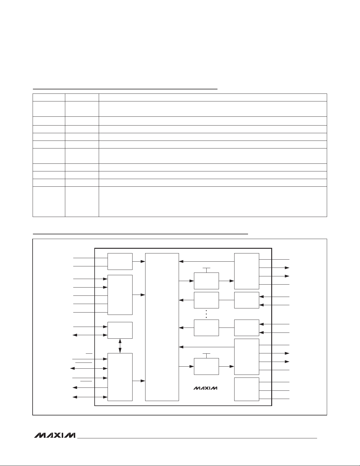
Functional Diagram
V
DD5
PGND
IN_+
IN-
V
GND
REF
SCL
SDA
CLO
MUTE_CL1
FLT_OT
SYNC
OSC
DD
EN
ANALOG
AUDIO
INTERFACE
I2C CONTROL
INTERFACE
REGISTERS
AND
SYSTEM
CONTROL
ANALOG
MODULATOR
AND
DIAGNOSTICS
V
DD5
GATE
DRIVER 0
LPF
LPF
V
DD5
GATE
DRIVER 3
MAX13301
CLASS D
OUTPUT
STAGE 0
AND DIAGS
FEEDBACK
DIFF. AMP
FEEDBACK
DIFF. AMP
CLASS D
OUTPUT
STAGE 3
AND DIAGS
CHARGE
PUMP
PVDD
OUT0+
OUT0-
PGND
FB0+
FB0-
FB3+
FB3-
PVDD
OUT3+
OUT3-
PGND
CP
CM
CHOLD
11
Page 12
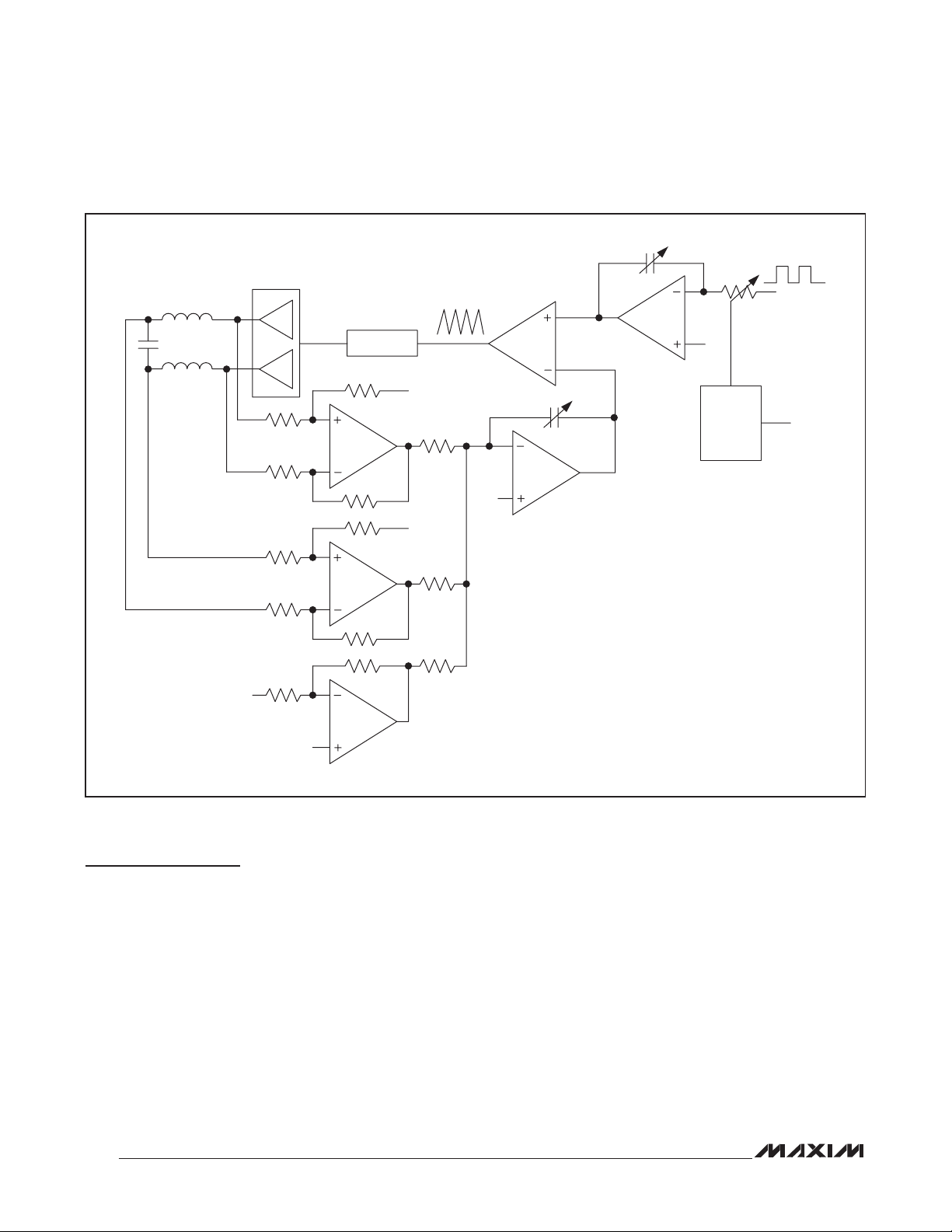
4-Channel, Automotive Class D Audio Amplifier
2
C COMP
I
MAX13301
AUDIO IN
PWM LOGIC
TRIANGLE WAVE
REF
REF
PWM
COMPARATOR
REF
I2C COMP
ERROR
AMPLIFIER
REF
3-BIT ADC
FEED-
FORWARD
OSC
PVDD
REF
PREAMPLIFIER
Figure 1. Detailed Block Diagram of the MAX13301 Audio Path
Detailed Description
The MAX13301 4-channel, Class D audio power amplifiers is specifically designed for automotive applications.
Integrated feedback from the LC filter’s output improves
the THD+N by reducing the distortion, providing Class
AB performance while achieving efficiency up to 90.5%.
The devices also support spread-spectrum modulation
for AM radio compatibility.
Description of Operation
The device emulates current-mode controllers with digital
feed-forward (Figure 1). The internal oscillator creates an
18MHz square wave. The I2C controls a clock divider that
divides down this high-frequency clock to a usable frequency. The resulting square wave is integrated to create
12
a triangle wave. A 3-bit ADC converts the PVDD voltage
into a code that adjusts the resistors used in the trianglewave integrator. The triangle-wave amplitude becomes
progressively larger as PVDD increases. The triangle
wave is fed into the PWM comparator.
The two differential amplifiers provide both analog and
digital feedback. The feedback is summed with the output of the preamplifier at the error amplifier. The output
of the error amplifier is an AC replica of the inductor current (emulated current mode) and the triangle wave is
therefore the slope compensation. The PWM comparator
controls the full-bridge operation, turning on and off each
FET pair (double-edge modulation). To ensure that the
devices switch at the desired frequency, it is important
to ensure that the triangle wave is greater than the error-
Page 13

4-Channel, Automotive Class D Audio Amplifier
amplifier ramp. The design equation that must be met to
ensure constant frequency is as follows:
Error-Amplifier Ramp < 2/3 Triangle-Wave Ramp
The error-amplifier ramp is fixed by the gain of the differential amplifiers used in the feedback loop and by
the error-amplifier compensation capacitor programmed
through I2C. To ensure the design equation for fixed frequency is met, the error-amplifier compensation capacitor tracks the integrator capacitor used to generate the
triangle wave.
For optimal noise shaping, the error-amplifier capacitor should be set to a small value. This results in a
broadband spectrum where the error amplifier pushes
the noise created by the clock jitter and PWM sampling above the audio range. However, there is a limit.
Because the triangle-wave capacitor tracks the erroramplifier capacitor, small capacitor values can clip
the triangle wave as it runs out of supply. This effect is
aggravated at high PVDD voltages by the ADC action
that decreases the integrator resistor at higher supply
voltages. Tables 20 and 21 are lookup tables to facilitate choosing the optimal setting for the error-amplifier
capacitance (MAP.COMP[2:0]).
It is possible to change this setting instantaneously while
playing music, but if there is no music, a slight audible
click is heard at the speakers. Systems that monitor
the input voltage can take advantage of this instantaneous programmability and use a smaller error-amplifier
capacitor at lower PVDD voltages. Higher switching
frequencies also allow the use of a smaller integrator
capacitor, and thus help improve the noise performance
of the amplifier.
Do not set the error-amplifier capacitor to a value less
than 18pF. Doing so results in extreme distortion, as the
triangle wave clips. The MAP.COMP[2:0] settings that
result in this behavior are listed as reserved (Table 19).
Advantage of Feedback After the Filter
High-fidelity audio amplifiers require very low output
impedance. The device achieves this by using a dual-
feedback approach. The digital feedback (feedback
MAX13301
from OUT__ outputs) emulates current-mode enabling on
chip compensation. The analog feedback (FB__ inputs)
significantly reduces the output impedance of the amplifier and at the same time, compensates for the nonideal
characteristics of the output filter. If the characteristics
of the speaker and/or output filter change with age or
temperature, the analog feedback compensates accordingly. Further inductor matching is less critical because
the inductors are inside the feedback loop. Because the
inductors are inside the feedback loop, the loop can
dampen out any LC ringing that might occur when the
amplifier is used as a line driver. The analog feedback is
differential so it does not help with common-mode ringing. Thus, the Zobel (RC) networks are required on each
speaker connection to damp any common-mode ringing
associated with the LC output filter and speaker.
Operating Modes
Configure the device for one of three states of activity:
normal, standby, or shutdown.
Normal
In normal mode, the device is ready for play. Placing
the device in standby reduces power consumption while
keeping fault monitors and the I2C interface on to communicate fault conditions. In shutdown, the device is
completely disabled and draws minimal current from the
battery.
To reset the device and clear all register contents to their
reset values, set CTRL5.RST to 1. After reset, this bit is
automatically cleared back to 0.
Standby
In standby, all circuitry is disabled except the fault monitors and the I2C interface. The I2C registers retain their
content and are still interactive. To place the device in
standby, set the CTRL2.STBY bit to 1. In standby, the
device draws 11mA from all power-supply inputs.
Before exiting standby, always set the CTRL1.CL_TH (current-limit threshold setting) bit to 1. After exiting standby,
clear CTRL1.CL_TH back to 0.
Table 1. Operating Modes
MODE EN CTRL2.STBY I2C FAULT MONITORS ALL OTHER CIRCUITRY
Normal High 0 Enabled On On
Standby High 1 Enabled On Off
Shutdown Low X Off Off Off
X = Don’t care
13
Page 14
4-Channel, Automotive Class D Audio Amplifier
Shutdown
In shutdown, all circuitry including the fault monitors and
I2C interface is disabled to reduce power consumption
and extend battery life. Connect EN to logic-high for normal operation. Connect EN to GND to place the device in a
low-power shutdown mode. In shutdown, the devices draw
17mA (typ) from the battery.
Clock Source
The device supports fixed-frequency modulation with an
MAX13301
internal or external clock. The modulation mode is selected through CTRL1.CM[1:0] (operating mode select bits).
Master Configuration
In master mode, 10 modulation frequencies are available in fixed-frequency modulation mode. Program
CTRL0.MDIV[3:0] (master clock-divide ratio bits) for the
desired frequency.
Slave Configuration
Configuring the device as a slave allows an external
clock source to provide the switching frequency. In this
case, apply the external clock signal at SYNC at double
the desired switching frequency.
Fixed-Frequency Modulation Mode
The devices supports a fixed-frequency modulation
mode with 10 different selectable frequencies between
300kHz and 750kHz. The frequency is selectable through
the I2C interface. The frequency spectrum consists of the
fundamental switching frequency and its associated
harmonics (see the wideband output spectrum graphs in
the Typical Operating Characteristics). For applications
where exact spectrum placement of the switching fundamental is important, program the switching frequency so
that the harmonics do not fall within a sensitive frequency
band.
Spread Spectrum
The device features a unique spread-sprectrum mode
that flattens the wideband spectral components, improving EMI emissions that can be radiated by the speaker
and cables. This feature is only available in master clock
mode and is enabled by setting the CTRL5.SS[2:0] and
CTRL5.SSEN bits. In spread-spectrum mode, the switching frequency vaies linearly by up to 7% depending on
CTRL5.SS[2:0] setting. The modulation scheme remains
the same, but the period of the triangle waveform
changes from cycle to cycle. Instead of a large amount
of spectral energy present at multiples of the switching
frequency, the energy is now spread over a bandwidth
that increases with frequency. Above a few megahertz,
the wideband spectrum looks like white noise for EMI
purposes. A proprietary amplifier topology ensures this
does not significantly increase the noise floor in the
audio bandwidth.
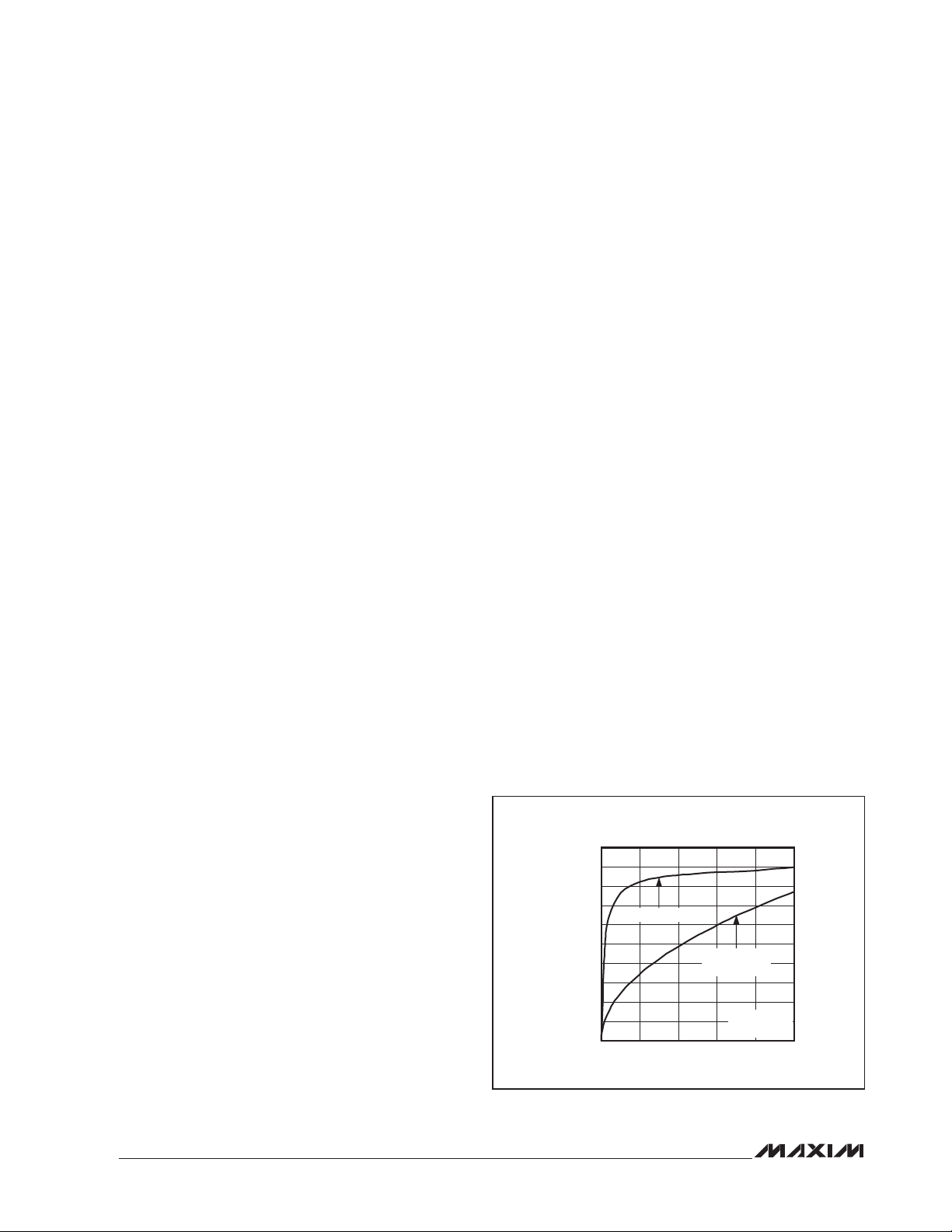
Efficiency
The high efficiency of a Class D amplifier is due to the
switching operation of the output stage transistors. In a
Class D amplifier, the output transistors act as currentsteering switches and consume negligible additional
power. Any power loss associated with the Class D
output stage is mostly due to the I2R loss of the MOSFET
on-resistance and quiescent current overhead. The
theoretical best efficiency of a linear amplifier is 78% at
peak output power. Under normal operating levels (typical music reproduction levels), the efficiency falls below
30%, whereas the device exhibits > 80% efficiency
under the same conditions (Figure 2).
Current Limit
The current limit of the outputs is selectable between 7A
(typ) and 8.75A (typ) through the CTRL3.HCL bit.
When the current limit is exceeded, the affected output
is latched off and its corresponding overcurrent indicator bit OSTAT0.OC[3:0] is set to 0. The device does
not attempt to activate the output until instructed by
the microcontroller to do so. After eliminating the cause
of the current limit, reactivate the output by setting
OSTAT0.OC[3:0] to 1.
Short to either ground or battery causes the output to be
latched off and its corresponding OSTAT0.OC[3:0] bit
to be set to 0. After removing the short, reactivate the
output by setting OSTAT0.OC[3:0] to 1.
MAX13301 EFFICIENCY vs.
IDEAL CLASS AB AMPLIFIER EFFICIENCY
100
90
80
70
60
50
40
EFFICIENCY (%)
30
20
10
0
Figure 2. Efficiency vs. Output Power of Class AB Amplifier
and the MAX13301
MAX13301
IDEAL CLASS AB
AMPLIFIER
V
= 14.4V
PVDD
RL = 4I
0 25
OUTPUT POWER PER CHANNEL (W)
2015105
14
Page 15

4-Channel, Automotive Class D Audio Amplifier
The device has real-time current limit for shorted outputs,
outputs shorted to battery, outputs shorted to ground,
and outputs shorted to adjacent channels.
For shorted outputs, the devices enter cycle-by-cycle
current limit. In a BTL configuration, current flows
diagonally through two of the four FETs at any instant
in time. If the current in either of these FETs reaches
the current-limit threshold, then both turn off and the
other pair of diagonal FETs turns on for a fixed time.
This creates distortion, as the music clips. The internal
logic of the device counts the cycle-by-cycle currentlimit events, and if too many happen in a fixed amount
of time, the devices latch off the faulted channel. Current
limit is programmable with the I2C. When CTRL3.HCL
= 1, the peak current is limited to 8.75A (typ). With
CTRL3.HCL = 0, peak current is limited to 7A (typ).
Short-to-battery and short-to-ground take advantage
of the diagonal flow of current in a full bridge to detect
fault conditions. The load current during normal operation should be equal in the two diagonal FETs that are
actively conducting current. When an output is shorted
to battery or ground, the current is no longer equal and
the degree of mismatch is a measure of the severity of
the fault. If the mismatch threshold is exceeded in any
channel, that channel is immediately shut down and an
overcurrent fault is reported. The level of mismatch is
programmable through I2C. When CTRL1.CL_TH = 0,
the mismatch threshold is 3.09A with CTRL3.HCL = 0 and
3.86A with CTRL3.HCL = 1. When CTRL1.CL_TH = 1, the
mismatch threshold is 1.03A with CTRL3.HCL = 0 and
1.28A with CTRL3.HCL = 1. The lower setting is preferred in that it can detect a misconfigured speaker. For
example, the lower setting issues a fault if a 4I speaker
is incorrectly connected between one of the outputs
and ground. At startup, when a large snubber capacitor
is present, the higher setting is sometimes required to
avoid false trips. When the bridge starts switching, both
snubber capacitors must be charged to half the battery.
The charging current mimics a short to ground. Following
the startup procedure is the best way to avoid issues
with overcurrent faults.
Mute/Precharging
The device features a clickless/popless mute mode.
When muted, the volume at the speaker is reduced to an
inaudible level. To mute the device, configure MUTE_CL1
as a mute input by setting MAP.MCLP (clip output mapping bit) to 0. Then drive the mute input low. Use the mute
function during system power-up and power-down to
ensure optimum click-and-pop performance.
It is also advisable to set CTRL1.PRE (precharge bit) to
1 after taking the device out of standby mode to precharge the input DC-blocking capacitors. This action
should be part of any startup routine. Precharging the
DC-blocking capacitors enhances click-and-pop performance. Capacitors that are 0.47µF/2µF in series with the
inputs take about 1ms to be charged.
Output Configuration
The four FETs forming the full-bridge output of each
channel can be programmed into one of four states:
high-impedance (default), forced overvoltage, mute, and
play through the CTRL2.MD01_[1:0] (channels 0 and 1
output mode) and CTRL2.MD23_[1:0] (channels 2 and
3 output mode) bits. Channels 0 and 1 and channels 2
and 3 always share the same configuration.
In high-impedance mode, all four FETs are turned off. In
forced overvoltage state, each half-bridge output is regulated to 1/2 V
to switch but the volume is kept to an inaudible level. In
play mode, the FETs switch normally.
. In mute mode, the outputs continue
PVDD
I2C Interface
The device features an I2C, 2-wire serial interface consisting of a serial-data line (SDA) and a serial-clock line
(SCL). SDA and SCL facilitate communication between
the device and the master at clock rates up to 400kHz.
When the device is used on an I2C bus with multiple
devices, the VDD supply must stay powered on to ensure
proper I2C bus operation. The master, typically a microcontroller, generates SCL and initiates data transfer
on the bus. Figure 3 shows the 2-wire interface timing
diagram.
A master device communicates to the IC by transmitting
the proper address followed by the data word. Each
transmit sequence is framed by a START (S) or repeated
START (Sr) condition, and a STOP (P) condition. Each
word transmitted over the bus is 8 bits long and is always
followed by an acknowledge clock pulse.
The SDA line operates as both an input and an opendrain output. A pullup resistor, greater than 500I, is
required on the SDA bus. The SCL line operates as
an input only. A pullup resistor, greater than 500I, is
required on SCL if there are multiple masters on the bus,
or if the master in a single-master system has an opendrain SCL output. Series resistors in line with SDA and
SCL are optional. The SCL and SDA inputs suppress
noise spikes to ensure proper device operation even on
a noisy bus.
MAX13301
15
Page 16

4-Channel, Automotive Class D Audio Amplifier
SDA
t
t
SU:DAT
t
HD:DAT
t
F
SCL
MAX13301
t
HD:STA
START
CONDITION
t
LOW
t
HIGH
t
R
Figure 3. 2-Wire Serial-Interface Timing Diagram
S PSr
SDA
SCL
Figure 4. START, STOP, and Repeated START Conditions
Bit Transfer
One data bit is transferred during each SCL cycle. The
data on SDA must remain stable during the high period
of the SCL pulse. Changes in SDA while SCL is high are
control signals (see the START and STOP Conditions sec-
tion). SDA and SCL idle high when the I2C bus is not busy.
STOP and START Conditions
A master device initiates communication by issuing a
START condition. A START condition is a high-to-low
transition on SDA with SCL high. A STOP condition is a
low-to-high transition on SDA while SCL is high (Figure 4).
A START condition from the master signals the beginning
of a transmission to the device. The master terminates
transmission and frees the bus by issuing a STOP condition. The bus remains active if a repeated START condition is generated instead of a STOP condition.
t
SU:STA
REPEATED
CONDITION
START
t
HD:STA
t
SP
t
SU:STO
CONDITION
Early STOP Condition
The device recognizes a STOP condition at any point during data transmission, except if the STOP condition occurs
in the same high pulse as a START condition.
Each time the device is enabled, the state of the
MUTE_CL1 input is latched and determines the device’s
slave address. Table 2 shows the two possible hardware-defined slave addresses of the devices.
Once the device is enabled, it is programmable to one of
four I2C slave addresses through CTRL4.ADDR[1:0] (I2C
slave address setting bits), as shown in Table 3. When
initially setting the slave address, use the default slave
address as discussed in the previous paragraph and
shown in Table 2. After setting the slave address, set the
CTRL5.ADDR_DEF (I2C slave address definition bit) to 1.
For subsequent reads and writes, use the new softwaredefined address. These slave addresses are unique
device IDs.
The address is defined as the 7 most significant bits
(MSBs) followed by the R/W bit. Set the R/W bit to 1 to
configure the device to read mode. Set the R/W bit to 0
to configure the device to write mode. The address is
the first byte of information sent to the device after the
START condition.
BUF
STOP
CONDITION
Slave Address
START
16
Page 17

4-Channel, Automotive Class D Audio Amplifier
Table 2. Default Slave Address
MUTE_CL1
Low 1 1 0 1 1 0 1 X 0xDA 0xDB
High 1 1 0 1 1 0 0 X 0xD8 0xD9
A6 A5 A4 A3 A2 A1 A0
R/W
Table 3. I2C Programmable Slave Address
CTRL4.
ADDR[1:0]
00 1 1 0 1 1 0 0 X 0xD8 0xD9
01 1 1 0 1 1 1 0 X 0xDC 0xDD
10 1 1 0 1 1 0 1 X 0xDA 0xDB
11 1 1 0 1 1 1 1 X 0xDE 0xDF
A6 A5 A4 A3 A2 A1 A0
R/W
WRITE READ
WRITE READ
MAX13301
Acknowledge
The acknowledge bit (ACK) is a clocked 9th bit that the
device uses to handshake receipt each byte of data
(Figure 5). The device pulls down SDA during the master-generated 9th clock pulse. The SDA line must remain
stable and low during the high period of the acknowledge clock pulse. Monitoring ACK allows for detection
of unsuccessful data transfers. An unsuccessful data
transfer occurs if a receiving device is busy or if a system
fault has occurred. In the event of an unsuccessful data
transfer, the bus master can reattempt communication.
S
SDA
SCL
Figure 5. Acknowledge Condition
1 2 8 9
Write Data Format
A write to the device includes transmission of a START condition, the slave address with the write bit set to 0, one byte
of data to register address, one byte of data to the command register, and a STOP condition. Figure 6 illustrates
the proper format for one frame.
Read Data Format
A read from the device includes transmission of a START
condition, the slave address with the write bit set to 0, one
byte of data to register address, restart condition, the slave
address with read bit set to 1, one byte of data to the command register, and a STOP condition. Figure 6 illustrates
the proper format for one frame.
ACKNOWLEDGE
SLAVE ADDRESS
S A A P
(WRITE ADDRESS)
SLAVE ADDRESS
S A A Sr
(WRITE ADDRESS)
S = START CONDITION, A = ACKNOWLEDGE, NA = NOT ACKNOWLEDGE
Sr = REPEATED START CONDITION, P = STOP CONDITION
Figure 6. Data Format of I2C Interface Write Mode Read Mode
REGISTER
ADDRESS
REGISTER
ADDRESS
DATA
SLAVE ADDRESS
(READ ADDRESS)
A
A DATA NA
P
17
Page 18

4-Channel, Automotive Class D Audio Amplifier
Register Map
Table 4. Register Map
REGISTER BIT 7 BIT 6 BIT 5 BIT 4 BIT 3 BIT 2 BIT 1 BIT 0 ADDRESS R/W
CTRL0 — — MDIV3 MDIV2 MDIV1 MDIV0 TW1 TW0 0x00 R/W 0x24
CTRL1 — CL_TH CLVL1 CLVL0 — PRE CM1 CM0 0x01 R/W 0x00
CTRL2 — — STBY — MD23_1 MD23_0 MD01_1 MD01_0 0x02 R/W 0x20
CTRL3 TW RDET SDET DIS — HCL — LDM 0x03 R/W 0x00
MAX13301
CTRL4 — — ADDR1 ADDR0 — — — — 0x04 R/W 0xC0
CTRL5 SSEN RST SS2 SS1 SS0 PAR1 PAR0 ADDR_DEF 0x05 R/W 0x01
MAP COMP2 COMP1 COMP0 OTWM LCTM MCLP OTM FLTM 0x06 R/W 0x40
STAT —
OSTAT0
OSTAT1
OSTAT2
OSTAT3 — — — VER
OC3 OC2 OC1 OC0 CLIP3 CLIP2 CLIP1 CLIP0
LDOK3 LDOK2 LDOK1 LDOK0 LOAD3 LOAD2 LOAD1 LOAD0
SBAT3 SBAT2 SBAT1 SBAT0 SGND3 SGND2 SGND1 SGND0
OT OTW OV UV OC CPUV CLIP
VOS3 VOS2 VOS1 VOS0
0x07 R —
0x08 R —
0x09 R —
0x0A R —
0x0B R —
Table 5. Control Register 0
CTRL0
BIT # 7 6 5 4 3 2 1 0
NAME
POR
— — MDIV3 MDIV2 MDIV1 MDIV0 TW1 TW0
0 0 1 0 0 1 0 0
POWER-ON
RESET (POR)
Table 6. Control Register 0 Bit Description
BIT BIT DESCRIPTION
Master Clock-Divide Ratio. In master mode, the modulation and charge-pump frequencies are each set
to 4.5MHz/(MDIV[3:0]). The device is in standby mode for MDIV[3:0] ≤ 3. The valid operating frequencies
are 750kHz, 642.9kHz, 562.5kHz, 500kHz, 450kHz, 409.1kHz, 375kHz, 346.2kHz, 321.4kHz, and 300kHz.
MDIV[3:0]
TW[1:0]
18
Switching frequencies below 450kHz compromises noise, as a larger integrator and triangle-wave capacitor
trim setting is required.
In slave mode, the modulation and charge-pump frequency are always set to f
frequency of the clock signal applied to the SYNC input.
Thermal Warning Threshold. This threshold determines the temperature at which the status bit STAT.OTW
asserts.
00 = Junction temperature exceeds 110NC.
01 = Junction temperature exceeds 120NC.
10 = Junction temperature exceeds 130NC.
11 = Junction temperature exceeds 140NC.
SYNC
/2, where f
SYNC
is the
Page 19

4-Channel, Automotive Class D Audio Amplifier
Table 7. Control Register 1
CTRL1
BIT # 7 6 5 4 3 2 1 0
NAME
POR
Table 8. Control Register 1 Bit Description
BIT BIT DESCRIPTION
CL_TH
CLVL[1:0]
PRE
CM[1:0]
— CL_TH CLVL1 CLVL0 — PRE CM1 CM0
0 0 0 0 0 0 0 0
Selects the current threshold for the real-time short-to-ground and short-to-battery detection diagnostics.
Set this bit to 0 before exiting high-Z mode to prevent false triggering of short-to-ground and short-to-battery
faults during startup. Set this bit to 1 after the device has entered mute or play mode.
0 = High threshold
1 = Normal threshold
Clip Level. The clip level provides an indication of the amount of total harmonic distortion in the output signal.
00 = THD exceeds 10%
10 = THD exceeds 5%
01 = THD exceeds 3%
11 = THD exceeds 1%
Precharge. Use PRE to precharge the input DC-blocking capacitors. Set this bit to 1 as part of the startup
procedure. A 2FF capacitor for IN- and 0.47FF input blocking capacitors require a 1ms precharge to avoid
startup pop.
0 = Disable precharging
1 = Enable precharging
Clock Mode. Before selecting the operating mode, three-state all outputs.
00 = Master fixed frequency, switching frequency set by the master clock-divide ratio (CTRL0.MDIV[3:0])
bits, SYNC output disabled
01 = Master fixed frequency, switching frequency set by the master clock-divide ratio (CTRL0.MDIV[3:0])
bits, SYNC output enabled
10 = Reserved
11 = Slave fixed frequency, SYNC input enabled
MAX13301
19
Page 20

4-Channel, Automotive Class D Audio Amplifier
Table 9. Control Register 2
CTRL2
BIT # 7 6 5 4 3 2 1 0
NAME
POR
Table 10. Control Register 2 Bit Description
MAX13301
BIT BIT DESCRIPTION
STBY
MD23_[1:0]
MD01_[1:0]
— — STBY — MD23_1 MD23_0 MD01_1 MD01_0
0 0 1 0 0 0 0 0
Standby Mode. Wait 50ms after exiting standby mode to allow the charge pump and reference to stabilize
before entering mute or play mode.
0 = Normal mode
1 = Standby mode. The charge pump, preamplifier, and modulator are disabled. Fault monitors and I2C are
still active.
Channels 2 and 3 Output Mode. Channels 2 and 3 are always in the same configuration. MD23_[1:0]
determines the state of outputs 2 and 3.
00 = High-Z
01 = Mute
10 = Forced overvoltage. In this state, both differential outputs are charged to 1/2 V
11 = Play
Channels 0 and 1 Output Mode. Channels 0 and 1 are always in the same mode. MD01_[1:0] determines
the state of outputs 0 and 1.
00 = High-Z
01 = Mute
10 = Force overvoltage. In this state, both differential outputs are charged to 1/2 V
11 = Play
PVDD
PVDD
.
.
20
Page 21

4-Channel, Automotive Class D Audio Amplifier
Table 11. Control Register 3
CTRL3
BIT # 7 6 5 4 3 2 1 0
NAME
POR
Table 12. Control Register 3 Bit Description
BIT BIT DESCRIPTION
TW
RDET
TW RDET SDET DIS — HCL — LDM
0 0 0 0 0 0 0 0
Tweeter-Detect Current Threshold Setting
0 = The current threshold at which OSTAT1.LOAD[3:0] (load indicator bit) asserts is set equal to the shortedload current threshold (see the Electrical Characteristics table). Use this setting when running shorted-load
diagnostic.
1 = The current threshold at which OSTAT1.LOAD[3:0] asserts is set equal to the tweeter detect current
threshold. This threshold is approximately 25% of the default value to facilitate tweeter detection. Use this
setting when the running tweeter diagnostic or for detecting the presence of a speaker.
Open-Load Diagnostic Enable. Upon detecting an open load on any of the outputs, the corresponding
OSTAT1.LDOK[3:0] (load OK indicator bit) asserts. Always perform short-to-ground and short-to-battery
diagnosis before entering RDET mode. If a short-to-battery is detected, do not enter RDET mode. After
performing the short-to-battery test, discharge both outputs by setting CTRL3.DIS to 1 for 200µs, then reset
CTRL3.DIS back to 0. Failure to follow this procedure can result in a loud pop at the speaker.
Because the results are not latched, read LDOK[3:0] before clearing RDET. Wait a minimum of 200µs before
reading these status bits. RDET can only be set after three-stating all four outputs. When performing the
open-load diagnostic, set the CTRL3.SDET (short-to-ground/battery enable) bit to 0.
0 = Disable open-load diagnostic
1 = Enable open-load diagnostic
MAX13301
SDET
DIS
HCL
LDM
Short-to-Ground/Battery Diagnostic Enable. Upon detecting a short-to-ground or battery on any of the outputs,
the corresponding OSTAT2.SBAT[3:0] (short-to-battery) and OSTAT2.SGND[3:0] (short-to-ground) bits assert.
Because the results are not latched, read OSTAT2.SBAT[3:0] and OSTAT2.SGND[3:0] before clearing SDET.
Wait a minimum of 200µs before reading these status bits. Before setting SDET to 1, three-state all four outputs and set the CTRL3.DIS (discharge output enable) bit to 1 and then reset back to 0. Before performing
the short-to-ground/battery diagnostic, set the CTRL3.RDET (open-load diagnostic enable) bit to 0. To test for
short-to-ground, set CTRL2.STBY to 0, and to test for short-to-battery, set CTRL2.STBY to 1.
0 = Disable short-to-ground/battery diagnostic
1 = Enable short-to-ground/battery diagnostic
Discharge Output Enable. Set DIS to 1 to discharge all outputs with 15mA current sources. Use DIS to discharge all outputs before performing the short-to-ground/battery diagnostic (SDET) to avoid a loud pop on
the speaker. DIS can only be set to 1 after three-stating all four outputs.
0 = Output discharge is disabled.
1 = Output discharge is enabled.
Current-Limit Level. HCL sets the current-limit threshold of the outputs during normal operation.
0 = 7A (typ) current limit
1 = 8.75A (typ) current limit
Line-Driver Mode. Use LDM to set the load resistance threshold required to assert the OSTAT1.LDOK[3:0]
(load-okay indicator bit). Any load with a resistance greater than the threshold is interpreted as an open
output.
0 = Line-driver mode, OSTAT1.LDOK[3:0] = 1 if RL > 300I
1 = Power amplifier mode, OSTAT1.LDOK[3:0] = 1 if RL > 100I
21
Page 22

4-Channel, Automotive Class D Audio Amplifier
Table 13. Control Register 4
CTRL4
BIT # 7 6 5 4 3 2 1 0
NAME
POR
Table 14. Control Register 4 Bit Description
MAX13301
BIT BIT DESCRIPTION
ADDR[1:0]
— — ADDR1 ADDR0 — — — —
1 1 0 0 X X X X
I2C Slave Address Setting. Use ADDR[1:0] to set the slave address of the device. After setting the slave
address, set CTRL5.ADDR_DEF (I2C slave address definition bit) to 1 to make the new address effective.
00 = Slave address set to 1101100 R/W
01 = Slave address set to 1101110 R/W
10 = Slave address set to 1101101 R/W
11 = Slave address set to 1101111 R/W
22
Page 23

4-Channel, Automotive Class D Audio Amplifier
Table 15. Control Register 5
CTRL5
BIT # 7 6 5 4 3 2 1 0
NAME
POR
Table 16. Control Register 5 Bit Description
BIT BIT DESCRIPTION
SSEN
RST
SS[2:0]
PAR[1:0]
SSEN RST SS2 SS1 SS0 PAR1 PAR0 ADDR_DEF
0 0 0 0 0 0 0 1
Spread-Spectrum Modulation Enable.
0: Spread-spectrum disabled; SSEN = 1 and SS[2:0] > 0: Spread-spectrum enabled
Reset. Setting RST to 1 resets the device. In reset, all register bits are reset to their POR values. RST is automatically cleared back to 0 after device reset.
0 = Not in reset
1 = Reset
Spread-Spectrum Modulation Control. Spread-spectrum modulation is enabled when SSEN = 1 and SS[2:0]
> 0, once enabled the switching frequency varies from +2% to +7% (see Table 17).
Parallel Mode. The four outputs can be paralleled in one of four ways. To parallel outputs, connect the positive outputs together and connect the negative outputs together. In parallel mode, only the feedback inputs
corresponding to the slaved input IN0+ or IN2+ are used. Connect the other feedback inputs to ground.
00 = 4-channel output
01 = 2.1-channel output. Outputs 0 and 1 are paralleled and slaved to input IN0+. Channels 2 and 3 are
unaffected.
10 = 2.1-channel output. Outputs 2 and 3 are paralleled and slaved to input IN2+. Channels 0 and 1 are
unaffected.
11 = 2-channel output. Outputs 0 and 1 are paralleled and slaved to input IN0+. Outputs 2 and 3 are paralleled and slaved to input IN2+.
MAX13301
I2C Slave Address Definition. This bit determines whether the I2C slave address is hardware or softwaredefined.
ADDR_DEF
0 = Slave address is defined by CTRL4.ADDR[1:0] (I2C slave address setting bits).
1 = Slave address is set to the default address as defined by the state of the MUTE_CL1 input when the
enable input EN is pulled high.
Table 17. Spread-Spectrum Modulation Table
SSEN SS2 SS1 SS0 SPREAD (%)
0 X X X Disabled
1 0 0 0 0
1 0 0 1 2
1 0 1 0 3
1 0 1 1 4
1 1 0 0 5
1 1 0 1 6
1 1 1 0 7
1 1 1 1 Reserved
23
Page 24

4-Channel, Automotive Class D Audio Amplifier
Table 18. Mapping Register
MAP
BIT # 7 6 5 4 3 2 1 0
NAME
POR
Table 19. Mapping Register Bit Description
MAX13301
BIT BIT DESCRIPTION
COMP[2:0]
OTWM
LCTM
MCLP
OTM
FLTM
COMP2 COMP1 COMP0 OTWM LCTM MCLP OTM FLTM
0 1 0 0 0 0 0 0
Integrator and Triangle-Wave Capacitor Trim. A smaller integrator capacitor pushes noise out of the audio
band yielding the lowest noise. If distortion rises at high output powers, lower switching frequencies, or
higher PVDD voltages then use a larger capacitor setting. See Table 20 for choosing minimum capacitor
settings based on PVDD and the switching frequency. Larger capacitor values can be used.
If all 4 channels of the amplifier are used to drive subwoofers, the capacitor settings can be relaxed
because a smaller capacitor setting helps to eliminate high-frequency noise (greater than 10kHz). Systems
with multiple tweeters benefit the most from proper COMP[2:0] selection. Lower switching frequencies are
possible when this high-frequency noise is not a concern as with systems that lack tweeters.
000 = 43pF
001 = 37pF
010 = 31pF
011 = 25pF
100 = 18pF
101 = Reserved
110 = Reserved
111 = Reserved
Overtemperature Warning Mapping Bit
0 = STAT.OTW (overtemperature warning bit) is unmapped to the FLT_OT open-drain output.
1 = STAT.OTW is mapped to FLT_OT when MAP.OTM = 1.
Low-Current Threshold Mapping Bit. The current thresholds used in tweeter and shorted load diagnostics
are lower than the current limit. When the threshold is exceeded in running either diagnostic,
OSTAT1.LOAD[3:0] (load indicator bit) asserts. Hardware indication is also possible by using LCTM to map
OSTAT1.LOAD[3:0] to the CL0 and MUTE_CL1 outputs.
0 = OSTAT1.LOAD[3:0] (load indicator bit used for tweeter and shorted load diagnostics) is unmapped to
the CL0 and MUTE_CL1 outputs.
1 = OSTAT1.LOAD[3:0] is mapped to the CL0 and MUTE_CL1 outputs. Use this setting only when running
tweeter or shorted load diagnostic.
Clip Output Mapping. MCLP determines which open-drain outputs (CL0 and MUTE_CL1) are used to indicate clipping on an audio output. CL0 is always used as a clip indicator, while MUTE_CL1 is configurable
as a clip indicator output or as a mute input.
0 = CL0 provides clip indication for all audio outputs; MUTE_CL1 is configured as a mute input.
1 = CL0 provides clip indication for audio outputs 0 and 1; MUTE_CL1 is configured as a clip indicator output for audio outputs 2 and 3.
Overtemperature Shutdown Map
0 = STAT.OT (overtemperature shutdown bit) is unmapped to the open-drain FLT_OT output.
1 = STAT.OT is mapped to the FLT_OT output.
Fault Mapping Bit
0 = Faults are unmapped to the open-drain FLT_OT output.
1 = Any fault condition (as indicated by the status bits OV, UV, OC) causes FLT_OT to assert low.
24
Page 25

4-Channel, Automotive Class D Audio Amplifier
Table 20. COMP[2:0] Setting Lookup Table
fSW/V
PVDD
300k 100 100 100 011 011 010 001
320k 100 100 100 011 011 010 010
346k 100 100 100 100 011 010 010
375k 100 100 100 100 011 011 010
409k 100 100 100 100 100 011 011
450k 100 100 100 100 100 011 011
475k 100 100 100 100 100 100 011
500k 100 100 100 100 100 100 011
530k 100 100 100 100 100 100 011
562k 100 100 100 100 100 100 100
600k 100 100 100 100 100 100 100
643k 100 100 100 100 100 100 100
675k 100 100 100 100 100 100 100
700k 100 100 100 100 100 100 100
725k 100 100 100 100 100 100 100
750k 100 100 100 100 100 100 100
< 8V
8V to
9.5V
9.5V to
12.65V
12.65V to
15.6V
15.6V to
18.65V
18.65V to
21.1V
> 21.1V
MAX13301
Table 21. Status Register
STAT
BIT # 7 6 5 4 3 2 1 0
NAME
—
OT OTW OV UV OC CPUV CLIP
Table 22. Status Register Bit Description
BIT BIT DESCRIPTION
Overtemperature Shutdown. The device goes into thermal shutdown when the junction temperature exceeds
OT
OTW
OV
UV
+150NC.
0 = Device is in thermal shutdown.
1 = Device is not in thermal shutdown.
Overtemperature Warning. OTW asserts when the junction temperature exceeds the thermal warning threshold programmed in CTRL0.TW[1:0].
0 = Junction temperature is greater than the programmed thermal warning threshold.
1 = Junction temperature is less than the programmed thermal warning threshold.
Overvoltage Indicator
0 = V
Characteristics table.
1 = V
Undervoltage Indicator
0 = V
Characteristics table.
1 = V
is greater than the PVDD overvoltage lockout (OVLO) threshold as defined in the Electrical
PVDD
is less than the OVLO threshold.
PVDD
is less than the PVDD undervoltage lockout (UVLO) threshold as defined in the Electrical
PVDD
is greater than the UVLO threshold.
PVDD
25
Page 26

4-Channel, Automotive Class D Audio Amplifier
Table 22. Status Register Bit Description (continued)
BIT BIT DESCRIPTION
General Overcurrent Indicator. OC asserts when there is an overcurrent condition on any of the outputs
such as a short-to-ground/battery. To identify which output(s) is experiencing an overcurrent condition, read
OC
MAX13301
CPUV
CLIP
Table 23. Status Register 0
BIT # 7 6 5 4 3 2 1 0
NAME
the OSTAT0.OC[3:0] (overcurrent indicator bit).
0 = An overcurrent condition exists on one or more of the outputs.
1 = No overcurrent condition.
Charge-Pump Undervoltage Indicator. CPUV asserts when the voltage on the hold capacitor of the charge
pump (C
0 = Undervoltage on C
1 = Adequate voltage on C
General Clip Indicator. CLIP asserts when any of the outputs is clipping. To identify which output(s) is clipping, read the OSTAT0.CLIP[3:0] (clip indicator) bits.
0 = One or more outputs are clipping.
1 = None of the outputs are clipping.
OC3 OC2 OC1 OC0 CLIP3 CLIP2 CLIP1 CLIP0
) falls below 3.87V. It deasserts once the voltage rises above 4.1V.
HOLD
HOLD
HOLD
OSTAT0
Table 24. Status Register 0 Bit Description
BIT BIT DESCRIPTION
Overcurrent Indicator. An overcurrent condition such as a short-to-ground/battery on any of the outputs
causes the corresponding OC[3:0] bit to latch to 0. Write a 1 to this bit to clear it. Reset also clears this bit.
OC[3:0]
CLIP[3:0]
An overcurrent indicator is available for each output: OC3 is for output 3, OC2 is for output 2, etc.
0 = There is an overcurrent condition on the output.
1 = There is no overcurrent condition on the output.
Clip Indicator. CLIP[3:0] is a real-time clip indicator for each output. This bit asserts only during the times
when an overdriven output is actually clipping. A clip indictor is available for each output: CLIP3 is for output
3, CLIP2 is for output 2, etc.
0 = Output is clipping.
1 = Output is not clipping.
26
Page 27

4-Channel, Automotive Class D Audio Amplifier
Table 25. Status Register 1
OSTAT1
BIT # 7 6 5 4 3 2 1 0
NAME
Table 26. Status Register 1 Bit Description
LDOK[3:0]
LOAD[3:0]
LDOK3 LDOK2 LDOK1 LDOK0 LOAD3 LOAD2 LOAD1 LOAD0
BIT BIT DESCRIPTION
Load Okay Indicator. When running the open-load diagnostic, LDOK[3:0] = 1 if the load resistance
is greater than the resistance threshold set by CTRL3.LDM (line driver mode bit), indicating that the
output is properly loaded and not open. A load okay indicator is available for each output: LDOK3 is
for output 3, LDOK2 is for output 2, etc.
0 = Output is loaded.
1 = Output is open.
Load Indicator. When running shorted load or tweeter diagnostic, LOAD[3:0] asserts if there is a
short across the load or if a tweeter is connected. See the Shorted-Load Diagnostic and Tweeter
Diagnostic sections for information on the use of LOAD[3:0] in performing load diagnostics.
LOAD[3:0] is available for each output: LOAD3 is for output 3, LOAD2 is for output 2, etc.
0 = Load threshold exceeded.
1 = Load threshold not exceeded.
MAX13301
Table 27. Status Register 2
OSTAT2
BIT # 7 6 5 4 3 2 1 0
NAME
SBAT3 SBAT2 SBAT1 SBAT0 SGND3 SGND2 SGND1 SGND0
Table 28. Status Register 2 Bit Description
BIT BIT DESCRIPTION
Short-to-Battery Indicator. When running a short-to-ground/battery diagnostic, SBAT[3:0] provides indication of any short-to-battery for each output. Use SBAT[3:0] to ensure that there is no short-to-battery before
SBAT[3:0]
SGND[3:0]
turning on the device. This indicator is available for each output: SBAT3 is for output 3, SBAT2 is for output
2, etc.
0 = Output is shorted to the battery.
1 = Output is not shorted to the battery.
Short-to-Ground Indicator. When running a short-to-ground/battery diagnostic, SGND[3:0] provides indication of any short-to-ground for each output. Use SGND[3:0] to ensure that there is no short-to-ground
before turning on the device. This indicator is available for each output: SGND3 is for output 3, SGND2 is
for output 2, etc.
0 = Output is shorted to ground.
1 = Output is not shorted to ground.
27
Page 28

4-Channel, Automotive Class D Audio Amplifier
Table 29. Status Register 3
OSTAT3
BIT # 7 6 5 4 3 2 1 0
NAME
Table 30. Status Register 3 Bit Description
BIT BIT DESCRIPTION
MAX13301
VER
VOS[3:0]
Table 31. Fault Conditions
Overvoltage All
Undervoltage (PVDD) Normal, Standby
Charge-Pump Undervoltage Normal I2C High-Z All No
Overtemperature Shutdown Normal, Standby
Overtemperature Warning Normal
Open Load Normal I2C None No
Shorted Load Normal I2C High-Z Channel Yes
Short-to-Ground/Battery Normal
Clip Output Normal
Overcurrent Normal
DC Offset Normal, No Music I2C None No
— — — VER
Version Indicator.
0 = Reserved
1 = MAX13301
Offset Voltage Indicator. VOS[3:0] indicates whether an offset voltage exists between the differential outputs.
Read this bit in play mode after precharge with no signal on the input. This bit is not latched and is not a
valid indicator of offset when an input signal is present. An offset voltage indicator is available for each output: VOS3 is for output 3, VOS2 is for output 2, etc.
0 = The differential offset voltage between OUT_+ and OUT_- exceeds Q1V (typ).
1 = The differential offset voltage between OUT_+ and OUT_- is within Q1V (typ).
FAULT MONITORING STATE REPORTING METHOD ACTION LATCHED
I2C, CL0, MUTE_CL1
VOS3 VOS2 VOS1 VOS0
I2C, FLT_OT
I2C, FLT_OT
I2C, FLT_OT
I2C, FLT_OT
I2C, FLT_OT
I2C, FLT_OT
OUT_ to 1/2 V
High-Z All No
High-Z All No
High-Z Channel Yes
High-Z Channel Yes
PVDD
None No
None No
No
Fault Detection
The device integrates fault detection and protection
circuitry. Table 31 lists all fault events that each device
can encounter, the modes in which they are detected,
the method with which they are reported, the devices'
response to them, and whether they cause the outputs
to latch into a high-impedance state.
Load Diagnostics
The device incorporates built-in diagnostics to detect
external wire harness faults that can occur during installation or over time. Load diagnostics include short circuit
to ground or battery, shorted or open speaker, and
open tweeter. Load diagnostics can be run at any time
28
when the device is in normal mode (i.e., not in standby
mode) with the outputs three-stated. The presence of
any of these faults is indicated by software through the
status registers and by hardware through the CL0 and
MUTE_CL1 open-drain outputs if the status bits have
been mapped to the outputs.
Short-to-Ground/Battery Diagnostic
The diagnostic for short-to-battery and ground is done
with CTRL3.SDET = 1. None of the results are latched
so the OSTAT2 register must be read while running this
diagnostic to get a valid status.
If the load is present, a short on either of the differential
outputs results in a short on the other output. Therefore,
Page 29

4-Channel, Automotive Class D Audio Amplifier
the status register only indicates which channel’s output
is shorted and not which of its differential outputs is shorted. The I2C status register can indicate, for example, that
output 1 is shorted to battery, but it cannot differentiate
between an OUT1+ and OUT1- short-to-battery.
Before running the short-to-ground/battery diagnostic,
perform steps 1 to 3 of the shutdown procedure outlined in the Startup and Shutdown section. Before set-
ting CTRL3.SDET to 1, discharge the output by setting CTRL3.DIS to 1 for 200µs and reset CTRL3.DIS
to 0. Run the short-to-ground/battery diagnostic by
setting CTRL3.SDET (short-to-ground/battery diagnostic enable bit) to 1. To test for short-to-ground, set
CTRL2.STBY to 0; to test short-to-battery, set
CTRL2.STBY to 1. With CTRL2.STBY = 0, 6V is developed
at each output. An output voltage > 6V is interpreted as
a short-to-battery. An output voltage < 150mV is interpreted as a short to ground. Results of the diagnostic
are reported in the OSTAT2.SBAT[3:0] (short-to-battery indicator) and OSTAT2.SGND[3:0] (short-to-ground
indicator) bits. Wait a minimum of 200Fs after setting
CTRL3.SDET for valid results. After running the short-toground/battery diagnostic, clear the CTRL3.SDET bit to 0.
Because no latch is set, a short-to-ground or battery
does not prevent the device from powering up. Therefore,
the microcontroller can enable the device into a short
although it is discouraged. Should the device be enabled
into a short, the real-time overcurrent latches the shorted
channel off. The device offers real-time protection for
short-to-battery, short-to-ground, and shorted load to prevent damage to the device.
Open-Load Diagnostic
This diagnostic detects an open between OUT_+ and
OUT_- of > 100I or > 300I, depending on the value of
CTRL3.LDM (line driver mode bit).
Before running the open-load diagnostic, perform steps
1 to 3 of the shutdown procedure outlined in the Startup
and Shutdown section. Run the open-load diagnostic test by setting CTRL3.RDET (open-load diagnostic
enable bit) to 1, and in the same command, discharge the output capacitors by setting CTRL3.DIS
(discharge bit) to 1. During the diagnostic, all low-side
FETs of the negative outputs (OUT_-) are turned on,
while all other FETs are turned off. The device sources
a 2mA current from OUT_+ to OUT_-. If a load is not
present, OUT_+ swings high and is interpreted as an
open output. Results of the diagnostic are reported in
OSTAT1.LDOK[3:0] (load OK indicator bit). Wait
a minimum of 200Fs for valid results after setting
MAX13301
CTRL3.RDET. After running the open-load diagnostic,
clear CTRL3.RDET and CTRL3.DIS to 0.
Shorted-Load Diagnostic
This diagnostic detects shorted loads on any of the
outputs. To detect shorted loads, the device should be
in play mode. Set CTRL3.TW (tweeter-detect current
threshold setting bit) to 0 and apply a low-frequency
(typically < 20Hz) sinusoidal signal to all the inputs.
The device compares the load current to the shortedload current threshold. If the load current exceeds the
threshold, the corresponding OSTAT1.LOAD[3:0] (load
indicator bit) is set to 1, indicating that there is a shorted
load. The shorted-load current threshold depends on the
programmed current limit as set by the CTRL3.HCL. See
the High-Current Threshold parameter in the Electrical
Characteristics table.
Note that the OSTAT1.LOAD[3:0] bits do not latch high
upon detecting a short. During zero crossings, the
load current does not exceed the threshold and the
OSTAT1.LOAD[3:0] bits are cleared to 0. There are two
ways to obtain the results of the shorted load diagnostic:
1) Continuously read the OSTAT1.LOAD[3:0] bits to
determine if any have been set high.
2) The open-drain CL0 output can also be monitored if
MAP.LCTM (low-current threshold map bit) is set to 1
(setting this bit to 1 maps the OSTAT1.LOAD[3:0] bits
to the CL0 output). Because CL0 is the NORed function of the OSTAT1.LOAD[3:0] bits, CL0 pulls low if a
short exists on any of the outputs.
After running the diagnostic, clear MAP.LCTM to 0 to
unmap OSTAT1.LOAD[3:0] to the CL0 output. Doing so
prevents CL0 from being asserted when the shortedload current threshold is exceeded during play.
Shorted-load diagnostic is done on all outputs. A shorted
load is traceable to the output on which it exists by
examining the OSTAT1.LOAD[3:0] bits. A shorted load
on output 3 causes LOAD3 to go low, a shorted load on
output 2 causes LOAD2 to go low, etc.
Missing Speaker Diagnostic
Using the same technique outlined above, it is possible
to detect the absence of a speaker. Set CTRL3.TW to 1
to decrease the shorted-load current threshold by a factor of 4. Apply a low-frequency sine wave (< 20Hz) to the
inputs and monitor the load indicator either through the
I2C registers or the CL0 output. By using the appropriate
input signal, a 2I, 4I, or 8I speaker can be detected.
29
Page 30

4-Channel, Automotive Class D Audio Amplifier
Tweeter Diagnostic
This diagnostic detects whether a tweeter is properly
connected when a passive crossover is used. To detect
the presence of a tweeter load, the device should be
in play mode. Set CTRL3.TW (tweeter-detect current
threshold setting bit) to 1 and apply a 15kHz to 25kHz
sinusoidal signal to all the inputs. The devices compare
the load current to the tweeter-detect current threshold. If
the load current exceeds the threshold, the correspond-
MAX13301
ing OSTAT1.LOAD[3:0] (load indicator bit) is set to 1,
indicating that there is a tweeter. The amplitude of the
input signal depends on the impedance vs. frequency
characteristics of the tweeter. Correct tweeter detection requires that the amplitude be large enough to trip
the tweeter-detect current threshold when a tweeter is
present. The tweeter-detect current threshold depends
on the programmed current limit as set by CTRL3.HCL
bit. See the Low-Current Threshold parameter in the
Electrical Characteristics table.
Note that the OSTAT1.LOAD[3:0] bits do not latch high
upon detecting a tweeter. During zero crossings, the
load current does not exceed the threshold and the
OSTAT1.LOAD[3:0] bits are cleared to 0. There are two
ways to obtain the results of the tweeter diagnostic:
1) Continuously read the OSTAT1.LOAD[3:0] bits to
determine if any have been set high.
2) The open-drain CL0 output can also be monitored if
MAP.LCTM (low-current threshold map bit) is set to 1
(setting this bit to 1 maps OSTAT1.LOAD[3:0] to the
CL0 output). Because CL0 is the NORed function of
the OSTAT1.LOAD[3:0] bits, CL0 pulls low if a short
exists on any of the outputs.
After running the diagnostic, clear CTRL3.TW to 0 to
disable tweeter diagnostic and clear MAP.LCTM to 0 to
unmap the OSTAT1.LOAD[3:0] bits to the CL0 output.
Doing so prevents CL0 from being asserted when the
tweeter-detect current threshold is exceeded during play.
Tweeter diagnostic is done on all outputs. The presence
of a tweeter is traceable to any output by examining the
OSTAT1.LOAD[3:0] bits. The presence of a tweeter on
output 3 causes LOAD3 to go high, the presence of a
tweeter on output 2 causes LOAD2 to go high, etc.
Continuous Diagnostics
The device constantly monitors critical performance
and safety parameters such as output offset voltages,
output clipping, thermal faults, and undervoltage and
overvoltage conditions. The results are reported and
continuously updated in the status registers (STAT and
OSTAT[3:0]).
Offset Diagnostic
Run the offset diagnostic to determine if there is an
offset between the differential outputs. To do so, place
the device in play mode and apply no input signals. The
results of this diagnostic are reported in OSTAT3.VOS[3:0]
(offset voltage indicator bits). OSTAT3.VOS[3:0] indicates
whether the offset voltage is less than or greater than the
offset voltage threshold. The differential offset threshold is
Q1V (typ) for the MAX13301.
Clipping Diagnostic
Use the clipping diagnostic to detect clipping outputs.
Program CTRL1.CLVL[1:0] (clip level bit) for a threshold
of either 1%, 3%, 5%, or 10% THD+N. Clip indication is
provided by OSTAT0.CLIP[3:0] (clip indicator bit). These
bits are set to 0 only during the times when an overdriven
output is actually clipping. A clipping output indicator is
available for each output: CLIP3 is for output 3, CLIP2
is for output 2, etc. The open-drain outputs, CL0 and
MUTE_CL1, also provide clip indication.
Thermal Warning Diagnostic and Thermal Shutdown
If the junction temperature exceeds the programmed
temperature limit, then a temperature warning is set
immediately (i.e., STAT.OTW goes low). The device does
not act upon a temperature fault to the programmed limit.
The temperature fault self clears when the temperature
drops below the threshold. The programmed temperature limit is set by CTRL0.TW[1:0] (thermal warning
threshold bits) from +110NC to +140NC in 10NC increments. Overtemperature warning by the hardware is
also possible by setting both the MAP.OTWM (overtemperature warning map) and MAP.OTM (overtemperature
shutdown mask) to 1 to map the STAT.OTW (overtemperature warning) bit to the FLT_OT output.
If the junction temperature exceeds +150NC, the device
disables all channels and the STAT.OT (overtemperature
shutdown) bit asserts low. The digital interface remains
active and the contents of the registers are unchanged.
When the die temperature drops below +140NC, normal
operation is restored. Thermal shutdown indication by
hardware is also possible by setting MAP.OTM (overtemperature shutdown map bit) to 1 to map the STAT.OT
(overtemperature shutdown bit) to the FLT_OT output.
Charge-Pump Undervoltage Diagnostic
The device drives the high-side FETs with the aid of
a charge pump. The charge pump charges the hold
capacitor C
cycle. When the voltage on C
the devices assert STAT.CPUV (charge-pump undervoltage indicator bit) and three-state all outputs. The
to 5V at the end of each switching
HOLD
falls below 3.87V,
HOLD
30
Page 31

4-Channel, Automotive Class D Audio Amplifier
device deasserts the bit only after the voltage on the hold
capacitor rises above 4.1V.
Undervoltage Diagnostic
An undervoltage monitor detects low voltages on PVDD
(< 6V). During an undervoltage condition, the devices
three-state all outputs, set the STAT.UV (undervoltage
indicator) bit to 0, and assert the open-drain output
FLT_OT.
Overvoltage Diagnostic
The device detects overvoltage and load-dump conditions on PVDD and protect the DMOS outputs from
damage. During an overvoltage condition, the devices
set STAT.OV (overvoltage indicator bit) to 0, assert
the open-drain output FLT_OT, and are latched into
standby mode. All differential outputs are regulated to
1/2 V
to minimize the drain-source voltage of the
PVDD
low- and high-side FETs. Once the overvoltage condition is removed, bring the devices out of standby mode
by clearing CTRL2.STBY (standby bit). The device can
withstand 50V load-dump voltage spikes. Battery charger voltages from 26V to 35V can be withstood for up
to 1 hour. Figure 7 illustrates the behavior of the device
during a load dump.
MAX13301
Fault Indication
Faults discovered during load diagnostic and continuous
diagnostic are indicated through software and hardware.
The appropriate status indicator bits (found in the STAT
and OSTAT[3:0] registers) assert upon detection of a
fault. The host is made aware of the fault through the
fault indicator outputs—CL0, MUTE_CL1, and FLT_OT.
The host then reads the appropriate status registers to
determine which specific fault has occurred.
CL0, MUTE_CL1
CL0 is an open-drain output that indicates clipping on
the audio outputs. MUTE_CL1 can be configured as an
open-drain output that also indicates clipping on the
audio outputs. CL0 also finds use in shorted load and
tweeter diagnostics.
FLT_OT
The device asserts the FLT_OT open-drain output upon
detecting a fault. A fault is any of the following events:
overvoltage, undervoltage, temperature exceeds the
programmed overtemperature warning threshold, overtemperature shutdown, and overcurrent.
V
PVDD
50V
MAX RAMP RATE
25V/ms
STANDBY MODE
HIGH-Z ALL CHANNELS
28.8V
26V
14.4V
Figure 7. Behavior During Load Dump
200ms MAX
OVERVOLTAGE PROTECTION
UP TO 50V
READY TO EXIT
STANDBY MODE
OPERATING RANGE
6V TO 25.5V
TIME
31
Page 32

4-Channel, Automotive Class D Audio Amplifier
Fault Mapping
The MAP register contains the compensation capacitor,
clip output mapping, overtemperature mapping, lowcurrent threshold mapping, and fault mapping bits.
The MAP.COMP[2:0] bits set the internal integrator and triangle-wave capacitor. The value of
MAP.MCLP (clip output mapping bit) determines whether
MUTE_CL1 is a mute input or clip indicator output.
MAP.OTWM and MAP.OTM map the overtemperature
MAX13301
warning bit STAT.OTW and overtemperature shutdown
bit STAT.OT to the FLT_OT output. MAP.LCTM enables
the low-current threshold mapping when running tweeter
and shorted load diagnositics. The fault map is enabled
by setting MAP.FLTM to 1, this maps the status register
bits STAT.OV, STAT.UV, and STAT.OC to the FLT_OT
output.
Applications Information
Startup and Shutdown
Follow these procedures for starting up and shutting
down the device. For startup:
1) Set the state of MUTE_CL1 to select the I2C slave
address (see Table 2).
2) Pull the enable input EN high.
3) Release MUTE_CL1.
4) If more than two I2C addresses are needed, then
write to CTRL4.ADDR[1:0] to set the new address.
The new address can be set to one of the four
addresses shown in Table 3.
5) Write CTRL5.ADDR_DEF = 0 to enable the new
address, if more than two I2C addresses are needed.
6) Set CTRL0, CTRL1.CLVL[1:0], CTRL1.CM[1:0],
CTRL3.HCL, CTRL3.LDM, CTRL4, and CTRL5 to the
desired values based on application requirements.
7) Set CTRL1.CL_TH = 1.
8) Set CTRL2.STBY = 0 to enable the device.
9) Wait 50ms for the charge pump and reference to
stabilize.
10) Set CTRL2.MD23_[1:0] = CTRL2.MD01_[1:0] = 01 to
mute the outputs. Delay at least 50Fs before proceeding.
11) Wait 200Fs and then clear CTRL1.CL_TH back to 0.
12) Set CTRL2.MD23_[1:0] = CTRL2.MD01_[1:0] = 11 to
set the outputs to play mode.
For shutdown:
1) Set CTRL2.MD23_[1:0] = CTRL2.MD01_[1:0] = 01 to
mute the outputs.
2) Wait at least 25ms to ensure that there is no click-andpop noise from a 20Hz signal.
3) Set CTRL2.MD23_[1:0] = CTRL2.MD01_[1:0] = 00 to
three-state the output.
4) Set CTRL2.STBY = 1 to go into standby mode.
5) Pull the enable input EN low.
Before running open-load diagnostic or short-to-ground/
battery diagnostic, follow steps 1 to 3 of the shutdown
procedure to prevent click-and-pop noise.
Class D Operation
Class D amplifiers differ from analog amplifiers such as
Class AB in that their output waveform is composed of
high-frequency pulses from ground to the supply rail.
When viewed with an oscilloscope, the audio signal is
not seen; instead, the high-frequency pulses dominate.
To evaluate the output of a Class D amplifier requires
taking the difference from the positive and negative outputs, then lowpass filtering the difference to recover the
amplified audio signal.
Gain
The gain for all 4 channels on the device is fixed at 26dB.
Output Configuration
The device offers flexible output configurations for
either 4-channel, 2.1 or high-power, 2-channel sound
systems. The configurations are selected using
CTRL5.PAR[1:0] (parallel mode bit). In a 2.1 configuration, either outputs 0 and 1 are paralleled together and
slaved to input 0, or outputs 2 and 3 are paralleled
together and slaved to input 2. In a high-power, 2-channel configuration, outputs 0 and 1 are paralleled and
slaved to input 0, while outputs 2 and 3 are paralleled
and slaved to input 2. See the Control Register 5 Bit
Description table (Table 16) for more information about
programming the desired output configuration.
Feedback
Connect the speaker inputs to the feedback inputs
through 150I Q1% resistors as shown in the Typical
Operating Circuit. Integrated feedback from the LC filter’s output improves the THD+N by reducing distortion.
32
Page 33

4-Channel, Automotive Class D Audio Amplifier
External Filters
The Class D amplifiers work with external filters. The filter
requirement is due to the unshielded wiring harness. This
is common for longer speaker lead lengths, and to gain
increased margin to EMC limits. See Figure 8 for the correct connections of these components.
The component selection is based on the load impedance of the speaker. Table 32 lists suggested values for
a variety of load impedances. Inductors L1 and L2 and
capacitor C2 form the primary output filter. In addition to
these primary filter components, other components in the
filter improve its functionality. RC networks R1-C4 and
R2-C5 form Zobels at the output. A Zobel corrects the
output loading to compensate for the rising impedance
of the loudspeaker. Without a Zobel, the filter has a peak
in its response near the cutoff frequency. Capacitors
C1 and C3 provide additional high-frequency bypass to
reduce radiated emissions.
Power Supplies
The devices use different supplies for each portion of
the device, allowing for the optimum combination of
headroom, power dissipation, and noise immunity. The
C4
MAX13301
OUT_+
OUT_-
C1
L1
C2
L2
C3
R1
RL
R2
C5
speaker amplifiers are powered from PVDD and can
range from 6V to 25.5V. The remainder of the device
is powered by VDD (analog and digital blocks) and
V
(gate drivers and charge-pump circuit). Power
DD5
supplies are independent of each other so sequencing
is not necessary. Power can be supplied by separate
sources or derived from a single higher source using
a linear regulator to reduce the voltage, as shown in
Figure 9.
Component Selection
Input Filter
The device has four positive inputs and one common
negative input. The input resistance of each positive
input is 20kI, while the input resistance of the negative
input is 5kI. An input capacitor, CIN, in conjunction
with the input resistance forms a highpass filter that
removes the DC bias from an incoming signal. The
DC-blocking capacitor allows the amplifier to automatically bias the signal to an optimum DC level. Assuming
zero-source impedance, the -3dB point of the highpass
filter is given by:
f0 = 1/2GRINC
24V
SHDN
IN PVDD
OUT
1µF 4.7µF
MAX16910
5V
2I
GND
V
DD5
0.1µF
V
22µF
IN
MAX13301
DD
GND
PGND
MAX13301
Figure 8. Output Filter
Figure 9. Using a Linear Regulator to Produce 5V from a 24V
Power Supply
Table 32. Suggested Values for LC Filters
RL (I)
8 10 0.15 0.47 220 10
4 10 0.15 0.47 220 10
2* 10 0.15 0.68 220 10
1* 10 0.15 1 220 10
*Parallel channel operation: at 14.4V (for RL = 1I), at 24V (for RL = 2I).
L1, L2 (µH) C1, C3 (µF) C2 (µF) C4, C5 (nF)
R1, R2 (I)
33
Page 34

4-Channel, Automotive Class D Audio Amplifier
Charge-Pump Capacitor Selection
Use capacitors with an ESR less than 100mI for optimum performance. Low-ESR ceramic capacitors minimize the output resistance of the charge pump. For best
performance over the extended temperature range,
select capacitors with an X7R dielectric. The typical
value is 1FF.
Flying Capacitor (C
The value of the flying capacitor (C
MAX13301
regulation and output resistance of the charge pump. A
C
value that is too small degrades the device’s ability
FLY
to provide sufficient current drive. Increasing the value of
C
improves load regulation and reduces the charge-
FLY
pump output resistance to an extent. Use a 50V, 1FF
ceramic capacitor for C
FLY
.
) affects the load
FLY
Supply Bypassing, Layout, and Grounding
Proper layout and grounding are essential for optimum
performance. Use large traces for the power-supply
inputs and amplifier outputs to minimize losses due
to parasitic trace resistance. Large traces also aid in
moving heat away from the package. Proper grounding improves audio performance, minimizes crosstalk
between channels, and prevents any switching noise
from coupling into the audio signal. Connect PGND and
GND together at a single point on the PCB. Route all
traces that carry switching transients away from GND
and the traces/components in the audio signal path.
Bypass VDD to GND with a 10FF ceramic capacitor
and V
Each PVDD is paired with two PGNDs for local supply
bypassing. Bypass each PVDD-PGND pair with 0.1FF
and 4.7FF ceramic capacitors. Table 35 shows the four
PVDD-PGND pairs.
Place an additional 1000FF low-ESR electrolytic capacitor from pins 1 and 48 to PGND and from pins 24 and
25 to PGND.
Use large, low-resistance output traces. Current drawn
from the outputs increases as load impedance decreases. High output trace resistance decreases the power
delivered to the load. Large output, supply, and PGND
traces allow more heat to move from the device to the air,
decreasing the thermal impedance of the circuit.
to PGND with a 0.1FF ceramic capacitor.
DD5
FLY
Table 33. PVDD and PGND Pairs
PVDD PIN NUMBER PGND PIN NUMBER
1 9 and 10
48 39 and 40
24 11 and 12
25 37 and 38
)
The feedback connections are sensitive to inductor magnetic field interference, so route these traces away from
the inductors and noisy traces connected to OUT_ and
the charge pump.
Refer to the MAX13301 Evaluation Kit for a PCB layout
example.
Thermal Information
The device requires external heatsinking for applications that dissipate more than 1333.3mW. The top side
exposed pad is the primary heat conduction path on the
device. The thermal resistance of the heatsink is calculated from the following equation:
T - T
θ ≤ θ θ
HS JC CH
where:
TJ = +150°C
TA = Ambient Operating Temperature
BJC = 1°C/W
BCH = Thermal resistance of the thermal interface used
between the top side exposed pad and the heatsink
P
= Estimated power dissipation of the device
DISS
The estimated power dissipation can be calculated from
the following equation based on the desired continuous
output power, P
ciency, E, and the number of output channels used, N.
P 1 N P
J A
P
DISS
, of the application, the typical effi-
OUT
≤ × ×
DISS OUT
1
−
η
− −
34
Page 35

4-Channel, Automotive Class D Audio Amplifier
Typical Operating Circuit
CHOLD
1µF
4.7µF
2I
2I
2I
2I
1nF
1nF
1nF
1nF
4.7µF
V
BAT
0.1µF
10µH
0.68µF
10µH
10µH
0.68µF
10µH
150nF
150nF
150nF
150nF
1000µF
10I
10I
150I, ±1%
150I, ±1%
10I
10I
150I, ±1%
150I, ±1%
0.22µF
0.22µF
0.22µF
0.22µF
1000µF
0.1µF
V
BAT
4.7µF
2.2µF
4 x 0.47µF
SINGLE-
ENDED
ANALOG
AUDIO
INPUTS
V
L
4.7µF
1µF
2.0µF
V
L
PVDD
PVDD
PGND
PGND
PGND
PGND
CP
CM
IN0+
IN1+
IN2+
IN3+
IN-
REF
MAX13301
PVDD
PVDD
PGND
PGND
PGND
PGND
OUT0+
OUT0-
FB0+
FB0-
OUT1+
OUT1-
FB1+
FB1-
MAX13301
I/O CONTROL
AND STATUS
1.5kI
5V SUPPLY
5V SUPPLY
CLO
FLT_OT
MUTE_CL1
EN
SYNC
V
L
V
L
1.5kI
SCL
SDA
V
0.1µF
10µF
DD5
PGND
V
DD
GND
OUT2+
OUT2-
FB2+
FB2-
OUT3+
OUT3-
FB3+
FB3-
2I
2I
2I
2I
1nF
1nF
1nF
1nF
10µH
10µH
10µH
10µH
0.68µF
0.68µF
150nF
150nF
150nF
150nF
10I
10I
150I, ±1%
150I, ±1%
10I
10I
150I, ±1%
150I, ±1%
0.22µF
0.22µF
0.22µF
0.22µF
35
Page 36

4-Channel, Automotive Class D Audio Amplifier
Chip Information
PROCESS: BiCMOS
MAX13301
Package Information
For the latest package outline information and land patterns,
go to www.maxim-ic.com/packages. Note that a “+”, “#”, or
“-” in the package code indicates RoHS status only. Package
drawings may show a different suffix character, but the drawing
pertains to the package regardless of RoHS status.
PACKAGE
TYPE
48 TSSOP-EPR U48ER+1
PACKAGE
CODE
OUTLINE
NO.
21-0444 90-0273
LAND
PATTERN NO.
36
Page 37

4-Channel, Automotive Class D Audio Amplifier
Revision History
MAX13301
REVISION
NUMBER
0 6/11 Initial release —
REVISION
DATE
DESCRIPTION
PAGES
CHANGED
Maxim cannot assume responsibility for use of any circuitry other than circuitry entirely embodied in a Maxim product. No circuit patent licenses are implied.
Maxim reserves the right to change the circuitry and specifications without notice at any time.
Maxim Integrated Products, 120 San Gabriel Drive, Sunnyvale, CA 94086 408-737-7600 37
©
2011 Maxim Integrated Products Maxim is a registered trademark of Maxim Integrated Products, Inc.
 Loading...