

Page 1
General Description
The MAX13234E–MAX13237E are +3V to +5.5V powered EIA/TIA-232 and V.28/V.24 communications interfaces with high data-rate capabilities (up to 3Mbps), a
flexible logic voltage interface, and enhanced electrostatic discharge (ESD) protection. All receiver inputs
and transmitter outputs are protected to ±15kV IEC
61000–4-2 Air Gap Discharge, ±8kV IEC 61000-4-2
Contact Discharge, and ±15kV Human Body Model.
The MAX13234E/MAX13235E have two receivers and
two transmitters, while the MAX13236E/MAX13237E
have a single receiver and transmitter. The transmitters
have a low-dropout transmitter output stage, delivering
true RS-232 performance from a +3V to +5.5V supply
based on a dual charge pump. The charge pump
requires only four small 0.1µF capacitors for operation
from a +3.3V supply.
All devices achieve a 1µA supply current using Maxim’s
AutoShutdown Plus™ feature. These devices automatically enter a low-power shutdown mode when the
RS-232 cable is disconnected or the devices driving
the transmitter and receiver inputs are inactive for more
than 30s.
The MAX13234E–MAX13237E are available in spacesaving TQFN and TSSOP packages and operate over
the -40°C to +85°C extended temperature range.
Applications
Features
♦ Data Rate Up to 3Mbps
♦ Low-Voltage Logic Interface
♦ +3V to +5.5V Supply Voltage
♦ AutoShutdown Plus
♦ 1µA Shutdown Current
MAX13234E–MAX13237E
3Mbps RS-232 Transceivers with
Low-Voltage Interface
________________________________________________________________
Maxim Integrated Products
1
Ordering Information/Selector Guide
19-4343; Rev 0; 10/08
For pricing, delivery, and ordering information, please contact Maxim Direct at 1-888-629-4642,
or visit Maxim’s website at www.maxim-ic.com.
EVALUATION KIT
AVAILABLE
PART
DRIVERS/
RECEIVERS
MAXIMUM
DATA RATE
TEMP RANGE PIN-PACKAGE
MAX13234EEUP+ 2 x 2 250kbps -40°C to +85°C 20 TSSOP
MAX13234EETP+ 2 x 2 250kbps -40°C to +85°C 20 TQFN-EP*
MAX13235EEUP+ 2 x 2 3Mbps -40°C to +85°C 20 TSSOP
MAX13235EETP+ 2 x 2 3Mbps -40°C to +85°C 20 TQFN-EP*
MAX13236EETE+ 1 x 1 250kbps -40°C to +85°C 16 TQFN-EP*
MAX13237EETE+ 1 x 1 3Mbps -40°C to +85°C 16 TQFN-EP*
Telematics
GPS Systems
Industrial Systems
Portable Devices
Wireless Modules
POS Systems
Communication Systems
Data Cables
AutoShutdown Plus is a registered trademark of Maxim
Integrated Products, Inc.
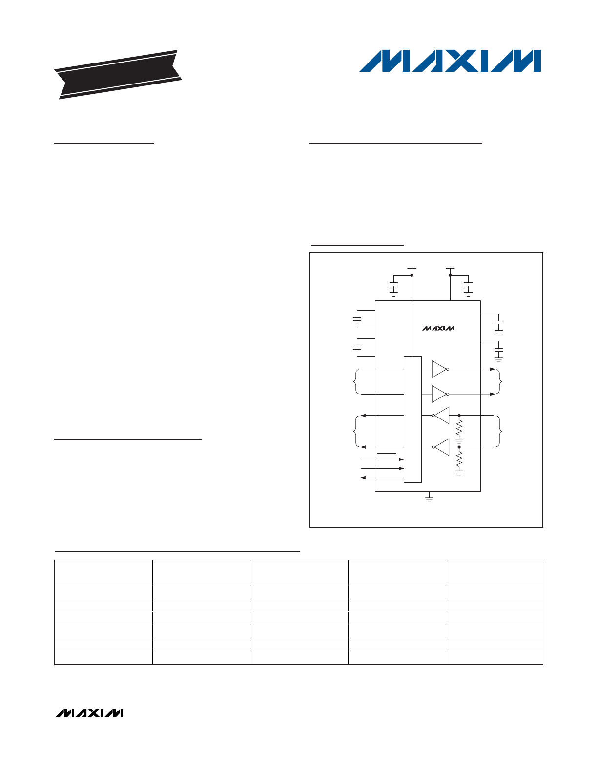
Functional Diagrams continued at end of data sheet.
+
Denotes a lead-free/RoHS-compliant package.
*
EP = Exposed pad.
Functional Diagrams
1.62V to V
CC
C
BYPASS1
V
L
MAX13234E
MAX13235E
TION
LOGIC-LEVEL TRANSLA
GND
TTL/CMOS
INPUTS
TTL/CMOS
OUTPUTS
C1
C1+
C1-
C2+
C2
C2-
T1IN
T2IN
R1OUT
R2OUT
FORCEOFF
FORCEON
READY
3.0V to 5.5V
V
CC
C
BYPASS2
V+
V-
T1OUT
T2OUT
R1IN
5kΩ
R2IN
5kΩ
C3
C4
RS-232
OUTPUTS
RS-232
INPUTS
Page 2
MAX13234E–MAX13237E
3Mbps RS-232 Transceivers with
Low-Voltage Interface
2 _______________________________________________________________________________________
ABSOLUTE MAXIMUM RATINGS
ELECTRICAL CHARACTERISTICS
(V
CC
= +3V to +5.5V, VL= +1.62V to VCC, TA= -40°C to +85°C, C1–C4 = 0.1µF, VCC= VL, tested at 3.3V ±10%. Typical values are
at TA= +25°C.) (Note 2)
Stresses beyond those listed under “Absolute Maximum Ratings” may cause permanent damage to the device. These are stress ratings only, and functional
operation of the device at these or any other conditions beyond those indicated in the operational sections of the specifications is not implied. Exposure to
absolute maximum rating conditions for extended periods may affect device reliability.
Note 1: Package thermal resistances were obtained using the method described in JEDEC specification JESD51-7, using a four-
layer board. For detailed information on package thermal considerations, refer to www.maxim-ic.com/thermal-tutorial
.
(All voltages referenced to GND.)
V
CC
...................................................................... -0.3V to +6.0V
V
L
......................................................................... -0.3V to +6.0V
V+ ........................................................................ -0.3V to +7.0V
V- ......................................................................... +0.3V to -7.0V
(V+) + |(V-)| ..................................................................... +13.0V
T_IN, FORCEOFF, FORCEON ..................... -0.3V to (V
L
+ 0.3V)
R_IN ................................................................................... ±25V
T_OUT.............................................................................. ±13.2V
R_OUT, READY ........................................... -0.3V to (V
L
+ 0.3V)
Short-Circuit Duration
T_OUT to GND ......................................................... Continuous
Continuous Power Dissipation (T
A
= +70°C)
16-Pin TQFN (derate 20.8mW/°C above +70°C) ..... 1666mW
20-Pn TSSOP (derate 10.9mW/°C above +70°C) ...... 879mW
20-Pin TQFN (derate 21.3mW/°C above +70°C) ..... 1702mW
Junction-to-Case Thermal Resistance (θ
JC
) (Note 1)
16-Pin TQFN ................................................................. 2°C/W
20-Pin TSSOP ............................................................. 20°C/W
20-Pin TQFN ................................................................. 2°C/W
Junction-to-Ambient Thermal Resistance (θ
JA
) (Note 1)
16-Pin TQFN ............................................................... 30°C/W
20-Pin TSSOP ............................................................. 73°C/W
20-Pin TQFN ............................................................... 29°C/W
Operating Temperature Range
MAX1323x Operating Temperature Range .... -40°C to +85°C
MAX1323x Operating Temperature Range .. -40°C to +105°C
Storage Temperature Range ........................... -65°C to +160°C
Lead Temperature (soldering, 10s) .................................+300
º
C
PARAMETER SYMBOL CONDITIONS MIN TYP MAX UNITS
Supply Voltage V
Logic Supply Voltage V
VCC Supply Current I
VCC Shutdown Current I
VL Supply Current I
VL Shutdown Current I
LOGIC INPUTS (T_IN, FORCEON, FORCEOFF, Referred to VL)
Input Threshold Low V
Input Threshold High V
Input Hysteresis 60 mV
Input Leakage Current ±0.01 ±1 µA
RECEIVER OUTPUTS (READY)
Output-Voltage Low V
Output-Voltage High V
CC
L
CC
CCSH
L
LSH
IL
IH
OL
OH
FORCEOFF = FORCEON = VL, no loads 0.3 1 mA
VL = 0V 1 10
AutoShutDown Plus, FORCEOFF = VL,
FORCEON = GND, all R_IN idle, all T_IN
idle.
FORCEOFF = GND 1 10 µA
VCC = +5.5V 1 10 µA
FORCEOFF = GND 1 10 µA
Tested at room temperature only 1/3 x V
Tested at room temperature only 2/3 x V
I
= 0.8mA 0.4 V
OUT
I
= -0.5mA VL - 0.6 VL - 0.1 V
OUT
3 5.5 V
1.62 V
110
L
CC
L
V
µA
V
V
Page 3
MAX13234E–MAX13237E
3Mbps RS-232 Transceivers with
Low-Voltage Interface
_______________________________________________________________________________________ 3
ELECTRICAL CHARACTERISTICS (continued)
(V
CC
= +3V to +5.5V, VL= +1.62V to VCC, TA= -40°C to +85°C, C1–C4 = 0.1µF, VCC= VL, tested at 3.3V ±10%. Typical values are
at TA= +25°C.) (Note 2)
RECEIVER INPUTS
Input-Voltage Range - 25 +25 V
Input Threshold Low V
Input Threshold High V
Input Hysteresis 0.5 V
Input Resistance 357kΩ
TRANSMITTER OUTPUTS
Output-Voltage Swing
Output Resistance
Output Short-Circuit Current -60 +60 mA
Output Leakage Current
AutoShutdown Plus (FORCEON = GND, FORCEOFF = VL)
Receiver Input Threshold Valid
Level
Receiver Input Threshold
Invalid Level
Receiver or Transmitter Edge-toTransmitters Enabled
Receiver or Transmitter Edge-toTransmitters Shutdown
TIMING CHARACTERISTICS (MAX13234E/MAX13236E)
Maximum Data Rate
Receiver Propagation Delay
Transmitter Skew
Receiver Skew
PARAMETER SYMBOL CONDITIONS MIN TYP MAX UNITS
IL
IH
t
WU
t
AUTOSHDNVL
t
,
RPHL
t
RPLH
|t
-
TPHL
t
|
TPLH
|t
-
RPHL
t
|
RPLH
TA = +25°C
TA = +25°C
All transmitter outputs loaded with 3kΩ to
GND
V
= V+ = V- = 0V, transmitter outputs =
CC
±2V
V
= 0V or +3V to +5.5V, V
CC
transmitters disabled
Positive threshold, Figure 1 2.7 V
Negative threshold, Figure 1 -2.7 V
Figure 1 -0.3 +0.3 V
VL = 5V, Figure 1 (Note 3) 100 µs
= 5V, Figure 1 (Note 3) 15 30 60 s
R
= 3kΩ, CL = 1000pF, one transmitter
L
switching
CL = 150pF, Figures 2, 3 0.15 µs
Figures 4, 5 (Note 4) 100 ns
Figures 2, 3 50 ns
VCC = +3.3V 0.6 1.2
= +5V 0.8 1.5
V
CC
VCC = +3.3V 1.5 2.4
= +5V 1.8 2.4
V
CC
±5 ±5.4 V
300 10M Ω
= ±12V,
OUT
-25 +25 µA
250 kbps
V
V
Page 4
MAX13234E–MAX13237E
3Mbps RS-232 Transceivers with
Low-Voltage Interface
4 _______________________________________________________________________________________
ELECTRICAL CHARACTERISTICS (continued)
(V
CC
= +3V to +5.5V, VL= +1.62V to VCC, TA= -40°C to +85°C, C1–C4 = 0.1µF, VCC= VL, tested at 3.3V ±10%. Typical values are
at TA= +25°C.) (Note 2)
Note 2: All devices are 100% production tested at TA= +85°C. All temperature limits are guaranteed by design.
Note 3: A transmitter/receiver edge is defined as a transition through the transmitter/receiver input-logic thresholds.
Note 4: Transmitter skew is measured at the transmitter zero cross points.
Transition-Region Slew Rate
TIMING CHARACTERISTICS (MAX13235E/MAX13237E)
Maximum Data Rate
Receiver Propagation Delay
Transmitter Skew
Receiver Skew
Transition-Region Slew Rate
ESD PROTECTION
PARAMETER SYMBOL CONDITIONS MIN TYP MAX UNITS
= +3.3V, TA = +25°C, RL = 3kΩ to 7kΩ,
V
CC
measured from +3V to -3V or -3V to +3V,
t
RPHL
t
RPLH
|t
TPHL
t
TPLH
|t
RPHL
t
RPLH
one transmitter switching, C
1000pF
RL = 3kΩ, CL = 250pF, one transmitter
switching
= 3kΩ, CL = 150pF, one transmitter
R
L
switching
,
CL = 150pF, Figures 2, 3 0.15 µs
–
Figures 4, 5 (Note 4) 25 ns
|
–
Figures 2, 3 50 ns
|
= +3.3V, TA = +25°C, RL = 3kΩ to 7kΩ,
V
CC
measured from T
to +3V, one transmitter switching, C
150pF to 1000pF
Human Body Model ±15
IEC 61000-4-2 Air Discharge ±15R_IN, T_OUT to GND
IEC 61000-4-2 Contact Discharge ±8
_OUT
= 150pF to
L
= +3V to -3V or -3V
6 30 V/µs
1
Mbps
3
=
L
24 150 V/µs
kV
Page 5
MAX13234E–MAX13237E
3Mbps RS-232 Transceivers with
Low-Voltage Interface
_______________________________________________________________________________________ 5
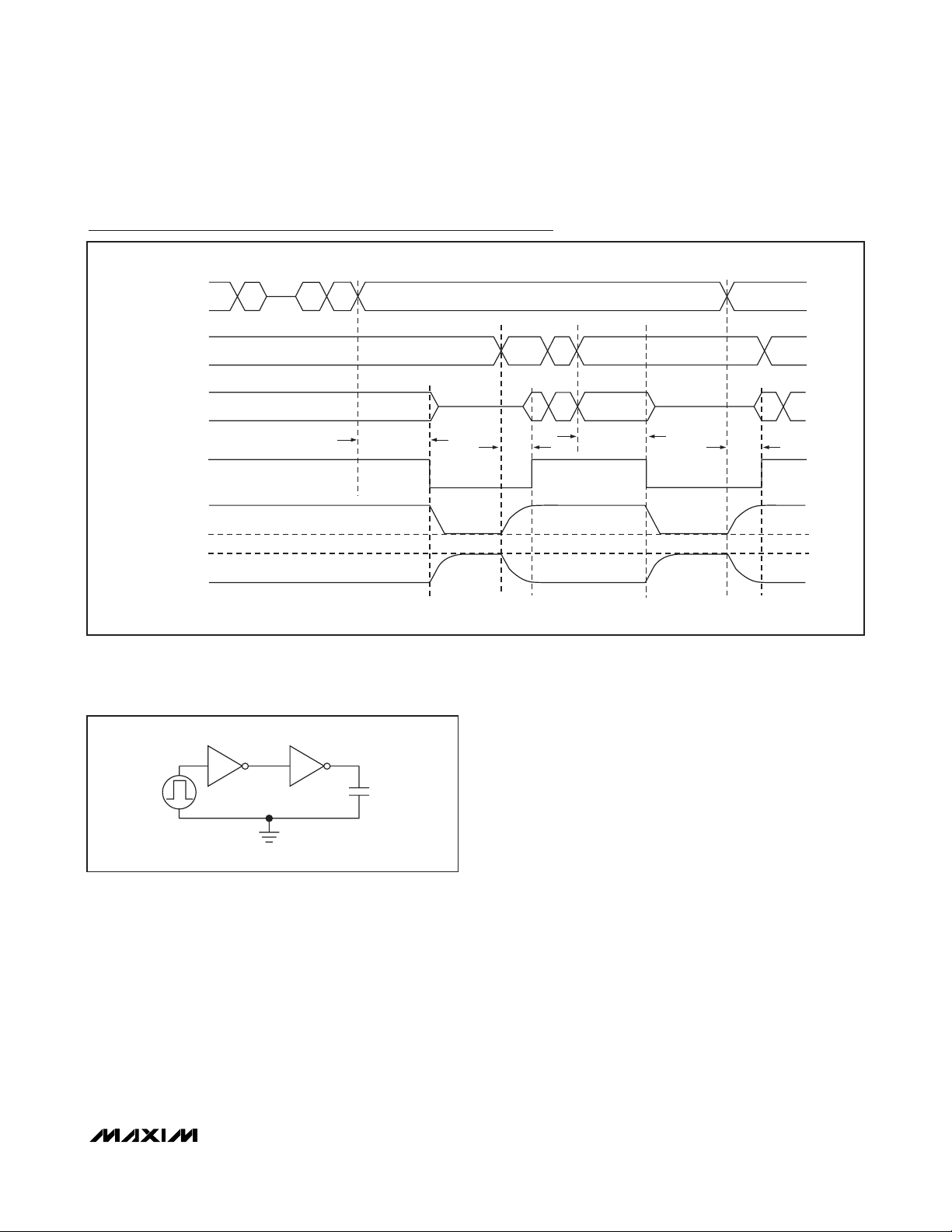
Test Circuits/Timing Diagram
Figure 1. AutoShutdown Plus, and READY Timing Diagram
Figure 2. Receiver Test Circuit
RECEIVER
INPUTS
TRANSMITTER
INPUTS
TRANSMITTER
OUTPUTS
t
AUTOSHDN
READY
V+
V-
V
CC
0
V+
V
CC
0
V-
t
t
WU
AUTOSHDN
t
WU
T_OUT R_OUTR_INT_IN
C
L
Page 6

MAX13234E–MAX13237E
3Mbps RS-232 Transceivers with
Low-Voltage Interface
6 _______________________________________________________________________________________
Test Circuits/Timing Diagram (continued)
Figure 5. Transmitter Propagation Delay
Figure 4. Transmitter Test Circuit
Figure 3. Receiver Propagation Delay
R_IN
V
OH
R_OUT
V
OL
1.3V
t
RPHL
/2
V
L
tR, tF ≤ 10ns
T_OUTT_IN
C
V
L
O
R
L
1.7V
t
RPLH
/2
V
L
V
T_IN
T_OUT
L
0
V
O
-V
O
VL/2 VL/2
t
TPHL
3V
0
-3V
t
F
SRF = 6/t
F
tR, tF ≤ 10ns
SRR = 6/t
t
TPLH
0
-3V
t
R
R
3V
Page 7

MAX13234E–MAX13237E
3Mbps RS-232 Transceivers with
Low-Voltage Interface
_______________________________________________________________________________________ 7
Typical Operating Characteristics
(VCC= VL= 3.3V, TA= +25°C, unless otherwise noted.)
TRANSMITTER OUTPUT VOLTAGE
vs. LOAD CAPACITANCE
MAX13234E toc01
LOAD CAPACITANCE (pF)
OUTPUT VOLTAGE (V)
500 20001000 1500
-4
-2
0
2
4
6
-6
0 2500
MAX13234E/MAX13236E
R
L
= 3k
Ω
T1 AT 250kbps
V+
V-
TRANSMITTER OUTPUT VOLTAGE
vs. LOAD CAPACITANCE
MAX13234E toc02
LOAD CAPACITANCE (pF)
OUTPUT VOLTAGE (V)
100 250150 200
-4
-2
0
2
4
6
-6
50 300
MAX13235E/MAX13237E
R
L
= 3k
Ω
T1 AT 3Mbps
V+
V-
SLEW RATE vs. LOAD CAPACITANCE
MAX13234E toc03
LOAD CAPACITANCE (pF)
SLEW RATE (V/µs)
500 20001000 1500
6
7
8
10
5
9
11
12
4
0 2500
MAX13234E/MAX13236E
R
L
= 3kΩ
SR+
SR-
SLEW RATE vs. LOAD CAPACITANCE
MAX13234E toc04
LOAD CAPACITANCE (pF)
SLEW RATE (V/µs)
100 250150 200
50
55
60
70
45
65
75
40
50 300
MAX13235E/MAX13237E
R
L
= 3k
Ω
SR+
SR-
VCC SUPPLY CURRENT
vs. LOAD CAPACITANCE
MAX13234E toc05
LOAD CAPACITANCE (pF)
SUPPLY CURRENT (mA)
500 20001000 1500
10
15
25
5
20
30
0
0 2500
MAX13234ERL = 3k
Ω
T1 AT 250kbps
T2 AT 15.6kbps
VCC SUPPLY CURRENT
vs. LOAD CAPACITANCE
MAX13234E toc06
LOAD CAPACITANCE (pF)
SUPPLY CURRENT (mA)
100 250150 200
15
20
30
35
10
25
40
5
50 300
MAX13235ERL = 3k
Ω
T1 AT 3Mbps
T2 AT 187.5kbps
TRANSMITTER SKEW
vs. LOAD CAPACITANCE
MAX13234E toc07
LOAD CAPACITANCE (pF)
TRANSMITTER SKEW (ns)
500 20001000 1500
30
50
90
110
130
10
70
150
-10
0 2500
MAX13234E/MAX13236E
R
L
= 3k
Ω
1 TRANSMITTER
OPERATING AT 250kbps
TRANSMITTER SKEW
vs. LOAD CAPACITANCE
MAX13234E toc08
LOAD CAPACITANCE (pF)
TRANSMITTER SKEW (ns)
150 200100
3
4
6
7
8
2
1
5
9
0
50 250
MAX13235E/MAX13237E
R
L
= 3k
Ω
1 TRANSMITTER
OPERATING AT 3Mbps
READY TURN-ON TIME
vs. TEMPERATURE
MAX13234E toc09
TEMPERATURE (°C)
READY TURN-ON TIME (µs)
-15 6010 35
50
60
70
80
90
100
40
-40 85
Page 8

MAX13234E–MAX13237E
3Mbps RS-232 Transceivers with
Low-Voltage Interface
8 _______________________________________________________________________________________
Typical Operating Characteristics (continued)
(VCC= VL= 3.3V, TA= +25°C, unless otherwise noted.)
READY TURN-OFF TIME
2.0
1.8
1.6
1.4
1.2
1.0
0.8
0.6
READY TURN-OFF TIME (µs)
0.4
0.2
0
-15 6010 35
-40 85
TEMPERATURE (°C)
MAX13234E toc10
TRANSMITTER OUTPUT VOLTAGE
vs. SUPPLY VOLTAGE
8
vs. TEMPERATURE
6
4
2
MAX13235E/MAX13237E
= 3kΩ, CL = 150pF
R
L
0
1 TRANSMITTER
OPERATING AT 1Mbps
-2
OUTPUT VOLTAGE (V)
-4
-6
-8
3.5 4.54.0 5.0
3.0 5.5
V+
V-
SUPPLY COLTAGE (V)
SUPPLY CURRENT vs. DATA RATE
35
MAX13235E
1 TRANSMITTER
30
OPERATING
= 3kΩ, CL = 150pF
R
L
25
20
15
SUPPLY CURRENT (mA)
10
5
0
0.001 10
0.1 10.01
DATA RATE (kbps)
MAX13234E toc13
-2
OUTPUT VOLTAGE (V)
-4
-6
-8
8
6
4
2
0
08
TRANSMITTER OUTPUT VOLTAGE
1 TRANSMITTER
OPERATING, DC
2.5
2.3
2.1
MAX13234E toc11
1.9
1.7
1.5
1.3
1.1
LOGIC-INPUT THRESHOLD (V)
0.9
0.7
0.5
1.5 5.5
vs. LOAD CURRENT
V+
V-
264
LOAD CURRENT (mA)
LOGIC-INPUT THRESHOLD vs. V
VCC = 5.5V
V
IH
V
IL
3.5 4.52.5
VL (V)
MAX13234E toc14
L
MAX13234E toc12
Page 9

MAX13234E–MAX13237E
3Mbps RS-232 Transceivers with
Low-Voltage Interface
_______________________________________________________________________________________ 9
Pin Descriptions
PIN
MAX13234E/
MAX13235E
TSSOP TQFN-EP TQFN-EP
1 19 14 READY
2 1 16 C1+
3 20 15 V+ +5.5V Generated by the Charge Pump
4 2 1 C1-
5 3 2 C2+ Positive Terminal of the Inverting Charge-Pump Capacitor
6 4 3 C2- Negative Terminal of the Inverting Charge-Pump Capacitor
7 5 4 V- -5.5V Generated by the Charge Pump
8 6 — T2OUT RS-232 Transmitter Output 2
— — 5 RIN RS-232 Receiver Input
9 7 — R2IN RS-232 Receiver Input 2
— — 6 ROUT CMOS Receiver Output. VL referred logic.
10 8 — R2OUT CMOS Receiver Output 2. VL referred logic.
11 9 7 V
— — 8 TIN CMOS Transmitter Input. VL referred logic.
12 10 — T2IN CMOS Transmitter Input 2. VL referred logic.
13 11 — T1IN CMOS Transmitter Input 1. VL referred logic.
14 12 9 FORCEON
15 13 — R1OUT CMOS Receiver Output 1. VL referred logic.
— — 10 TOUT RS-232 Transmitter Output
16 14 — R1IN RS-232 Receiver Input 1
17 15 — T1OUT RS-232 Transmitter Output 1
18 16 11 GND Ground
19 17 12 V
20 18 13 FORCEOFF
— — — EP Exposed Pad. Connect EP to GND or leave unconnected.
MAX13236E/
MAX13237E
NAME FUNCTION
Ready to Transmit Output, Active-High. READY is enabled
high when V- goes below -4V and the device is ready to
transmit.
Positive Terminal of the Voltage Doubler Charge-Pump
Capacitor
Negative Terminal of the Voltage Doubler Charge-Pump
Capacitor
L
CC
Logic-Level Supply. All CMOS inputs and outputs are related
to this supply.
FORCEON Input, Active-High. V
FORCEON high to override automatic circuitry keeping
transmitters on (FORCEOFF must be high).
See Table 1.
+3V to +5.5V Supply Voltage
FORCEOFF Input, Active-Low. V
FORCEOFF low to shut down transmitters and on-board
charge pumps. All receiver and transmitter outputs are tristated. This overrides all automatic circuitry and FORCEON
(Table 1).
referenced logic. Drive
L
referenced logic. Drive
L
Page 10

MAX13234E–MAX13237E
3Mbps RS-232 Transceivers with
Low-Voltage Interface
10 ______________________________________________________________________________________
Detailed Description
VL Logic Supply Input
The MAX13234E–MAX13237E feature a separate logic
supply input (V
L
) that sets the receiver’s output level
(V
OH
), and sets the transmitter’s input thresholds (VIL,
V
IH
). This feature allows flexibility in interfacing to
UARTs or communication controllers that have different
logic levels. Connect this input to the host logic supply
(1.62V ≤ VL≤ VCC).
Dual Charge-Pump Voltage Converter
The internal power supply consists of a regulated dual
charge pump that provides output voltages of +5.5V
and -5.5V (inverting charge pump), over the +3.0V to
+5.5V range. The charge pump operates in discontinuous mode: if the output voltages are less than +5.5V,
the charge pump is enabled; if the output voltages
exceed +5.5V, the charge-pump is disabled. The
charge pumps require flying capacitors (C1, C2) and
reservoir capacitors (C3, C4) to generate the V+ and Vsupplies. The READY output is low when the charge
pumps are disabled in shutdown mode. The READY
signal asserts high when V- goes below -4V.
RS-232 Transmitters
The transmitters are inverting level translators that convert CMOS-logic levels to ±5.0V EIA/TIA-232 levels.
The MAX13234E/MAX13236E guarantee a 250kbps
data rate with worst-case loads of 3kΩ in parallel with
1000pF. The MAX13235E/MAX13237E guarantee a
1Mbps data rate with worst-case loads of 3kΩ in parallel with 250pF, and a 3Mbps data rate with worst-case
loads of 3kΩ in parallel with 150pF. Transmitters can be
paralleled to drive multiple receivers. When FORCEOFF
is driven to ground or when the AutoShutdown Plus circuitry senses that all receiver and transmitter inputs are
inactive for more than 30s, the transmitters are disabled
and the outputs go into a high-impedance state. When
powered off or shut down, the outputs can be driven to
±12V. The transmitter inputs do not have pullup resistors. Connect unused inputs to GND or VL.
RS-232 Receivers
The receivers convert RS-232 signals to CMOS-logic
output levels. The MAX13234E–MAX13237E have
inverting outputs that are active when in shutdown
(FORCEOFF = GND) (Table 1).
AutoShutdown Plus Mode
Drive FORCEOFF high and FORCEON low to invoke
AutoShutdown Plus mode. When these devices do not
sense a valid signal transition on any receiver and
transmitter input for 30s, the onboard charge pumps
are shut down, reducing supply current to 1µA. This
occurs if the RS-232 cable is disconnected or
if the devices driving the transmitter and receiver
inputs are inactive for more than 30s. The
MAX13234E–MAX13237E turn on again when a valid
transition is applied to any RS-232 receiver or transmitter input. As a result, the system saves power without
requiring any control.
Figure 6 and Table 1 summarize the MAX13234E–
MAX13237E operating modes. The FORCEON and
FORCEOFF inputs override AutoShutdown Plus circuitry. When neither control is asserted, the IC selects
between these states automatically based on the last
receiver or transmitter input edge received.
Hardware-Controlled Shutdown
Drive FORCEOFF low to place the MAX13234E–
MAX13237E into shutdown mode.
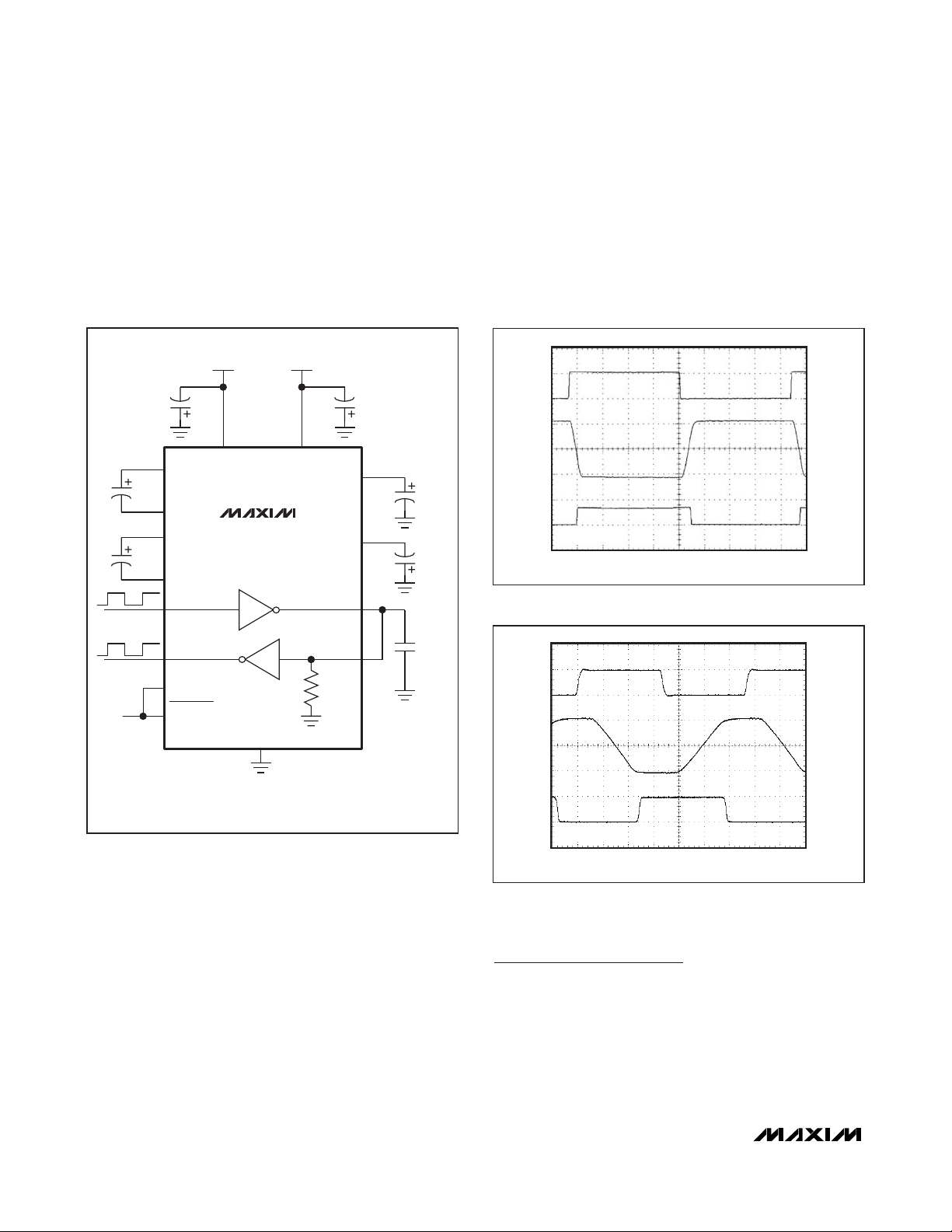
Figure 7. AutoShutdown Plus Initial Turn-On to Wake Up a
Mouse or Another System
POWER-
MANAGEMENT
UNIT
MASTER SHDN LINE
FORCEOFF
0.1µF1MΩ
FORCEON
MAX13234E
MAX13235E
MAX13236E
MAX13237E
Page 11

MAX13234E–MAX13237E
3Mbps RS-232 Transceivers with
Low-Voltage Interface
______________________________________________________________________________________ 11
Table 1. Transceiver Mode Control
X = Don’t Care.
Figure 6. AutoShutdown Plus and Shutdown Logic
T_IN
R_IN
EDGE
DETECT
EDGE
DETECT
FORCEON
FORCEOFF
S
30s
TIMER
R
FORCEOFF
FORCEON
AUTOSHDN
* POWERDOWN IS ONLY AN INTERNAL SIGNAL.
IT CONTROLS THE OPERATIONAL STATUS OF
THE TRANSMITTERS AND THE POWER SUPPLIES.
POWERDOWN*
FORCEOFF FORCEON
0 X X High-Impedance Active Shutdown (Forced Off)
1 1 X Active Active Normal Operation (Forced On)
1 0 Yes Active Active Normal Operation in AutoShutdown Plus
1 0 No High-Impedance Active Shutdown in AutoShutdown Plus
R_IN or T_IN
EDGE WITHIN 30s
T_OUT R_OUT TRANSCEIVER STATUS
Page 12

MAX13234E–MAX13237E
3Mbps RS-232 Transceivers with
Low-Voltage Interface
12 ______________________________________________________________________________________
Figure 8a. Human Body ESD Test Model
Figure 8b. Human Body Current Waveform
Figure 9a. IEC61000-4-2 ESD Test Model
Figure 9b. IEC61000-4-2 ESD Generator Current Waveform
±15kV ESD Protection
ESD-protection structures are incorporated on all pins
to protect against electrostatic discharges encountered
during handling and assembly. The driver outputs and
receiver inputs of the MAX13234E–MAX13237E have
extra protection against static electricity. Maxim’s engineers have developed state-of-the-art structures to protect these pins against ESD of ±15kV without damage.
The ESD structures withstand high ESD in all states:
normal operation, shutdown, and powered down. After
an ESD event, Maxim’s E versions keep working without
latchup. ESD protection can be tested in various ways;
the transmitter outputs and receiver inputs of this product family are characterized for protection to the following limits:
1) ±15V Using the Human Body Model
2) ±15kV Using IEC 61000-4-2 Air-Gap Method
3) ±8kV Using IEC 61000-4-2 Contact-Discharge
Method
R
D
1500Ω
DISCHARGE
RESISTANCE
STORAGE
CAPACITOR
DEVICE
UNDER
TEST
HIGH-
VOLTAGE
DC
SOURCE
R
C
1MΩ
CHARGE-CURRENT
LIMIT RESISTOR
C
100pF
s
R
D
330Ω
DISCHARGE
RESISTANCE
STORAGE
CAPACITOR
DEVICE
UNDER
TEST
HIGH-
VOLTAGE
DC
SOURCE
R
C
50MΩ to 100MΩ
CHARGE-CURRENT
LIMIT RESISTOR
C
150pF
s
AMPERES
IP 100%
90%
36.8%
10%
0
0
t
RL
I
r
TIME
t
DL
CURRENT WAVEFORM
PEAK-TO-PEAK RINGING
(NOT DRAWN TO SCALE)
I
100%
90%
PEAK
I
10%
tr = 0.7ns to 1ns
30ns
60ns
t
Page 13

ESD Test Conditions
ESD performance depends on a variety of conditions.
Contact Maxim for a reliability report that documents
test setup, test methodology, and test results.
Human Body Model
Figure 8a shows the Human Body Model and Figure 8b
shows the current waveform it generates when discharged into a low impedance. This model consists of
a 100pF capacitor charged to the ESD voltage of interest, which is then discharged into the test device
through a 1.5kΩ resistor.
IEC 61000-4-2
The IEC 61000-4-2 standard covers ESD testing and
performance of finished equipment; it does not specifically refer to integrated circuits. The MAX13234E–
MAX13237E helps design equipment that meets Level
4 (the highest level) of IEC 61000-4-2, without the need
for additional ESD-protection components. The major
difference between tests done using the Human Body
Model and IEC 61000-4-2 is higher peak current in IEC
61000-4-2, because series resistance is lower in the
IEC 61000-4-2 model. Hence, the ESD withstand voltage measured to IEC 61000-4-2 is generally lower than
that measured using the Human Body Model. Figure 9a
shows the IEC 61000-4-2 model and Figure 9b shows
the current waveform for the 8kV, IEC 61000-4-2, Level
4, ESD Contact-Discharge Method.
The Air-Gap Method involves approaching the device
with a charged probe. The Contact-Discharge Method
connects the probe to the device before the probe is
energized.
Applications Information
Capacitor Selection
The capacitor type used for C1–C4 is not critical for
proper operation; polarized or non-polarized capacitors
can be used. The charge pump requires 0.1µF capacitors for VCC= +3.3V operation. For other supply voltages, see Table 2 for required capacitor values. Do not
use values smaller than those listed in Table 2.
Increasing the capacitor values (e.g., by a factor of 2)
reduces ripple on the transmitter outputs and slightly
reduces power consumption. C2, C3, and C4 can be
increased without changing C1’s value. However, do
not increase C1 without also increasing the values
of C2, C3, C4, C
BYPASS1
, and C
BYPASS2
to maintain
the proper ratios (C1 to the other capacitors). When
using the minimum required capacitor values, make
sure the capacitor value does not degrade excessively
with temperature. If in doubt, use capacitors with a
larger nominal value. The capacitor’s equivalent series
resistance (ESR), usually rises at low temperatures
influencing the amount of ripple on V+ and V-.
Power-Supply Decoupling
In most circumstances, a 0.1µF VCCbypass capacitor
and a 1µF VLbypass capacitor are adequate. In applications that are sensitive to power-supply noise, use
capacitors of the same value as charge-pump capacitor C1. Connect bypass capacitors as close to the IC
as possible.
Transmitter Outputs when Exiting
Shutdown
Figure 10 shows two transmitter outputs when exiting
shutdown mode. As they become active, the two transmitter outputs are shown going to opposite RS-232 levels (one transmitter input is high, the other is low). Each
transmitter is loaded with 3kΩ in parallel with 1000pF.
The transmitter outputs display no ringing or undesirable transients as they come out of shutdown. Note that
the transmitters are enabled only when the magnitude
of V- exceeds approximately -3V.
MAX13234E–MAX13237E
3Mbps RS-232 Transceivers with
Low-Voltage Interface
______________________________________________________________________________________ 13
Table 2. Required Minimum Capacitance
Values
Figure 10. Transmitter Outputs when Exiting Shutdown or
Powering Up
V
CC
(V)
3.0 to 3.6 0.22 0.22 0.22
3.15 to 3.6 0.1 0.1 0.1
4.5 to 5.5 0.047 1 0.33
3.0 to 5.5 0.22 1 1
C1, C
BYPASS2
(µF)
C
BYPASS1
(µF)
C2, C3, C4
(µF)
5V/div
0
2V/div
0
VCC = 3.3V
5V/div
C1–C4 = 0.1µF
0
5µs/div
FORCEON = FORCEOFF
T1OUT
T2OUT
READY
Page 14
MAX13234E–MAX13237E
3Mbps RS-232 Transceivers with
Low-Voltage Interface
14 ______________________________________________________________________________________
Figure 12. Loopback Test Results at 120kbps
Figure 13. Loopback Test Results at 3Mbps
Figure 11. Loopback Test Circuit
Chip Information
PROCESS: BiCMOS
High Data Rates
The MAX13234E–MAX13237E maintain the RS-232 ±5V
minimum transmitter output voltage even at high data
rates. Figure 11 shows a transmitter loopback test circuit. Figure 12 shows a loopback test result at
120kbps, and Figure 13 shows the same test at 3Mbps.
In Figure 12, all transmitters were driven simultaneously
at 120kbps into RS-232 loads in parallel with 1000pF.
In Figure 13, a single transmitter was driven at 3Mbps,
and all transmitters were loaded with an RS-232 receiver in parallel with 150pF.
1.62V to V
CC
C
BYPASS1
V
C1+
C1
C1-
C2+
C2
C2-
T_IN
L
MAX13236E
MAX13237E
V
CC
C
BYPASS2
V
CC
V+
C3*
V-
C4
T_OUT
R_OUT
FORCEON
V
CC
FORCEOFF
GND
R_IN
5kΩ
1000pF
T1IN
T1OUT
R1OUT
VCC = 3.3V
2µs/div
T1IN
T1OUT
3V/div
5V/div
5V/div
3.3V/div
5V/div
*C3 CAN BE RETURNED TO V
OR GND.
CC
R1OUT
VCC = 3.3V
100ns/div
3.3V/div
Page 15
MAX13234E–MAX13237E
3Mbps RS-232 Transceivers with
Low-Voltage Interface
______________________________________________________________________________________ 15
Pin Configurations
Functional Diagrams (continued)
READY
C1+
C1-
C2+
C2-
T2OUT
R2IN
R2OUT
TOP VIEWTOP VIEW
+
1
2
V+
3
4
MAX13234E
MAX13235E
6
V-
7
8
9
TSSOP
20
19
18
17
165
15
14
13
12
1110
FORCEOFF
V
CC
GND
T1OUT
R1IN
R1OUT
FORCEON
T1IN
T2IN
V
L
R1IN
T1OUTC1+
15
GND
16
V
17
FORCEOFF
READY
CC
18
19
V+
MAX13234E
MAX13235E
+
2143134125
1
C1-
TQFN
*EXPOSED PAD. CONNECT EP TO GND.
R1OUT
C2+
T1IN
FORCEON
11
*EP
V-
C2-
T2IN
10
V
9
L
R2OUT
8
R2IN
7
T2OUT
620
1.62V to V
CC
3.0V to 5.5V
TOP VIEW
CC
GND
V
FORCEOFF
READY
C1+
13
14
MAX13236E
15
16
MAX13237E
+
1122113104
C1-
C2+
V+
TQFN
*EXPOSED PAD. CONNECT EP TO GND.
TOUT
*EP
C2-
FORCEON
9
V-
TIN
8
V
7
L
ROUT
6
RIN
5
5kΩ
T_OUT
R_IN
C
BYPASS2
V+
V-
C3
C4
RS-232
OUTPUT
RS-232
INPUT
C1
C2
TTL/CMOS
INPUT
TTL/CMOS
OUTPUT
C
BYPASS1
C1+
C1-
C2+
C2-
T_IN
R_OUT
FORCEOFF
FORCEON
READY
V
L
LOGIC-LEVEL TRANSLATION
MAX13236E
MAX13237E
GND
V
CC
Page 16

MAX13234E–MAX13237E
3Mbps RS-232 Transceivers with
Low-Voltage Interface
Maxim cannot assume responsibility for use of any circuitry other than circuitry entirely embodied in a Maxim product. No circuit patent licenses are
implied. Maxim reserves the right to change the circuitry and specifications without notice at any time.
16
____________________Maxim Integrated Products, 120 San Gabriel Drive, Sunnyvale, CA 94086 408-737-7600
© 2008 Maxim Integrated Products is a registered trademark of Maxim Integrated Products, Inc.
PACKAGE TYPE PACKAGE CODE DOCUMENT NO.
20 TSSOP U20-2
21-0066
20 TQFN-EP* T2055-5
21-0140
16 TQFN-EP* T1655-2
21-0140
Package Information
For the latest package outline information and land patterns, go to www.maxim-ic.com/packages.
*
EP = Exposed Pad.
 Loading...