

Page 1
General Description
The MAX13181E–MAX13184E are full-duplex and selectable half-/full-duplex RS-485 transceivers in a tiny 2mm x
2mm µDFN package. These devices are designed for
space-constrained applications by including extended
ESD protection to ±15kV per Human Body Model (HBM)
and integrating pullup/pulldown resistors on the DE, RE
and H/F inputs to reduce external components. The
MAX13182E/MAX13184E feature a low-current shutdown
mode for power-sensitive applications.
These devices have a 1/8 unit-load input receiver
that allows up to 256 transceivers on the bus. The
MAX13181E/MAX13182E feature reduced slew-rate
drivers to minimize EMI and reflections that are caused
by improperly terminated cables. The slew-rate limited
MAX13181E/MAX13182E allow error-free data transmission up to 250kbps. The MAX13183E/MAX13184E feature
full-speed drivers, allowing data rates of up to 16Mbps.
The MAX13182E/MAX13184E are configured for fullduplex operation, while the MAX13181E/MAX13183E
feature pin-selectable half- or full-duplex operation. All
driver outputs and receiver inputs include extended
ESD protection.
The MAX13181E–MAX13184E are available in a tiny 10pin, 2mm x 2mm µDFN. The MAX13183E/MAX13184E are
also available in industry-standard 14-pin SO packages.
The devices operate over the extended -40°C to +85°C
temperature range.
Applications
Features
♦ Available in Tiny, 10-Pin, 2mm x 2mm, µDFN and
14-Pin SO Packages
♦ +5.0V Operation
♦ Extended ESD Protection
±15kV Human Body Model
±12kV IEC 61000-4-2 Air-Gap Disharge
±6kV IEC 61000-4-2 Contact Disharge
♦ Slew-Rate Limiting Facilitates Error-Free Data
Transmission (MAX13181E/MAX13182E)
♦ 2.5µA (typ) Low-Current Shutdown Mode
♦ 1/8-Unit Load Allows Up to 256 Transceivers on
the Bus
MAX13181E–MAX13184E
+5.0V, ±15kV ESD-Protected, Half-Duplex/
Full-Duplex, RS-485 Transceiver in µDFN
________________________________________________________________
Maxim Integrated Products
1
19-0879; Rev 0; 7/07
For pricing delivery, and ordering information please contact Maxim Direct at 1-888-629-4642,
or visit Maxim’s website at www.maxim-ic.com.
Ordering Information
+
Denotes a lead-free package.
Industrial Control
Motor Drive Control
Telecom
Security System
Instrumentation
Selector Guide
Ordering Information continued at end of data sheet.
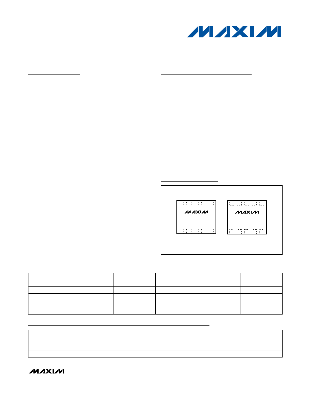
Pin Configurations
MAX13182E
MAX13184E
1019283746
5
V
CC
RO RE DE DI
A
TOP VIEW
BZ
µDFN
+
+
Y GND
MAX13181E
MAX13183E
1019283746
5
V
CC
RO H/F DE DI
ABZ
µDFN
Y GND
Pin Configurations continued at end of data sheet.
PART
MAX13181E Selectable 250 kbps Yes No No
MAX13182E Full 250 kbps Yes Yes Yes
MAX13183E Selectable 16 Mbps No No No
MAX13184E Full 16 Mbps No Yes Yes
HALF/FULL
DUPLEX
MAXIMUM DATA
RATE
SLEW-RATE
LIMITED
LOW-POWER
SHUTDOWN
RECEIVER
ENABLE
PART TEMP RANGE PIN-PACKAGE TOP MARK PKG CODE
MAX13181EELB+ -40°C to +85°C 10 µDFN ABC L1022-1
MAX13182EELB+ -40°C to +85°C 10 µDFN ABD L1022-1
MAX13182EESD+ -40°C to +85°C 14 SO — S14-1
Page 2
MAX13181E–MAX13184E
+5.0V, ±15kV ESD-Protected, Half-Duplex/
Full-Duplex, RS-485 Transceiver in µDFN
2 _______________________________________________________________________________________
ABSOLUTE MAXIMUM RATINGS
DC ELECTRICAL CHARACTERISTICS
(VCC= +5V ±10%, TA=T
MIN
to T
MAX
, unless otherwise noted. Typical values are at VCC= +5V and TA= +25°C.) (Note 1)
Stresses beyond those listed under “Absolute Maximum Ratings” may cause permanent damage to the device. These are stress ratings only, and functional
operation of the device at these or any other conditions beyond those indicated in the operational sections of the specifications is not implied. Exposure to
absolute maximum rating conditions for extended periods may affect device reliability.
(All voltages referenced to GND.)
Supply Voltage (V
CC
) ...............................................-0.3V to +6V
Control Voltage (RE, DE, DI, H/F).............................-0.3V to +6V
Driver Output Voltage (A, B, Y, Z) ..........................-8V to +12.5V
Receiver Input Voltage (A, B).................................-8V to +12.5V
Receiver Input Voltage Full-Duplex (A, B)..............-8V to +12.5V
Receiver Output Voltage (RO)................... -0.3V to (V
CC
+ 0.3V)
Short-Circuit Duration (A, B, Y, Z) to GND .................Continuous
Continuous Power Dissipation (T
A
= +70°C)
10-Pin µDFN (derate 5mW/°C above +70°C ) .............403mW
14-Pin SO (derate 8.3mW/°C above +70°C )...............667mW
Operating Temperature Range ...........................-40°C to +85°C
Storage Temperature Range .............................-65°C to +150°C
Junction Temperature......................................................+150°C
Lead Temperature (soldering, 10s) .................................+300°C
PARAMETER SYMBOL CONDITIONS MIN TYP MAX UNITS
DRIVER
Differential Driver Output V
Change in Magnitude of Differential
Output Voltage
Driver Common-Mode Output Voltage V
Change in Magnitude
of Common-Mode Voltage
Input-High Voltage V
Input-Low Voltage V
Input Hysteresis V
Internal Pullup Resistance R
Internal Pulldown Resistance R
Output Leakage (Y and Z)
Full-Duplex
Driver Short-Circuit Output Current
Threshold (Note 3)
Driver Short-Circuit Foldback Output
Current (Note 3)
Thermal-Shutdown Threshold T
Thermal-Shutdown Hysteresis T
Input Current (A and B) I
RL = 100Ω (RS422), Figure 1 2 V
RL = 54Ω (RS485), Figure 1 1.5 V
OD
No load V
ΔV
ΔV
IN_UP
IN_DWN
I
OSD
I
OSDF
A, B
RL = 100Ω or 54Ω, Figure 1, (Note 2) 0.2 V
OD
RL = 100Ω or 54Ω, Figure 1 V
OC
RL = 100Ω or 54Ω, Figure 1, (Note 2) 0.2 V
OC
DE, DI, RE, H/F 2V
IH
DE, DI, RE, H/F 0.8 V
IL
DE, DI, RE, H/F 100 mV
HYS
Internal pullup RE 125 400 kΩ
Internal pulldown DE, H/F 125 400 kΩ
DE = GND, VCC = GND or
I
O
5.5V
0 ≤ V
-7 ≤ V
(VCC - 1V) ≤ V
-7V ≤ V
0 ≤ V
TS
15 °C
TSH
D E = GN D , V
5.5V
≤ 12V 40 250
OUT
≤ V
OUT
CC
≤ 12V 20
OUT
≤ 1V -20
OUT
≤ 12V 140 °C
OUT
= GN D or
C C
VIN = +12V 125
= -7V -100
V
IN
VIN = +12V 125
V
= -7V -100
IN
CC
CC
CC
/ 2 3 V
CC
-250 -40
V
V
µA
mA
mA
µA
Page 3
MAX13181E–MAX13184E
+5.0V, ±15kV ESD-Protected, Half-Duplex/
Full-Duplex, RS-485 Transceiver in µDFN
_______________________________________________________________________________________ 3
DC ELECTRICAL CHARACTERISTICS (continued)
(VCC= +5V ±10%, TA=T
MIN
to T
MAX
, unless otherwise noted. Typical values are at VCC= +5V and TA= +25°C.) (Note 1)
DRIVER SWITCHING CHARACTERISTICS—MAX13181E/MAX13182E (SLEW-RATE LIMITED
TO 250kbps)
(VCC= +5V ±10%, TA=T
MIN
to T
MAX
, unless otherwise noted. Typical values are at VCC= +5V and TA= +25°C.) (Note 1)
)
)
PARAMETER SYMBOL CONDITIONS MIN TYP MAX UNITS
RECEIVER
Receiver Differential Threshold
Voltage
Receiver Input Hysteresis V
RO Output-High Voltage V
RO Output-Low Voltage V
Tri-State Output Current at Receiver I
Receiver-Input Resistance R
Receiver-Output Short-Circuit Current I
SUPPLY CURRENT
Supply Current I
Shutdown Current
(MAX13182E/MAX13184E Only)
ESD PROTECTION
ESD Protection for Y, Z, A and B
V
OZR
OSR
I
SHDN
-7V ≤ VCM ≤ +12V, Figure 2 -200 0 +200 mV
TH
VA + VB = 0, Figure 2 25 mV
TH
OHIO
OL
IN
CC
= -1mA, Figure 2
IO = 1mA, Figure 2 0.4 V
0 ≤ VO ≤ VCC, Figure 2 -1 +1 µA
-7V ≤ VCM ≤ +12V, Figure 2 96 kΩ
0 ≤ VRO ≤ VCC, Figure 2 -80 +80 mA
No load, RE = 0, DE = V
No load, RE = VCC, DE = V
No load, RE = 0V, DE = 0 or leave
unconnected
RE = V
DE = GND or leave unconnected
Human Body Model ±15
IEC 61000-4-2 Contact Discharge ±6
IEC 61000-4-2 Air-Gap Discharge ±12
or leave unconnected,
CC
CC
CC
V
-
CC
0.6
23
23
23
2.5 10 µA
V
mA
kV
Driver Propagation Delay
Driver Differential Output Rise or
Fall Time
Differential Driver Output Skew
(t
DPLH
Maximum Data Rate 250 kbps
Driver Enable to Output High t
Driver Enable to Output Low t
Driver Disable Time from Low t
Driver Disable Time from High t
D r i ver E nab l e fr om S hutd ow n to Outp ut H i g ht
D r i ver E nab l e fr om S hutd ow n to Outp ut Low t
Time to Shutdown t
PARAMETER SYMBOL CONDITIONS MIN TYP MAX UNITS
- t
)
DPHL
t
DPLH
t
DPHL
t
, t
DR
t
DSKEW
DZH
DZL
DLZ
DHZ
DZH(SHDN
DZL(SHDN
SHDN
CL = 50pF, RL = 54Ω, Figure 3 200 1000
CL = 50pF, RL = 54Ω, Figure 3 200 1000
CL = 50pF, RL = 54Ω, Figure 3 400 1200 ns
DF
CL = 50pF, RL = 54Ω, Figure 3 140 ns
Figure 4a 2500 ns
Figure 4b 2500 ns
Figure 4b 100 ns
Figure 4a 100 ns
(MAX13182E) Figure 4a 5500 ns
(MAX13182E) Figure 4b 5500 ns
(MAX13182E) 50 200 600 ns
ns
Page 4
MAX13181E–MAX13184E
+5.0V, ±15kV ESD-Protected, Half-Duplex/
Full-Duplex, RS-485 Transceiver in µDFN
4 _______________________________________________________________________________________
DRIVER SWITCHING CHARACTERISTICS—MAX13183E/MAX13184E (MAXIMUM DATA
RATE OF 16Mbps)
(VCC= +5V ±10%, TA=T
MIN
to T
MAX
, unless otherwise noted. Typical values are at VCC= +5V and TA= +25°C.) (Note 1)
(
)
(
)
RECEIVER SWITCHING CHARACTERISTICS
(VCC= +5V ±10%, TA=T
MIN
to T
MAX
, unless otherwise noted. Typical values are at VCC= +5V and TA= +25°C.) (Note 1)
(
)
(
)
Note 1: All currents into the device are positive. All currents out of the device are negative. All voltages are referred to device ground,
unless otherwise noted. µDFN devices are production tested at +25°C. Overtemperature limits are guaranteed by design.
Note 2: ΔV
OD
and ΔVOCare the changes in VODand VOC, respectively, when the DI input changes state.
Note 3: The short-circuit output current applies to peak current just prior to foldback current limiting. The short-circuit foldback output
current applies during current limiting to allow a recovery from bus contention.
PARAMETER SYMBOL CONDITIONS MIN TYP MAX UNITS
Driver Propagation Delay
D r i ver D i ffer enti al Outp ut Ri se or Fal l Ti m etDR, t
Differential Driver Output Skew
(t
- t
DPHL
)
DPLH
Maximum Data Rate 16 Mbps
Driver Enable to Output-High t
Driver Enable to Output-Low t
Driver Disable Time from Low t
Driver Disable Time from High t
Driver Enable from Shutdown to Output
High
Driver Enable from Shutdown to Output
Low
Time to Shutdown t
t
DZH
t
DZL
t
DPLH
t
DPHL
t
DSKEW
DZH
DZL
DLZ
DHZ
SHDN
SHDN
SHDN
CL = 50pF, RL = 54Ω, Figure 3 25
CL = 50pF, RL = 54Ω, Figure 3 25
CL = 50pF, RL = 54Ω, Figure 3 15 ns
DF
CL = 50pF, RL = 54Ω, Figure 3 8 ns
Figures 1 and 4a 50 ns
Figures 1 and 4b 50 ns
Figures 1 and 4b 50 ns
Figures 1 and 4a 50 ns
Figures 1 and 4a (MAX13184E) 2200 ns
Figures 1 and 4b (MAX13184E) 2200 ns
(MAX13184E) 50 200 600 ns
ns
PARAMETER SYMBOL CONDITIONS MIN TYP MAX UNITS
Receiver Propagation Delay
Receiver Output Skew (t
Maximum Data Rate 16 Mbps
Receiver Enable to Output Low t
Receiver Enable to Output High t
Receiver Disable Time from Low t
Receiver Disable Time from High t
Receiver Enable from Shutdown to
Output High
Receiver Enable from Shutdown to
Output Low
RPLH
t
- t
)t
RPHL
t
RZH
t
RZL
RPLH
t
RPHL
RSKEW
RZL
RZH
RLZ
RHZ
SHDN
SHDN
CL = 15pF, Figure 5
CL = 15pF, Figure 5 8 ns
(MAX13182E/MAX13184E)
Figures 2 and 6
(MAX13182E/MAX13184E)
Figures 2 and 6
(MAX13182E/MAX13184E)
Figures 2 and 6
(MAX13182E/MAX13184E)
Figures 2 and 6
(MAX13182E/MAX13184E)
Figures 2 and 6
(MAX13182E/MAX13184E)
Figures 2 and 6
40 75
40 75
50 ns
50 ns
50 ns
50 ns
2200 ns
2200 ns
ns
Page 5
MAX13181E–MAX13184E
+5.0V, ±15kV ESD-Protected, Half-Duplex/
Full-Duplex, RS-485 Transceiver in µDFN
_______________________________________________________________________________________ 5
Figure 1. Driver Differential Output
Figure 2. Receiver Differential Input
Figure 3. Driver Propagation Delay
Figure 4a. Driver Enable and Disable Times (t
DHZ
, t
DZH
, t
DZH(SHDN)
)
Y
V
OD
Z
C
L
R
L
2
R
L
V
OC
2
3V
DI
V
DIFF
1.5V
0
Z
V
O
Y
1/2 V
O
V
O
0
10%
-V
O
t
DR
90%
t
DSKEW
t
DPLH
V
= | t
DIFF
DPLH
t
DPHL
= V (Y) - V (Z)
- t
DPHL
t
A (Y)
B (Z)
1/2 V
O
90%
DF
10%
V
OH
V
OL
RO
GND
C
L
0 OR 3V
GENERATOR 50Ω
DE
OUT
t
DZH
, t
DZH(SHDN)
D
= (0 + VOH) / 2
V
OM
S1
OUT
C
L
50pF
t
DHZ
R
L
VCC / 2
0.5V
= 500Ω
V
CC
0
V
OH
0
Page 6
MAX13181E–MAX13184E
+5.0V, ±15kV ESD-Protected, Half-Duplex/
Full-Duplex, RS-485 Transceiver in µDFN
6 _______________________________________________________________________________________
Figure 4b. Driver Enable and Disable Times (t
DLZ
, t
DZL
, t
DZL(SHDN)
)
Figure 5. Receiver Propagation Delay
V
CC
R
= 500Ω
DLZ
L
VCC / 2
OUT
0.5V
V
CC
0
V
OH
V
OUT
0 OR 3V
GENERATOR 50Ω
DE
CC
t
DZL
V
OL
, t
DZL(SHDN)
D
DE
= (VOL + VCC) / 2
V
OM
S1
C
L
50pF
t
A (Y)
B (Z)
RO
1.5V
t
RSKEW
t
RPLH
V
OH
V
OL
THE RISE TIME AND FALL TIME OF INPUTS A, B, Y AND Z < 4ns
= | t
RPLH
+1V
-1V
t
RPHL
- t
|
RPHL
Page 7

MAX13181E–MAX13184E
+5.0V, ±15kV ESD-Protected, Half-Duplex/
Full-Duplex, RS-485 Transceiver in µDFN
_______________________________________________________________________________________ 7
Figure 6. Receiver Disable Time
+1.5V
-1.5V
S1 OPEN
S2 CLOSED
S3 = +1.5V
RE
RO
S3
GENERATOR
t
RZH
, t
RZH(SHDN)
V
ID
VOH / 2
C
15pF
1kΩ
L
RE
RO
R
50Ω
5V
0
V
OH
0
S1
S2
S1 CLOSED
S2 OPEN
S3 = -1.5V
t
RZL
5V
, t
RZL(SHDN)
1.5V
(VOL + VOH) / 2
5V
0
V
CC
V
OL
RE
0.5V
RO
2.5V
t
RHZ
S1 OPEN
S2 CLOSED
S3 = +1.5V
S1 CLOSED
S2 OPEN
5
0
V
OH
0
RE
t
RLZ
RO
S3 = -1.5V
2.5V
0.5V
5V
0
5V
V
OL
Page 8

MAX13181E–MAX13184E
+5.0V, ±15kV ESD-Protected, Half-Duplex/
Full-Duplex, RS-485 Transceiver in µDFN
8 _______________________________________________________________________________________
Typical Operating Characteristics
(VCC= +5V, TA= 25°C, unless otherwise noted.)
0
1
3
2
4
5
-40 10-15 35 60 85
SUPPLY CURRENT
vs. TEMPERATURE
MAX13181E-4E toc01
TEMPERATURE (°C)
SUPPLY CURRENT (mA)
NO LOAD
RE = V
CC
DE = V
CC
0
4
12
8
16
20
021345
OUTPUT CURRENT
vs. RECEIVER OUTPUT HIGH VOLTAGE
MAX13181E-4E toc02
RECEIVER OUTPUT HIGH VOLTAGE (V)
OUTPUT CURRENT (mA)
0
6
18
12
24
30
021345
OUTPUT CURRENT
vs. RECEIVER OUTPUT LOW VOLTAGE
MAX13181E-4E toc03
RECEIVER OUTPUT LOW VOLTAGE (V)
OUTPUT CURRENT (mA)
4.0
4.4
4.2
4.8
4.6
5.2
5.0
5.4
-40 10-15 356085
RECEIVER OUTPUT HIGH VOLTAGE
vs. TEMPERATURE
MAX13181E-4E toc04
TEMPERATURE (°C)
RECEIVER OUTPUT HIGH VOLTAGE (V)
IO = -1mA
0
0.1
0.3
0.2
0.4
0.5
-40 10-15 35 60 85
RECEIVER OUTPUT LOW VOLTAGE
vs. TEMPERATURE
MAX13181E-4E toc05
TEMPERATURE (°C)
RECEIVER OUTPUT LOW VOLTAGE (V)
IO = -1mA
80
60
40
20
0
021 345
DRIVER DIFFERENTIAL OUTPUT CURRENT
vs. DIFFERENTIAL OUTPUT VOLTAGE
MAX13181E-4E toc06
DIFFERENTIAL OUTPUT VOLTAGE (V)
DRIVER DIFFERENTIAL OUTPUT CURRENT (mA)
0
1
3
2
4
5
-40 10-15 35 60 85
DRIVER DIFFERENTIAL OUTPUT VOLTAGE
vs. TEMPERATURE
MAX13181E-4E toc07
TEMPERATURE (°C)
DRIVER DIFFERENTIAL OTUPUT VOLTAGE (V)
RL = 54Ω
0
20
40
60
80
OUTPUT CURRENT
vs. TRANSMITTER OUTPUT HIGH VOLTAGE
MAX13181E-4E toc08
TRANSMITTER OUTPUT HIGH VOLTAGE (V)
OUTPUT CURRENT (mA)
-8 -2 0-6 -4 2 4 6
0
40
20
80
60
100
120
OUTPUT CURRENT
vs. TRANSMITTER OUTPUT LOW VOLTAGE
MAX13181E-4E toc09
TRANSMITTER OUTPUT LOW VOLTAGE (V)
OUTPUT CURRENT (mA)
046281012
Page 9

MAX13181E–MAX13184E
+5.0V, ±15kV ESD-Protected, Half-Duplex/
Full-Duplex, RS-485 Transceiver in µDFN
_______________________________________________________________________________________
9
Typical Operating Characteristics (continued)
(VCC= +5V, TA= 25°C, unless otherwise noted.)
0
2
6
4
8
10
-40 10-15 35 60 85
SHUTDOWN CURRENT
vs. TEMPERATURE
MAX13181E-4E toc10
TEMPERATURE (°C)
SHUTDOWN CURRENT (μA)
200
300
500
400
600
700
-40 10-15 35 60 85
DRIVER PROPAGATION DELAY
vs. TEMPERATURE (250kbps) (MAX13182E)
MAX13181E-4E toc11
TEMPERATURE (°C)
DRIVER PROPAGATION DELAY (ns)
CL = 50pF
R
L
= 54Ω
t
DPHL
t
PDLH
0
10
30
20
40
50
-40 10-15 35 60 85
DRIVER PROPAGATION DELAY
vs. TEMPERATURE (16Mbps) (MAX13184E)
MAX13181E-4E toc12
TEMPERATURE (°C)
DRIVER PROPAGATION DELAY (ns)
CL = 50pF
R
L
= 54Ω
t
DPHLtPDLH
DRIVER PROPAGATION DELAY
(250kbps) (MAX13182E)
MAX13181E-4E toc16
400ns/div
V
Y
- V
Z
2V/div
DI
2V/div
CL = 50pF
R
L
= 54Ω
RECEIVER PROPAGATION DELAY
(16Mbps) (MAX13184E)
MAX13181E-4E toc17
10ns/div
V
A
- V
B
2V/div
RO
2V/div
CL = 15pF
DRIVER PROPAGATION DELAY
(16Mbps) (MAX13184E)
MAX13181E-4E toc18
10ns/div
V
Y
- V
Z
2V/div
DI
2V/div
CL = 50pF
R
L
= 54Ω
0
10
30
20
40
50
-40 10-15 35 60 85
RECEIVER PROPAGATION DELAY
vs. TEMPERATURE (250kbps) (MAX13182E)
MAX13181E-4E toc13
TEMPERATURE (°C)
RECEIVER PROPAGATION DELAY (ns)
CL = 15pF
t
RPLH
t
RPHL
0
10
30
20
40
50
-40 10-15 35 60 85
RECEIVER PROPAGATION DELAY
vs. TEMPERATURE (16Mbps) (MAX13184E)
MAX13181E-4E toc14
TEMPERATURE (°C)
RECEIVER PROPAGATION DELAY (ns)
CL = 15pF
t
RPLH
t
RPHL
RECEIVER PROPAGATION DELAY
(250kbps) (MAX13182E)
MAX13181E-4E toc15
400ns/div
V
A
- V
B
2V/div
RO
2V/div
CL = 15pF
Page 10

MAX13181E–MAX13184E
+5.0V, ±15kV ESD-Protected, Half-Duplex/
Full-Duplex, RS-485 Transceiver in µDFN
10 ______________________________________________________________________________________
X = Don’t care.
Functional Tables
MAX13182E/MAX13184E
MAX13181E/MAX13183E
MAX13182E
MAX13184E
R
IN_UP
R
IN_DWN
R
IN_DWN
V
CC
RO
GND
RE
DE
DE
DI
Y
Z
B
A
MAX13181E
MAX13183E
V
CC
RO
H/F
GND
DI
A
B
Y
Z
R
IN_DWN
V
CC
D
R
Functional Diagram
TRANSMITTING
INPUT OUTPUT
RE DE DI Z Y
X10 1 0
X11 0 1
00X
10X
High
impedance
Shutdown
(high impedance)
RECEIVING
INPUT OUTPUT
RE DE A-B RO
0X≥ 200mV 1
0X≤ - 200m V 0
1 1 X High impedance
10X
Shutdown
(high impedance)
High
impedance
TRANSMITTING
INPUT OUTPUT
DE DI Z Y
10 10
11 01
0X
impedance
High
High
impedance
RECEIVING
INPUT OUTPUT
H/F DE A-B Y-Z RO
0X≥ 200mV X 1
0X≤ - 200m V X 0
10X≥ 200mV 1
10X≤ -200mV 0
Page 11

Detailed Description
The MAX13181E–MAX13184E high-speed transceivers
for RS-485 communication contain one driver and one
receiver. These devices feature 1/8 unit-load input
impedance that allows up to 256 receivers on the bus.
All devices feature integrated pullup/pulldown resistors
on the DE, RE, and H/F inputs to reduce external components. The MAX13182E/MAX13184E feature a lowcurrent shutdown mode for power-sensitive applications.
The MAX13181E/MAX13182E feature reduced slew-rate
drivers to minimize EMI and reflections that are caused
by improperly terminated cables. The slew-rate limited
MAX13181E/MAX13182E allow error-free transmission
up to 250Kbps. The MAX13183E/MAX13184E feature
full-speed drivers allowing data rate of up to 16Mbps.
The MAX13182E/MAX13184E are configured for fullduplex operation. The MAX13181E/MAX13183E feature
selectable half- or full-duplex operation by driving H/F
input high or low, respectively. All devices operate from
a single +5.0V supply.
±15kV ESD Protection
As with all Maxim devices, ESD-protection structures
are incorporated on all pins to protect against electrostatic discharges encountered during handling and
assembly. The driver outputs of the MAX13181E–
MAX13184E family have extra protection against static
electricity. Maxim’s engineers have developed state-ofthe-art structures to protect these driver outputs against
ESD of ±15kV with VCC= 5V, and regardless of the
logic state of DE and DI.
The ESD-protected pins are tested with reference to the
ground pin in a powered-down condition. They are tested to ±15kV using the Human Body Model, ±12kV using
the IEC 61000-4-2 Air-Gap Discharge Model, and to
±6kV using the IEC 61000-4-2 Contact Discharge Model.
ESD Test Conditions
ESD performance depends on a variety of conditions.
Contact Maxim for a reliability report that documents
test setup, test methodology, and test results.
MAX13181E–MAX13184E
+5.0V, ±15kV ESD-Protected, Half-Duplex/
Full-Duplex, RS-485 Transceiver in µDFN
______________________________________________________________________________________ 11
Pin Description
MAX13181E/
MAX13183E
µDFN SO
FUNCTION
1114
Positive Supply, VCC = +4.5V to +5.5V. Bypass VCC with a 0.1µF ceramic
capacitor to ground.
222RO
Receiver Output. When RE is low and (A-B) ≥ 200mV, RO is high; if (A-B) ≤
-200mV, RO is low.
—3 3RE
Receiver Output Enable. Drive RE low to enable RO. Drive RE high to
disable the receiver. RE input has an internal pullup resistor.
3——
Half-/Full-Duplex Selector Input. Connect H/F to VCC for half-duplex mode.
Leave H/F unconnected or connect H/F to GND for full-duplex mode. H/F
input has an internal pulldown resistor.
444DE
D r i ver O utp ut E nab l e. D r i ve D E hi g h to enab l e the d r i ver . D r i ver outp ut i s hi g h
i m p ed ance w hen D E i s l ow . D E i np ut has an i nter nal p ul l d ow n r esi stor .
555DI
Driver Input. With DE high, a low on DI forces noninverting output low and
inverting output high. Similarly, a high on DI forces noninverting output high
and inverting output low.
6 6 6, 7
Ground
779Y
Noninverting Driver Output. (Also noninverting receiver input in half-duplex
mode.)
8 8 10 Z Inver ti ng D r i ver Outp ut. ( Al so i nver ti ng r ecei ver i np ut i n hal f- d up l ex m od e.)
9 9 11 B Inverting Receiver Input
10 10 12 A Noninverting Receiver Input
— — 1, 8, 13
No Connection. N.C. is not internally connected.
MAX13182E/
MAX13184E
MAX13182E/
MAX13184E
NAME
V
CC
H/F
GND
N.C.
Page 12

MAX13181E–MAX13184E
Human Body Model
Figure 7a shows the Human Body Model, and Figure 7b
shows the current waveform it generates when discharged
into a low impedance. This model consists of a 100pF
capacitor charged to the ESD voltage of interest, which is
then discharged into the test device through a 1.5kΩ resistor.
Machine Model
The IEC 61000-4-2 standard covers ESD testing and
performance of finished equipment. However, it does
not specifically refer to integrated circuits. The
MAX13485E/MAX13486E help equipment designs to
meet IEC 61000-4-2, without the need for additional
ESD protection components.
The major difference between tests done using the
Human Body Model and IEC 61000-4-2 is higher peak
current in IEC 61000-4-2 because series resistance is
lower in the IEC 61000-4-2 model. Hence, the ESD withstand voltage measured to IEC 61000-4-2 is generally
lower than that measured using the Human Body
Model. Figure 10c shows the IEC 61000-4-2 model, and
Figure 10d shows the current waveform for the IEC
61000-4-2 ESD Contact Discharge test.
Applications Information
256 Transceiver on the Bus
The standard RS-485 receiver input impedance is 12kΩ
(one-unit load), and the standard driver can drive up to 32
unit loads. The MAX13181E–MAX13184E family transceivers have a 1/8-unit load receiver input impedance
(96kΩ), allowing up to 256 transceivers to be connected
in parallel on one communication line. Any combination of
these devices and/or other RS-485 transceivers with a
total of 32 unit loads or less can be connected to the line.
Reduced EMI and Reflections
The MAX13181E/MAX13182E are slew-rate limited, minimizing EMI and reducing reflections caused by improperly terminated cables. This slew-rate limited feature
allows error-free data transmission up to 250kbps.
MAX13181E/MAX13183E Low-Power
Shutdown Mode
The MAX13181E/MAX13183E feature low power shutdown mode. Low-power shutdown mode is initiated by
bringing RE high and DE low. In shutdown, the devices
typically draw only 2.5µA (typ) of supply current. RE
and DE can be driven simultaneously. If RE is high and
+5.0V, ±15kV ESD-Protected, Half-Duplex/
Full-Duplex, RS-485 Transceiver in µDFN
12 ______________________________________________________________________________________
Figure 7a. Human Body ESD Test Model
Figure 7b. Human Body Current Waveform
Figure 7c. IEC 1000-4-2 ESD Test Model
Figure 7d. IEC 1000-4-2 ESD Generator Current Waveform
HIGH-
VOLTAGE
DC
SOURCE
R
C
1MΩ
CHARGE-CURRENT-
LIMIT RESISTOR
C
s
100pF
R
D
1500Ω
DISCHARGE
RESISTANCE
STORAGE
CAPACITOR
DEVICE
UNDER
TEST
AMPS
IP 100%
90%
36.8%
10%
PEAK-TO-PEAK RINGING
I
r
(NOT DRAWN TO SCALE)
0
0
t
RL
TIME
t
DL
CURRENT WAVEFORM
HIGH-
VOLTAGE
DC
SOURCE
R
C
50MΩ TO 100MΩ
CHARGE-CURRENT-
LIMIT RESISTOR
C
150pF
s
R
D
330Ω
DISCHARGE
RESISTANCE
STORAGE
CAPACITOR
DEVICE
UNDER
TEST
I
100%
90%
PEAK
I
10%
tr = 0.7ns TO 1ns
30ns
60ns
t
Page 13

DE is low for 200ns (typ), the devices are guaranteed to
enter shutdown.
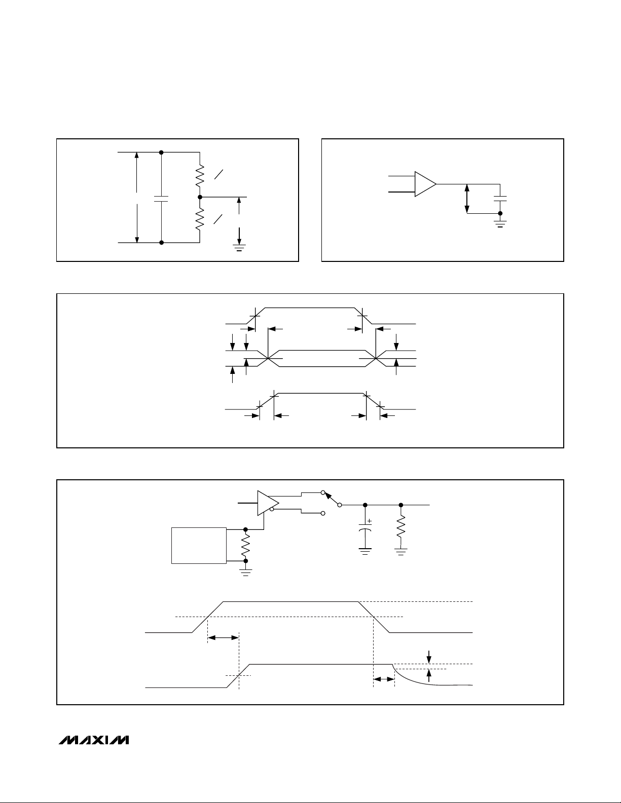
Enable times t
ZH
and tZL(see the
Switching Character-
istics
) assume the devices are not in a low-power shut-
down state. Enable times t
ZH(SHDN)
and t
ZL(SHDN)
assume the devices are in a shutdown state. It takes drivers and receivers longer to become enabled from lowpower shutdown mode (t
ZH(SHDN)
, t
ZL(SHDN)
) than from
driver-/receiver-disable mode (tZH, tZL).
Line Length
The RS-485 standard covers line lengths up to 4000ft.
For line lengths greater than 4000ft, use the repeater
application shown in Figure 8.
Typical Applications
The MAX13181E–MAX13184E transceivers are designed
for bidirectional data communications on multipoint bus
transmission lines. The MAX13181E/MAX13183E can be
used in either half-duplex or full-duplex configuration.
The MAX13182E/MAX13184E are for full-duplex only.
Figure 9 shows the typical network application circuit for
half-duplex, and Figures 10 and 11 show typical network
application circuits for full duplex.
To minimize reflections, terminate the line at both ends in
its characteristics impedance, and keep stub lengths off
the main line as short as possible. The slew-rate-limited
MAX13181E/MAX13182E are more tolerant of imperfect
termination.
MAX13181E–MAX13184E
+5.0V, ±15kV ESD-Protected, Half-Duplex/
Full-Duplex, RS-485 Transceiver in µDFN
______________________________________________________________________________________ 13
Figure 8. Line Repeater for MAX13181E–MAX13184E
Figure 9. Typical Half-Duplex RS-485 Network
120Ω
DI
D
DE
RO
V
CC
H/F
MAX13181E–MAX13184E
CONFIGURED FOR HALF-
R
DUPLEX OPERATION
B
BB
D
DI RO DE
DE
A
RO
*RE
DE
DI
(H/F)
(H/F for MAX13181E/
MAX13183E ONLY)
R
B
120Ω
Z
D
Y
120Ω
*RE FOR
MAX13182E/MAX13184E
(FULL DUPLEX)
120Ω
B
D
AAA
R
D
DI
R
RO
A
R
RERE
DATA IN
DATA OUT
DE
DI
RO
RE
Page 14

MAX13181E–MAX13184E
+5.0V, ±15kV ESD-Protected, Half-Duplex/
Full-Duplex, RS-485 Transceiver in µDFN
14 ______________________________________________________________________________________
Figure 10. Typical Full-Duplex RS-485 Network
Figure 11. Typical Full-Duplex RS-485 Network
RO
DE
DI
D
H/F
MAX13181E/MAX13183E
CONFIGURED FOR FULL-
DUPLEX OPERATION
A
R
B
Z
Y
120Ω
120Ω
YZBA
D
DI
DE
RE
R
RO
A
RO
DE
DI
R
D
B
Z
Y
120Ω
120Ω
YZBA
YZBA
R
D
DI
DE
RO
RE
YZBA
120Ω
120Ω
120Ω
120Ω
Y
D
Z
B
R
A
Y
D
Z
B
R
A
DI
DE
RE
RO
DI
DE
RE
RO
MAX13182E/MAX13184E
CONFIGURED FOR FULL-
DUPLEX OPERATION
R
D
DI
DE
RO
RE
D
DI
R
DE
RO
RE
Page 15

MAX13181E–MAX13184E
+5.0V, ±15kV ESD-Protected, Half-Duplex/
Full-Duplex, RS-485 Transceiver in µDFN
______________________________________________________________________________________ 15
Ordering Information (continued)
+
Denotes a lead-free package.
Chip Information
PROCESS: BiCMOS
Pin Configurations (continued)
MAX13182E
MAX13184E
1N.C. 14 V
CC
2RO 13 N.C.
3RE 12 A
4DE 11 B
5DI 10 Z
6GND 9Y
7GND 8 N.C.
TOP VIEW
SO
+
PART TEMP RANGE PIN-PACKAGE TOP MARK PKG CODE
MAX13183EELB+ -40°C to +85°C 10 µDFN ABA L1022-1
MAX13184EELB+ -40°C to +85°C 10 µDFN ABB L1022-1
MAX13184EESD+ -40°C to +85°C 14 SO — S14-1
Page 16

MAX13181E–MAX13184E
+5.0V, ±15kV ESD-Protected, Half-Duplex/
Full-Duplex, RS-485 Transceiver in µDFN
16 ______________________________________________________________________________________
Package Information
(The package drawing(s) in this data sheet may not reflect the most current specifications. For the latest package outline information,
go to www.maxim-ic.com/packages
.)
D
A
XXXX
XXXX
SAMPLE
MARKING
7
E
XXXX
PIN 1
INDEX AREA
b
A
A1
A2
L
L
e
C
L
e
EVEN TERMINAL
A A
(N/2 -1) x e)
b
N
1
C
L
e
ODD TERMINAL
SOLDER
MASK
COVERAGE
PIN 1
0.10x45∞
L1
6, 8, 10L UDFN.EPS
L
PACKAGE OUTLINE,
6, 8, 10L uDFN, 2x2x0.80 mm
-DRAWING NOT TO SCALE-
21-0164
1
A
2
Page 17

MAX13181E–MAX13184E
+5.0V, ±15kV ESD-Protected, Half-Duplex/
Full-Duplex, RS-485 Transceiver in µDFN
______________________________________________________________________________________ 17
Package Information (continued)
(The package drawing(s) in this data sheet may not reflect the most current specifications. For the latest package outline information,
go to www.maxim-ic.com/packages
.)
COMMON DIMENSIONS
SYMBOL MIN. NOM.
A
A1
A2
D 1.95 2.00
E
L
L1
PACKAGE VARIATIONS
PKG. CODE N e b
0.70 0.75
0.15 0.20 0.25
0.020 0.025 0.035
1.95 2.00
0.30 0.40
MAX.
0.80
2.05
-
2.05
0.50
0.10 REF.
6L622-1 0.65 BSC 0.30±0.05
0.25±0.050.50 BSC8L822-1
0.20±0.030.40 BSC10L1022-1
(N/2 -1) x e
1.30 REF.
1.50 REF.
1.60 REF.
-DRAWING NOT TO SCALE-
PACKAGE OUTLINE,
6, 8, 10L uDFN, 2x2x0.80 mm
21-0164
2
A
2
Page 18

MAX13181E–MAX13184E
+5.0V, ±15kV ESD-Protected, Half-Duplex/
Full-Duplex, RS-485 Transceiver in µDFN
Maxim cannot assume responsibility for use of any circuitry other than circuitry entirely embodied in a Maxim product. No circuit patent licenses are
implied. Maxim reserves the right to change the circuitry and specifications without notice at any time.
18
____________________Maxim Integrated Products, 120 San Gabriel Drive, Sunnyvale, CA 94086 408-737-7600
© 2007 Maxim Integrated Products is a registered trademark of Maxim Integrated Products, Inc.
SPRINGER
Package Information (continued)
(The package drawing(s) in this data sheet may not reflect the most current specifications. For the latest package outline information,
go to www.maxim-ic.com/packages
.)
N
HE
1
TOP VIEW
D
e
B
A
A1
C
L
FRONT VIEW
SIDE VIEW
INCHES
DIM
A1
B
C
e 0.050 BSC 1.27 BSC
E
H 0.2440.228 5.80 6.20
VARIATIONS:
D
D
0∞-8∞
MAX
MIN
0.069
0.053A
0.010
0.004
0.014
0.019
0.007
0.010
0.150
0.157
0.016L
0.050
INCHES
MAX
MINDIM
0.189 0.197 AA5.004.80 8
0.337 0.344 AB8.758.55 14
0.3940.386D
MILLIMETERS
MAX
MIN
1.35
1.75
0.10
0.25
0.35
0.49
0.19
0.25
3.80 4.00
0.40 1.27
MILLIMETERS
MAX
MIN
9.80 10.00
N MS012
16
AC
SOICN .EPS
PROPRIETARY INFORMATION
TITLE:
PACKAGE OUTLINE, .150" SOIC
REV.DOCUMENT CONTROL NO.APPROVAL
21-0041
1
B
1
 Loading...