

Page 1
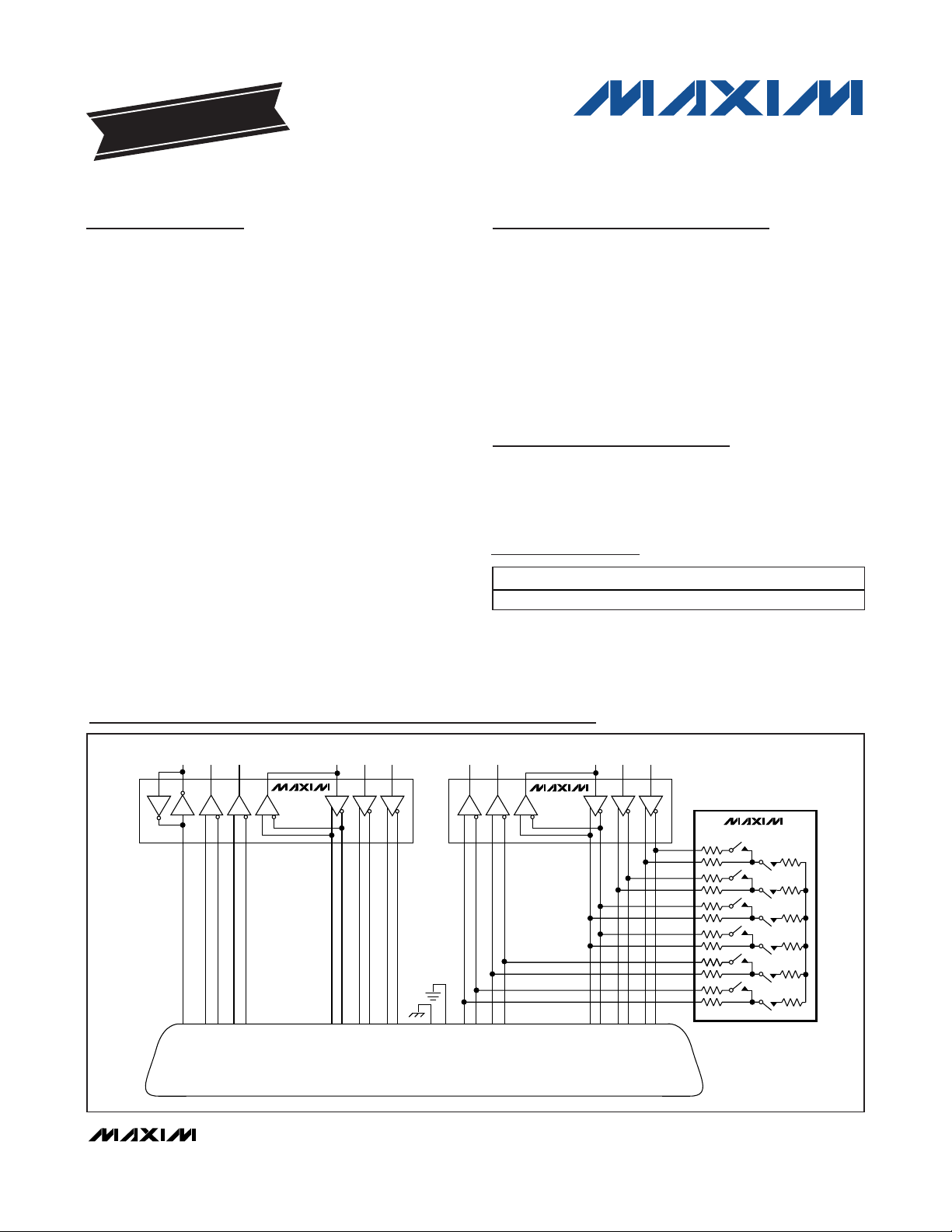
Typical Operating Circuit
For pricing, delivery, and ordering information, please contact Maxim Direct at 1-888-629-4642,
or visit Maxim's website at www.maxim-ic.com.
General Description
The MAX13174E contains six pin-selectable, multiprotocol cable termination networks. Each network is capable of terminating V.11 (RS-422, RS-530, RS-530A,
RS-449, V.36, and X.21) with a 100Ω differential load,
V.35 with a T-network load, or V.28 (RS-232) and V.10
(RS-423) with an open-circuit load for use with transceivers having on-chip termination. The termination protocol can be selected by the serial interface cable
wiring or by pin control. The MAX13174E replaces discrete resistor termination networks and expensive
relays required for multiprotocol termination, saving
space and cost.
The MAX13174E terminator is ideal to form a complete
+5V cable- or pin-selectable multiprotocol DCE/DTE
interface port when used with the MAX13170E and
MAX13172E transceiver ICs. The MAX13174E terminator can use the VEEpower generated by the
MAX13170E charge pump, simplifying system design.
The MAX13174E/MAX13170E/MAX13172E are pinfor-pin compatible with the MXL1344A/MXL1543/
MXL1544/MAX3175.
The MAX13174E is available in a 24-pin SSOP package
and is specified for the 0°C to +70°C commercial temperature range.
Features
♦ Supports V.11 and V.35 Termination
♦ Pin-Selectable Termination
♦ Pin-Selectable DCE/DTE Support
♦ Replaces Discrete Resistor Termination Networks
and Expensive Relays
♦ Available in 24-Pin SSOP Package
♦ Certified TBR-1 and TBR-2-Compliant Chipset
(NET1 and NET2)—Pending Completion of Testing
Applications
Data Networking PCI Cards
CSU and DSU Telecommunication Equipment
Data Routers Data Switches
MAX13174E
+5V Multiprotocol, Pin-Selectable
Cable Terminator
________________________________________________________________
Maxim Integrated Products
1
19-4742; Rev 0; 7/09
EVALUATION KIT
AVAILABLE
Ordering Information
Pin Configuration appears at end of data sheet.
+
Denotes a lead(Pb)-free/RoHS-compliant package.
PART TEMP RANGE PIN-PACKAGE
MAX13174ECAG+ 0°C to +70°C 24 SSOP
CTS DSR RTSDTRDCD
LL
T4
R4
13
18 5 10 8 22 6 23 20 19 4 1 7 16 3 9 17 12 15 11 24 14 2
CTS A (106)
DSR B
CTS B
LL A (141)
R2R3
DSR A (109)
MAX13172E
R1
T3
DCD A (107)
DCD B
DTR A (108)
DTR B
T1T2
RTS A (105)
RTS B
DB-25 CONNECTOR
RXD RXC TXDTXC SCTE
MAX13170E
R2R3
R1
RXC B
RXD A (104)
RXD B
SG (102)
SHIELD (101)
RXC A (115)
T3
TXC B
SCTE A (113)
SCTE B
TXC A (114)
T1T2
TXD B
TXD A (103)
MAX13174E
Page 2
MAX13174E
+5V Multiprotocol, Pin-Selectable
Cable Terminator
2 _______________________________________________________________________________________
ABSOLUTE MAXIMUM RATINGS
Stresses beyond those listed under “Absolute Maximum Ratings” may cause permanent damage to the device. These are stress ratings only, and functional
operation of the device at these or any other conditions beyond those indicated in the operational sections of the specifications is not implied. Exposure to
absolute maximum rating conditions for extended periods may affect device reliability.
(All voltages to GND, unless otherwise noted.)
Supply Voltages
V
CC
.......................................................................-0.3V to +6V
V
EE
.....................................................................+0.3V to -7.1V
Logic-Input Voltages
M0, M1, M2, DCE/DTE, LATCH............................-0.3V to +6V
Termination Network Inputs
R_A, R_B, R_C.....................................................-15V to +15V
R_A to R_B (high-impedance state) ................................±14V
R_A to R_B.........................................................................±6V
R_C to R_B (high-impedance state) ..................................±3V
R_A to R_C.........................................................................±3V
R_C to R_A (high-impedance state) ................................±14V
Continuous Power Dissipation (T
A
= +70°C)
24-Pin SSOP (derate 14.9mW/°C above +70°C) .......1196mW
Junction-to-Case Thermal Resistance (θ
JC
) (Note 1)
24-Pin SSOP..............................................................24.6°C/W
Junction-to-Ambient Thermal Resistance (θ
JA
) (Note 1)
24-Pin SSOP..............................................................66.9°C/W
Operating Temperature Range...............................0°C to +70°C
Junction Temperature......................................................+150°C
Storage Temperature Range .............................-65°C to +150°C
Lead Temperature (soldering, 10s) .................................+300°C
ELECTRICAL CHARACTERISTICS
(VCC= +4.5V to +5.5V, VEE= -4V to -7.1V, TA= 0°C to +70°C, unless otherwise noted. Typical values are at TA= +25°C, VCC= +5V,
V
EE
= -5V, unless otherwise noted.) (Note 2)
Note 1: Package thermal resistances were obtained using the method described in JEDEC specification JESD51-7, using a four-
layer board. For detailed information on package thermal considerations, refer to www.maxim-ic.com/thermal-tutorial
.
VCC Operating Range V
VEE Operating Range V
VCC POR Rising Threshold 1 1.88 2.75 V
VCC Supply Current
VEE Supply Current I
TERMINATOR INPUTS
Differential-Mode Impedance
V.35 Mode
Common-Mode Impedance
V.35 Mode
Differential-Mode Impedance
V.11 Mode
High-Impedance Leakage
Current
Differential Path Enable Time 50 µs
Differential Path Disable Time 300 µs
Common-Mode Path Enable Time 12 µs
Common-Mode Path Disable
PARAMETER SYMBOL CONDITIONS MIN TYP MAX UNITS
CC
EE
I
CC
I
CC_NOCABVEE
EE
I
All inputs connected to GND or VCC, except
no-cable mode
= 0V, M[x] = 1111 (Note 3) 1.34 2.85
All inputs connected to GND or VCC, except
no-cable mode
-2V ≤ V
-2V ≤ V
-7V ≤ VCM ≤ +7V, all channels, except nocable mode (Figure 1)
-7V ≤ V
mode, V
-15V ≤ V
Z
≤ +2V, all channels (Figure 1) 90 104 110 Ω
CM
≤ +2V, all channels (Figure 2) 135 153 165 Ω
CM
≤ +7V, all channels, no-cable
CM
= 0V, VAB ≤ 2V (Figure 1)
EE
≤ +15V -50 +50 µA
R_A
4.5 5 5.5 V
-7.1 -5 -4 V
2.2 6.15
-3.5 -1 mA
100 104 110
115
2µs
mA
Ω
Page 3
MAX13174E
+5V Multiprotocol, Pin-Selectable
Cable Terminator
_______________________________________________________________________________________ 3
Note 2: All parameters tested at a single temperature. Specifications over temperature are guaranteed by design.
Note 3: M[x] is the input bus DCE/DTE, M2, M1, M0.
ELECTRICAL CHARACTERISTICS (continued)
(VCC= +4.5V to +5.5V, VEE= -4V to -7.1V, TA= 0°C to +70°C, unless otherwise noted. Typical values are at TA= +25°C, VCC= +5V,
V
EE
= -5V, unless otherwise noted.) (Note 2)
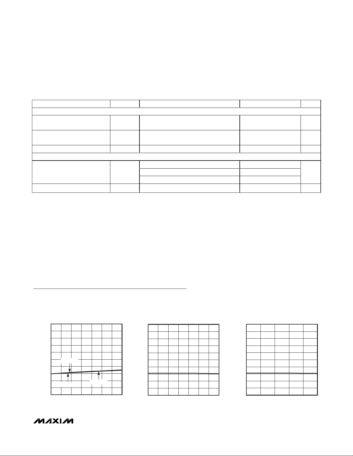
Typical Operating Characteristics
(VCC= +5V, VEE= -5V, TA = +25°C, unless otherwise noted.)
LOGIC INPUTS (M0, M1, M2, LATCH, DCE/DTE)
Input High Voltage V
Input Low Voltage V
Logic Input Current I
ESD PROTECTION
All Other Pins Human Body Model ±2 kV
PARAMETER SYMBOL CONDITIONS MIN TYP MAX UNITS
IH
IL
IN
VIN = VCC or GND -1 +1 µA
0.66 x
V
CC
0.33 x
V
CC
V
V
Human Body Model ±15
Air Gap Discharge IEC 61000-4-2 ±10R_A, R_B to GND
kV
Contact Discharge IEC 61000-4-2 ±6
V.11 OR V.35 DIFFERENTIAL IMPEDANCE
vs. TEMPERATURE
110
109
108
107
106
105
104
IMPEDANCE (I)
103
102
101
100
VCM = 0V
VCM = +7V
070
TEMPERATURE (NC)
VCM = -7V
MAX13174E toc01
605030 402010
V.11 OR V.35 DIFFERENTIAL IMPEDANCE
vs. COMMON-MODE VOLTAGE (V
110
109
108
107
106
105
104
IMPEDANCE (I)
103
102
101
100
-7 7
V.11 OR V.35 DIFFERENTIAL IMPEDANCE
vs. SUPPLY VOLTAGE (VCC)
5.3
5.14.94.74.5 5.5
VCC (V)
VCM (V)
)
CM
53-1 1-3-5
MAX13174E toc02
110
109
108
107
106
105
104
IMPEDANCE (I)
103
102
101
100
MAX13174E toc03
Page 4
MAX13174E
+5V Multiprotocol, Pin-Selectable
Cable Terminator
4 _______________________________________________________________________________________
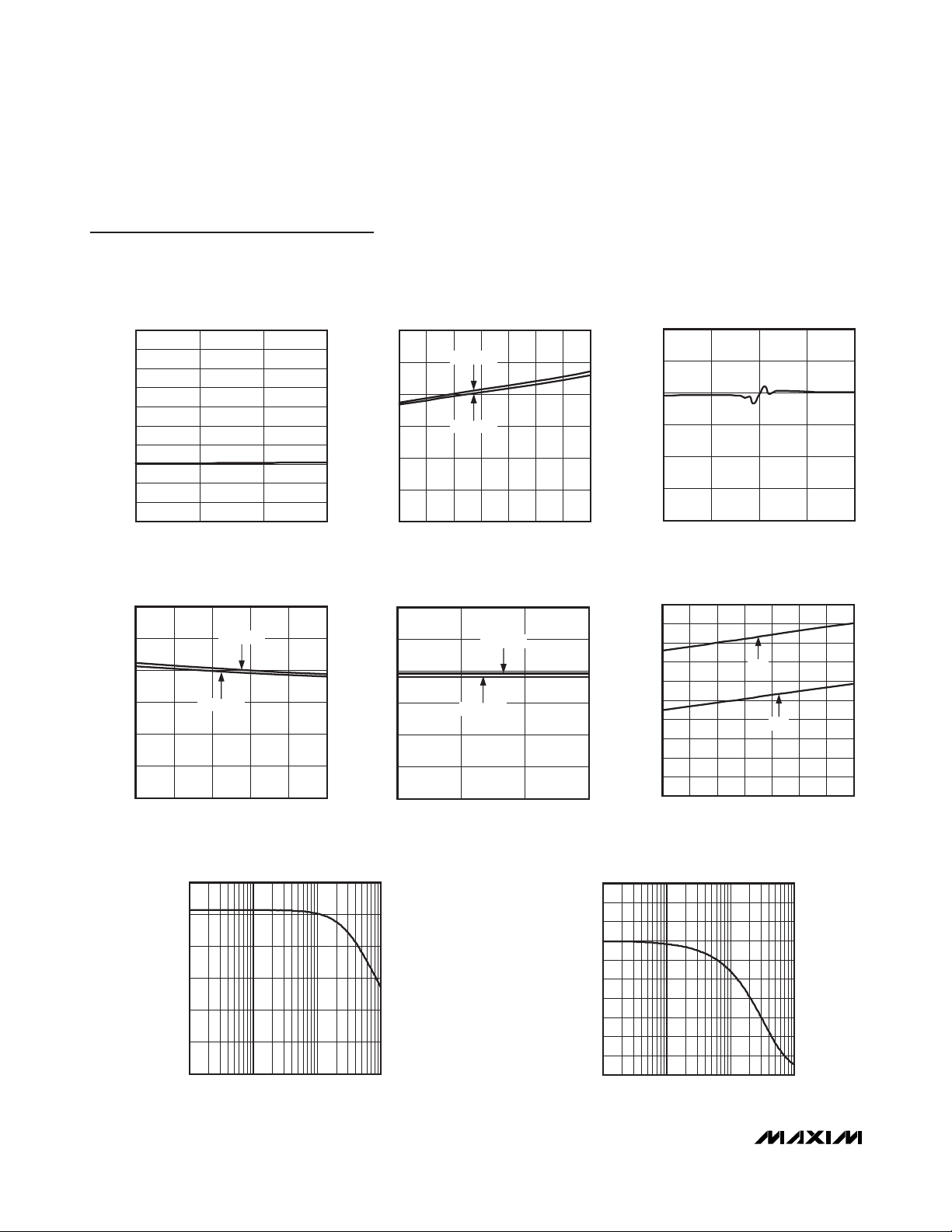
Typical Operating Characteristics (continued)
(VCC= +5V, VEE= -5V, TA = +25°C, unless otherwise noted.)
V.11 OR V.35 DIFFERENTIAL IMPEDANCE
vs. SUPPLY VOLTAGE (VEE)
110
109
108
107
106
105
104
IMPEDANCE (I)
103
102
101
100
VEE (V)
V.35 COMMON-MODE IMPEDANCE
vs. SUPPLY VOLTAGE (VCC)
165
160
155
150
IMPEDANCE (I)
145
140
135
VCM = +2V
VCM = -2V
V
CC
(V)
V.11 OR V.35 DIFFERENTIAL IMPEDANCE
MAGNITUDE vs. FREQUENCY
120
100
80
60
IMPEDANCE (I)
40
20
0
0.1 100
-5-6-7 -4
5.35.14.94.74.5 5.5
FREQUENCY (MHz)
101
MAX13174E toc04
MAX13174E toc07
V.35 COMMON-MODE IMPEDANCE
vs. TEMPERATURE
165
160
155
150
IMPEDANCE (I)
145
140
135
070
VCM = +2V
VCM = -2V
TEMPERATURE (
MAX13174E toc05
605040302010
NC)
V.35 COMMON-MODE IMPEDANCE
V.35 COMMON-MODE IMPEDANCE
vs. COMMON-MODE VOLTAGE (VCM)
165
160
155
150
IMPEDANCE (I)
145
140
135
HI-Z MODE SUPPLY CURRENT
vs. SUPPLY VOLTAGE (VEE)
MAX13174E toc08
1000
900
800
700
600
500
400
300
SUPPLY CURRENT (FA)
200
100
0
070
165
160
155
150
IMPEDANCE (I)
145
140
135
VCM = +2V
VCM = -2V
V
EE
-5-6-7 -4
(V)
V.11 OR V.35 DIFFERENTIAL IMPEDANCE
PHASE vs. FREQUENCY
15
10
MAX13174E toc10
5
0
-5
-10
-15
PHASE (DEGREES)
-20
-25
-30
-35
0.1 100
FREQUENCY (MHz)
(V)
V
CM
vs. TEMPERATURE
I
CC
I
EE
TEMPERATURE (NC)
101
MAX13174E toc06
10-1-2 2
MAX13174E toc09
605030 402010
MAX13174E toc11
Page 5

MAX13174E
+5V Multiprotocol, Pin-Selectable
Cable Terminator
_______________________________________________________________________________________ 5
Detailed Description
The MAX13174E contains six pin-selectable multiprotocol cable termination networks (Figure 3). Each network
is capable of terminating V.11 (RS-422, RS-530,
RS-530A, RS-449, V.36, and X.21) with a 100Ω differen-
tial load, V.35 with a T-network load, or V.28 (RS-232)
and V.10 (RS-423) with an open-circuit load for use with
transceivers that have on-chip termination. The termination protocol can be selected by the serial interface
cable wiring or by pin control. The MAX13174E
replaces discrete resistor termination networks and
expensive relays required for multiprotocol termination,
saving space and cost.
The MAX13174E terminator is designed to form a complete +5V cable- or pin-selectable multiprotocol DCE/DTE
interface port when used with the MAX13170E and
MAX13172E transceivers. The MAX13174E terminator
can use the VEEpower generated by the MAX13170E
charge pump, simplifying system design. The
MAX13174E/MAX13170E/MAX13172E are functionally
compatible with the MXL1344A/MXL1543/MXL1544/
MAX3175.
Termination Modes
The termination networks in the MAX13174E can be set
to one of three modes: V.11, V.35, or high impedance.
As shown in Figure 4, in V.11 mode, switch S1 is closed
and switch S2 is open, presenting 104Ω across terminals A and B. In V.35 mode, switches S1 and S2 are
both closed, presenting a T-network with 104Ω differen-
tial impedance and 153Ω common-mode impedance.
In high-impedance mode, switches S1 and S2 are both
open, presenting a high impedance across terminals A
and B suitable for V.28 and V.10 modes.
Pin Description
PIN NAME FUNCTION
1 M0 Mode-Select Input (Table 1)
2VEEN eg ati ve S up p l y V ol tag e ( typ i cal l y connected to V
3 R1C Load 1, Center Tap
4 R1B Load 1, Node B
5 R1A Load 1, Node A
6 R2A Load 2, Node A
7 R2B Load 2, Node B
8 R2C Load 2, Center Tap
9 R3A Load 3, Node A
10 R3B Load 3, Node B
11 R3C Load 3, Center Tap
12, 13 GND Ground
14 V
15 R4B Load 4, Node B
16 R4A Load 4, Node A
17 R5B Load 5, Node B
18 R5A Load 5, Node A
19 R6A Load 6, Node A
20 R6B Load 6, Node B
21 LATCH
22 DCE/DTE DCE/DTE Mode-Select Input (Table 1)
23 M2 Mode-Select Input (Table 1)
24 M1 Mode-Select Input (Table 1)
CC
+5V Supply Voltage. Bypass to GND with a 0.1µF capacitor.
Latch Signal Input. When LATCH is low, the input latches are transparent. When LATCH is high, the data
at the mode-select inputs are latched.
of M AX 13170E ) . Byp ass to GN D w i th a 0.1µF cap aci tor .
E E
Page 6

MAX13174E
+5V Multiprotocol, Pin-Selectable
Cable Terminator
6 _______________________________________________________________________________________
The state of the MAX13174E’s mode-select pins—M0,
M1, M2, and DCE/DTE—determines the mode of each of
the six termination networks. Table 1 shows a cross-reference of termination mode and select pin state for each of
the six termination networks within the MAX13174E.
No-Cable Mode
The MAX13174E enters no-cable mode when the modeselect inputs—M0, M1, and M2—are connected high. In
no-cable mode, all six termination networks are placed
in V.11 mode, with S1 closed and S2 open (Figure 4).
Applications Information
Older multiprotocol interface termination circuits have
been constructed using expensive relays with discrete
resistors, custom cables with built-in termination, or
complex circuit-board configurations to route signals to
the correct termination. The MAX13174E provides a
simple solution to this termination problem. All required
termination configurations are easily cable- or pinselectable using the four mode-control input pins (M0,
M1, M2, and DCE/DTE).
Using the MAX13174E in a Multiprotocol
Serial Interface
The MAX13174E terminator is designed to form a complete +5V cable- or pin-selectable multiprotocol
DCE/DTE interface port when used with the
MAX13170E/MAX13172E differential drivers/receivers.
The MAX13174E terminator is designed to use the V
EE
power generated by the MAX13171E’s charge pump
and meets all data sheet specifications when connected as illustrated in Figure 5. The mode-selection tables
of all three devices are identical, allowing the M0, M1,
M2, and DCE/DTE pins of each device to be connected
to a single 4-wire control bus. The MAX13170E and
MAX13172E provide internal pullups for the four lines,
Figure 3. Block Diagram
VCM = ±7V OR ±2V
V
DM
= ±2V
R
DM
=
V
DM
R2 = 52Ω
R3 = 127Ω
R1 = 52Ω
S1 ON
A
I
I
B
S2 OFF
AMMETER
Figure 1. V.11 or V.35 Differential Impedance Measurement
VCM = ±2V
R2 = 52Ω
R3 = 127Ω
R1 = 52Ω
S1 ON
A
B
S2 ON
AMMETER
R
CM
=
V
CM
I
I
Figure 2. V.35 Common-Mode Impedance Measurement
3 8 11 12 13
1
M0
MAX13174E
24
M1
23
22
21
M2
DCE/DTE
LATCH
V
CCVEE
123456
52
4 6 7 9 10 16 15 18 1714 19 20
Page 7

MAX13174E
+5V Multiprotocol, Pin-Selectable
Cable Terminator
_______________________________________________________________________________________ 7
forcing them to the logic-high state if they are not
grounded. This allows interface-mode configuration by
simply strapping the appropriate pins to ground in the
interconnect cable.
V.11 Termination
A standard V.11 interface is shown in Figure 6. For highspeed data transmission, the V.11 specification recommends terminating the cable at the receiver with a 100Ω
(min) resistor. The resistor, although not required, prevents reflections from corrupting transmitted data.
Note: Z indicates high impedance, 1 = high, and 0 = low. Z, V.11, and V.35 refer to termination modes (Figure 4).
Figure 4. Termination Modes
Table 1. Termination Mode Select Table
PROTOCOL DCE/ DTE M2 M1 M0 R1 R2 R3 R4 R5 R6
V.10/RS-423 0 0 0 0 Z Z Z Z Z Z
RS-530A 0 0 0 1 Z Z Z V.11 V.11 V.11
RS-530 0 0 1 0 Z Z Z V.11 V.11 V.11
X.21 0 0 1 1 Z Z Z V.11 V.11 V.11
V.35 0 1 0 0 V.35 V.35 Z V.35 V.35 V.35
RS-449/V.36 0 1 0 1 Z Z Z V.11 V.11 V.11
V.28/RS-232 0 1 1 0 Z Z Z Z Z Z
No Cable 0 1 1 1 V.11 V.11 V.11 V.11 V.11 V.11
V.10/RS-423 1 0 0 0 Z Z Z Z Z Z
RS-530A 1 0 0 1 Z Z Z Z V.11 V.11
RS-530 1 0 1 0 Z Z Z Z V.11 V.11
X.21 1 0 1 1 Z Z Z Z V.11 V.11
V.35 1 1 0 0 V.35 V.35 V.35 Z V.35 V.35
RS-449/V.36 1 1 0 1 Z Z Z Z V.11 V.11
V.28/RS-232 1 1 1 0 Z Z Z Z Z Z
No Cable 1 1 1 1 V.11 V.11 V.11 V.11 V.11 V.11
A
MAX13174E
R1
52Ω
A
MAX13174E MAX13174E
R1
52Ω
A
R1
52Ω
S1
CLOSED
C
S2
OPEN
R2
52Ω
B
R3
127Ω
B
S1
CLOSED
CLOSED
R2
52Ω
(a) V.11 (b) V.35 (c) Z
S1
OPEN
CC
S2
R3
127Ω
B
R2
52Ω
S2
OPEN
R3
127Ω
Page 8

MAX13174E
+5V Multiprotocol, Pin-Selectable
Cable Terminator
8 _______________________________________________________________________________________
Figure 5. Multiprotocol DCE/DTE Port
C7
DTE_TXD/DCE_RXD
DTE_SCTE/DCE_RXC
DTE_TXC/DCE_TXC
DTE_RXC/DCE_SCTE
DTE_RXD/DCE_TXD
C3
4.7μF
C6
100pF
100pF
3
V
CC
5V
C1
1μF
C4
4.7μF
10
11
12
13
14
3
1
2
4
5
6
7
8
9
MAX13170E
M0
M1
M2
DCE/DTE
CHARGE
PUMP
T1
T2
T3
R1
R2
R3
28
C2
1μF
27
26
C5
4.7μF
25
24
23
22
21
20
19
18
17
16
15
C13
1μF
C12
1μF
14
V
CC
2
V
EE
C8
100pF
8111213
4 6 7 9 10 16 15 18 17 19 20 22 23 24 15
MAX13174E
DCE/DTE
M2
M1
LATCH
M0
21
DCE
DTE
2
RXD A
TXD A
14
24
11
15
12
17
16
RXD B
TXD B
RXC A
SCTE A
RXC B
SCTE B
TXC A
TXC A
TXC B
TXC B
SCTE A
RXC A
9
SCTE B
RXC B
3
TXD A
RXD A
TXD B
RXD B
7
SG
1
SHIELD
C9
1μF
C10
1μF
DTE_RTS/DCE_CTS
DTE_DTR/DCE_DSR
DTE_DCD/DCE_DCD
DTE_DSR/DCE_DTR
DTE_CTS/DCE_RTS
DTE_LL/DCE_LL
DCE/DTE
M2
M1
M0
DB-25
4
19
20
23
8
10
6
22
5
13
18
CONNECTOR
RTS A
RTS B
DTR A
DTR B
DCD A
DCD B
DSR A
DSR B
CTS A
CTS B
LLA
CTS A
CTS B
DSR A
DSR B
DCD A
DCD B
DTR A
DTR B
RTS A
RTS B
LLA
V
CC
1
V
CC
2
V
DD
3
4
5
6
7
8
10
9
MAX13172E
11
M0
12
M1
13
M2
14
DCE/DTE
28
V
EE
27
GND
26
T1
25
24
T2
23
T3
22
21
R1
20
R2
19
18
R3
17
16
R4
T4
15
INVERT
C11
1μF
Page 9

MAX13174E
+5V Multiprotocol, Pin-Selectable
Cable Terminator
_______________________________________________________________________________________ 9
In Figure 7, the MAX13174E is used to terminate the
V.11 receiver on the MAX13170E. Internal to the
MAX13174E, S1 is closed and S2 is open to present a
104Ω typical differential resistance and high-Z common-mode impedance. The MAX13170E's internal V.28
termination is disabled by opening S3.
The V.11 specification allows for signals with commonmode variations of ±7V and differential signal amplitudes from 2V to 6V. The MAX13174E maintains
termination impedance between 100Ω and 110Ω over
these conditions.
V.35 Termination
Figure 8 shows a standard V.35 interface. The generator
and the load must both present a 100Ω ±10Ω differential
impedance and a 150Ω ±15Ω common-mode impedance. The V.35 driver generates a current output
(±11mA, typ) that develops an output voltage between
440mV and 660mV across the load termination networks.
In Figure 9, the MAX13174E is used to implement the
resistive T-network that is needed to properly terminate
the V.35 receiver. Internal to the MAX13174E, S1 and S2
are closed to connect the T-network resistors to the circuit.
The V.35 specification allows for ±4V of ground difference
between the V.35 generator and V.35 load. The
MAX13174E maintains correct termination impedance
over these conditions.
V.35 EMI reduction
For applications where EMI reduction is especially
important, the MAX13174E termination networks provide
a pin for shunting common-mode driver currents to
GND. Mismatches between the driver A and B output
propagation delays can create a common-mode disturbance on the cable. This common-mode energy can be
shunted to GND by placing a 100pF capacitor to GND
from the center tap of the T-network termination (R1C,
R2C, and R3C as shown in Figure 5).
V.28 Termination
Most industry-standard V.28 receivers (including the
MAX13170E and MAX13172E) do not require external
termination because the receiver includes an internal
5kΩ termination resistor. When the MAX13174E is
Figure 6. Typical V.11 Interface
Figure 7. V.11 Termination and Internal Resistance Networks
BALANCED
INTERCONNECTING
GENERATOR
CABLE
TERMINATION
A
B
C
A′
B′
C′
CABLE
100Ω
MIN
LOAD
RECEIVER
A′
R1
MAX13174E
52Ω
S1
R2
52Ω
B′
C′
R3
S2
124Ω
A
R5
55kΩ
R8
5kΩ
S3
B
GND
+
1.4V
R4
55kΩ
S2
-
11kΩ
11kΩ
R6
R7
MAX13170E
RECEIVER
S1
Page 10
MAX13174E
+5V Multiprotocol, Pin-Selectable
Cable Terminator
10 ______________________________________________________________________________________
placed in V.28 mode, all six of the termination networks
are placed in a high-Z mode. In high-Z mode, the
MAX13174E termination networks do not interfere with
the MAX13170E's internal 5kΩ termination.
In Figure 10, the MAX13174E and MAX13170E are
placed in V.28 mode. Switches S1 and S2 are opened
on the MAX13174E to place the network in high-Z
mode. Switch S3 is closed on the MAX13170E to
enable the 5kΩ terminating resistor.
A Complete X.21 Interface
A complete DTE-to-DCE interface operating in X.21
mode is shown in Figure 11. The MAX13174E terminates the V.11 clock and data signals. The MAX13170E
carries the clock and data signals, and the MAX13172E
carries the control signals. The control signals generally
do not require external termination.
ESD Protection
ESD-protection structures are incorporated on all pins
to protect against electrostatic discharges encountered
during handling and assembly. The differential resistors
Figure 8. Typical V.35 Interface
Figure 9. V.35 Termination and Internal Resistance Networks
50Ω
50Ω
A′
B′
GENERATOR
125Ω
S1
R1
52Ω
S2
R2
52Ω
MAX13174E
R3
124Ω
A
B
C
BALANCED
INTERCONNECTING
CABLE
A
B
R8
5kΩ
LOAD
CABLE
TERMINATION
A′
125Ω
B′
C′
R5
55kΩ
R6
11kΩ
S3
+
-
1.4V
R7
11kΩ
R4
55kΩ
S1
50Ω
50Ω
MAX13170E
RECEIVER
RECEIVER
C′
S2
GND
Page 11

MAX13174E
+5V Multiprotocol, Pin-Selectable
Cable Terminator
______________________________________________________________________________________ 11
have extra protection against static electricity. Maxim’s
engineers have developed state-of-the-art structures to
protect these pins against an ESD of ±15kV (Human
Body Model) without damage. The ESD structures withstand high ESD in all states: normal operation, shutdown, and powered down. After an ESD event, the
MAX13174E keeps working without latchup or damage.
ESD protection can be tested in various ways. The
Electrical Characteristics
table shows the limits, and
each device is characterized for protection to the following methods:
• Human Body Model
• Contact Method specified in IEC 61000-4-2
• Air Gap Discharge Method specified in IEC 61000-4-2
ESD Test Conditions
ESD performance depends on a variety of conditions.
Contact Maxim for a reliability report that documents
test setup, test methodology, and test results.
Human Body Model
Figure 12a shows the Human Body Model, and Figure
12b shows the current waveform it generates when discharged into a low impedance. This model consists of a
100pF capacitor charged to the ESD voltage of interest,
which is then discharged into the test device through a
1.5kΩ resistor.
IEC 61000-4-2
The IEC 61000-4-2 standard covers ESD testing and
the performance of finished equipment. However, it
does not specifically refer to integrated circuits. The
MAX13174E helps equipment designs to meet IEC
61000-4-2 without the need for additional ESD-protection components.
The major difference between tests done using the
Human Body Model and IEC 61000-4-2 is higher peak
current in IEC 61000-4-2 because series resistance is
lower in the IEC 61000-4-2 model. Figure 12c shows
the IEC 61000-4-2 model, and Figure 12d shows the
current waveform for the IEC 61000-4-2 ESD Contact
Discharge test.
Compliance Testing
A European Standard EN 45001 test report for the
MAX13170E, MAX13172E, and MAX13174E chipset will
be available from Maxim upon completion of testing.
Contact Maxim Quality Assurance for a copy of the report.
Figure 10. V.28 Termination and Internal Resistance Networks
A′
R1
MAX13174E
52Ω
S1
R3
S2
124Ω
R2
52Ω
B′
C′
A
R5
55kΩ
R8
5kΩ
S3
B
GND
+
1.4V
R4
55kΩ
S2
-
11kΩ
11kΩ
R6
R7
S1
MAX13170E
RECEIVER
Page 12

MAX13174E
+5V Multiprotocol, Pin-Selectable
Cable Terminator
12 ______________________________________________________________________________________
Figure 11. DTE-to-DCE X.21 Interface
SERIAL
CONTROLLER
TXD
SCTE
TXC
RXC
RXD
RTS
DTR
DCD
DSR
DTE
D1
D2
D3
R1
R2
R3
MAX13172E
D1
D2
D3
R1
R2
DCE
MAX13174EMAX13170E
104Ω
TXD
104Ω
SCTE
104Ω
104Ω
104Ω
TXC
RXC
RXD
RTS
DTR
DCD
DSR
MAX13170EMAX13174E
R3
R2
R1
D3
D2
D1
MAX13172E
R3
R2
R1
D3
D2
SERIAL
CONTROLLER
TXD
SCTE
TXC
RXC
RXD
RTS
DTR
DCD
DSR
CTS
LL
R3
D4
R4
CTS
LL
D1
R4
D4
CTS
LL
Page 13

MAX13174E
+5V Multiprotocol, Pin-Selectable
Cable Terminator
SPRINGER
Maxim cannot assume responsibility for use of any circuitry other than circuitry entirely embodied in a Maxim product. No circuit patent licenses are
implied. Maxim reserves the right to change the circuitry and specifications without notice at any time.
Maxim Integrated Products, 120 San Gabriel Drive, Sunnyvale, CA 94086 408-737-7600 ____________________
13
© 2009 Maxim Integrated Products Maxim is a registered trademark of Maxim Integrated Products, Inc.
Figure 12b. Human Body Current Waveform
Figure 12a. Human Body ESD Test Model
Figure 12d. IEC 61000-4-2 ESD Generator Current Waveform
Figure 12c. IEC 61000-4-2 ESD Test Model
24
23
22
21
20
19
18
17
1
2
3
4
5
6
7
8
M1
M2
R1B
R1C
V
EE
M0
TOP VIEW
R6B
R6A
R5A
R5BR2C
R2B
R2A
R1A
16
15
14
13
9
10
11
12
R4A
R4B
V
CC
GND
GND
R3C
R3B
R3A
SSOP
MAX13174E
LATCH
DCE/DTE
+
Pin Configuration
Chip Information
PROCESS: BiCMOS
PACKAGE TYPE PACKAGE CODE DOCUMENT NO.
24 SSOP A24+3
21-0056
Package Information
For the latest package outline information and land patterns, go
to www.maxim-ic.com/packages
.
HIGH-
VOLTAGE
DC
SOURCE
R
C
1MΩ
CHARGE-CURRENT
LIMIT RESISTOR
C
100pF
s
R
D
1500Ω
DISCHARGE
RESISTANCE
STORAGE
CAPACITOR
HIGH-
VOLTAGE
DC
SOURCE
R
C
50MΩ TO 100MΩ
CHARGE-CURRENT
LIMIT RESISTOR
C
150pF
s
R
D
330Ω
DISCHARGE
RESISTANCE
STORAGE
CAPACITOR
DEVICE
UNDER
DEVICE
UNDER
TEST
TEST
I
R
t
DL
PEAK-TO-PEAK RINGING
(NOT DRAWN TO SCALE)
AMPS
IP 100%
90%
36.8%
10%
0
0
t
RL
TIME
CURRENT WAVEFORM
I
100%
90%
PEAK
I
10%
tR = 0.7ns TO 1ns
30ns
60ns
t
 Loading...