

General Description
The MAX13172E is a four-driver/four-receiver multiprotocol transceiver that operates from a single +5V supply in
conjunction with the MAX13170E and MAX13174E. The
MAX13172E, along with the MAX13170E and the
MAX13174E, form a complete software-selectable data
terminal equipment (DTE) or data communication equipment (DCE) interface port that supports the V.28 (RS-232),
V.10/V.11 (RS-449/V.36, EIA-530, EIA-530A, X.21, RS-
423), and V.35 protocols. The MAX13172E transceiver
carries serial-interface control signaling, while the
MAX13170E carries the high-speed clock and data signals. Typically, the MAX13170E is terminated using the
MAX13174E.
The MAX13172E is available in a 5.3mm x 10.2mm, 28pin SSOP package and operates over the 0°C to +70°C
commercial temperature range.
Applications
Data Networking
CSU/DSU Devices
Data Routers
Switches
PCI Cards
Telecommunication Equipment
Features
♦ The MAX13170E/MAX13172E/MAX13174E Chipset
is a Pin-for-Pin Upgrade to the MXL1544/MAX3175/
MXL1543/MXL1543B Chipset
♦ Chipset Operates from a Single +5V Supply
♦ Software-Selectable DCE/DTE Configurations
♦ Supports V.28 (RS-232), V.10/V.11 (RS-449/V.36,
EIA-530, EIA-530A, X.21, RS-423) Protocols
♦ Flowthrough Pin Configuration
♦ Fail-Safe Receivers While Maintaining V.11 and
V.35 Compatibility
♦ Extremely Low Maximum Shutdown Current
(No-Cable Mode)
♦ TUV-Certified NET1/NET2 and TBR1/TBR2
Compliant (Pending)
♦ Extended ESD Protection for All Transmitter
Outputs and Receivers Inputs to GND
±10kV Using the Human Body Model
±3kV Using the Contact Method Specified in
IEC 61000-4-2
±3kV Using the Air Gap Discharge Method
Specified in IEC 61000-4-2
MAX13172E
+5V Multiprotocol, Software-Selectable
Clock Transceiver
________________________________________________________________
Maxim Integrated Products
1
Ordering Information
19-3900; Rev 0; 05/08
PART
TEMP RANGE
PIN-PACKAGE
MAX13172ECAI+
0°C to +70°C
28 SSOP
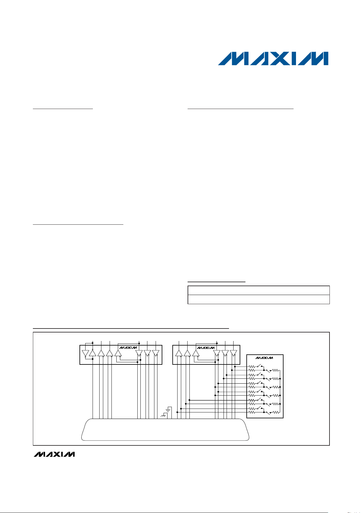
Typical Operating Circuit
T1T2
T3
T4
R1
R2R3
MAX13170E
RXD RXC TXDTXC SCTE
T1T2
T3
R1
R2R3
MAX13172E
CTS DSR RTSDTRDCD
RXC B
RXD A (104)
RXD B
SG (102)
SHIELD (101)
RTS A (105)
RTS B
DTR A (108)
DTR B
DCD A (107)
DCD B
DSR A (109)
CTS A (106)
DSR B
CTS B
LL A (141)
TXD B
SCTE A (113)
SCTE B
TXC A (114)
TXC B
TXD A (103)
DB-25 CONNECTOR
13
R4
LL
RXC A (115)
18 5 10 8 22 6 23 20 19 4 1 7 16 3 9 17 12 15 11 24 14 2
MAX13174E
+
Denotes a lead-free package.
Pin Configuration appears at end of data sheet.
For pricing, delivery, and ordering information, please contact Maxim Direct at 1-888-629-4642,
or visit Maxim’s website at www.maxim-ic.com.
MAX13172E
+5V Multiprotocol, Software-Selectable
Clock Transceiver
2 _______________________________________________________________________________________
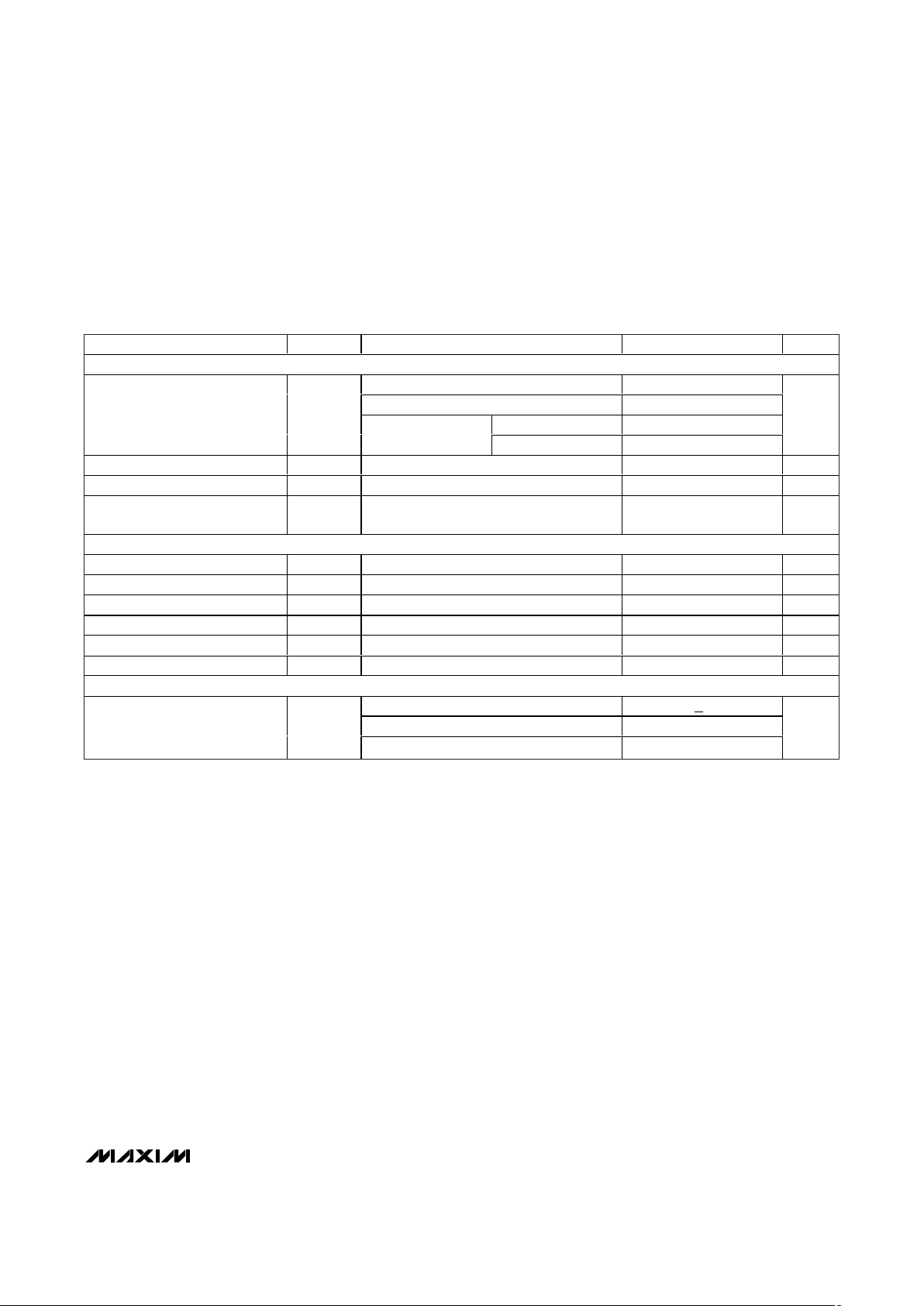
ABSOLUTE MAXIMUM RATINGS
ELECTRICAL CHARACTERISTICS
(V
CC
= 4.5V to 5.5V, TA= T
MIN
to T
MAX
. Typical values are at VCC= 5V, and TA= +25°C, V.28 mode only: VDD= +5.6V to +7.1V and
V
EE
= -7.1V to -5.4V. Typical values are at VDD= +6.9V and VEE= -6.7V, no-cable mode: VDD= VCCand VEE= 0, other modes: V
DD
= +5.15V to +5.7V and VEE= -4.84V to -4.16V. Typical value are at VDD= +5.3V and VEE= -4.5V.) (Notes 2, 3)
Stresses beyond those listed under “Absolute Maximum Ratings” may cause permanent damage to the device. These are stress ratings only, and functional
operation of the device at these or any other conditions beyond those indicated in the operational sections of the specifications is not implied. Exposure to
absolute maximum rating conditions for extended periods may affect device reliability.
(All voltages referenced to GND, unless otherwise noted.)
Supply Voltages
V
CC
.......................................................................-0.3V to +6V
V
DD
....................................................................-0.3V to +7.1V
V
EE
.....................................................................+0.3V to -7.1V
V
DD
to VCC............................................................+0.3 to +6V
Logic Input Voltages
M0, M1, M2, DCE/DTE, T_IN, INVERT..................-0.3V to +6V
Logic Output Voltages
R_OUT....................................................-0.3V to (V
CC
+ 0.3V)
Transmitter Outputs
T_OUT_, T_OUT_/R_IN_ (No-Cable Mode,
V.28 only).........................................................-15V to +15V
Short-Circuit Duration to GND...............................Continuous
Receiver Inputs
R_IN_, T_OUT_/R_IN_ ........................................-15V to +15V
R_INA to R_INB, T3OUTA/R1INA to
T3OUT/R1INB.....................................................-15V to +15V
Continuous Power Dissipation (T
A
= +70°C)
28-Pin SSOP (derate 9.5mW/°C above +70°C) ...........762mW
Junction-to-Case Thermal Resistance (θ
JC
) (Note 1)
28-Pin SSOP ................................................................25°C/W
Junction-to-Ambient Thermal Resistance (θ
JA
) (Note 1)
28-Pin SSOP ................................................................67°C/W
Operating Temperature Range ................................0°C to 70°C
Junction Temperature .....................................................+150°C
Storage Temperature Range ............................-65°C to +150°C
Lead Temperature (soldering, 10s) ................................+300°C
PARAMETER SYMBOL CONDITIONS MIN TYP MAX UNITS
VCC Operating Range V
CC
4.5 5.5 V
V.28 mode 5.6 7.1
VDD Operating Range V
DD
V.10 or V.11 mode 5.15 5.7
V
V.28 mode -7.1 -5.4
VEE Operating Range V
EE
V.10 or V.11 mode -4.84 -4.16
V
CH1, CH3 = V.11, CH2 = V.10, CH4 = V.10,
no load
5.5
CH1, CH3 = V.11, CH2 = V.10, CH4 = V.10,
full load
95 135
C H 1, C H 2, C H 3 = V .11, C H 4 = V .10, ful l l oad 138 180
V.28 mode 3.5 9
mA
VCC Supply Current (DCE Mode)
(Digital Inputs = GND or V
CC
)
(Transmitter Outputs Static)
I
CC
No cable mode; M0, M1, M2, DCE/DTE,
INVERT, open or at V
CC
(VDD = VCC and
V
EE
= GND)
010µA
C H 1, C H 3 = V .11, C H 2, C H 4 = V .10, no l oad 300
Internal Power Dissipation
(DCE Mode)
P
D
V.28 mode, full load 54
mW
Note 1: Package thermal resistances were obtained using the method described in JESD51-7, using a four-layer board. For detailed
information on package thermal considerations, refer to www.maxim-ic.com/thermal-tutorial
.
MAX13172E
+5V Multiprotocol, Software-Selectable
Clock Transceiver
_______________________________________________________________________________________ 3
ELECTRICAL CHARACTERISTICS (continued)
(V
CC
= 4.5V to 5.5V, TA= T
MIN
to T
MAX
. Typical values are at VCC= 5V, and TA= +25°C, V.28 mode only: VDD= +5.6V to +7.1V and
V
EE
= -7.1V to -5.4V. Typical values are at VDD= +6.9V and VEE= -6.7V, no-cable mode: VDD= VCCand VEE= 0, other modes: V
DD
= +5.15V to +5.7V and VEE= -4.84V to -4.16V. Typical value are at VDD= +5.3V and VEE= -4.5V.) (Notes 2, 3)
PARAMETER SYMBOL CONDITIONS MIN TYP MAX UNITS
CH1, CH3 = V.11, CH2 = V.10 or V.11,
CH4 = V.10, no load
2.1
CH1, CH2, CH3 = V.11, CH4 = V.10,
full load (output low)
13 30
CH1, CH3 = V.11, CH2, CH4 = V.10,
full load (output low)
22 30
V.28 mode, no load 1
V.28 mode, full load (output low) 12 18
mA
VEE Supply Current I
EE
No cable mode
(V
DD
= VCC and VEE = GND)
010µA
CH1, CH3 = V.11, CH2 = V.10 or V.11,
CH4 = V.10, no load
0.6
CH1, CH2, CH3 = V.11, CH4 = V.10,
full load (output high)
11 30
CH1, CH3 = V.11, CH2, CH4 = V.10, full
load (output high)
22 30
V.28 mode, no load 2.5
V.28 mode, full load (output high) 12 10
mA
VDD Supply Current I
DD
No cable mode
(V
DD
= VCC and VEE = GND)
010µA
Thermal-Shutdown Protection THSD +145 °C
LOGIC INPUTS (M0, M1, M2, DCE/DTE, INVERT, T1IN, T2IN, T3IN, T4IN)
Input High Voltage V
IH
0.66 x V
C C
V
Input Low Voltage V
IL
0.33 x V
C C
V
Logic-Input Current I
IN
T1IN, T2IN, T3IN, T4IN -1 +1 µA
Pullup Resistor R
PUIN
M0, M1, M2, DCE/DTE, INVERT to V
CC
50 100 166 kΩ
LOGIC OUTPUTS (R1OUT, R2OUT, R3OUT, R4OUT)
Output High Voltage V
OH
I
SOURCE
= 4mA 0.66 x V
C C
V
Output Low Voltage V
OL
I
SINK
= 4mA 0.33 x V
C C
V
Output Pullup Resistor R
PUY
No cable mode (to VCC) 71.4 kΩ
Transmitter Output Leakage
Current
I
Z
-0.25V < V
OUT
< +0.25V, VCC = 0 or no
cable mode
±1 ±5 µA
V.11 TRANSMITTER
Open-Circuit Differential Output
Voltage
V
ODO
Open circuit, R = 1.95kΩ, Figure 1 - V
CC
+V
CC
V
R = 50Ω, Figure 1 0.5 x V
OD O
Loaded Differential Output
Voltage (Note 4)
|V
ODL
|
R = 50Ω, Figure 1 2
V
Change in Magnitude of Output
Differential Voltage
ΔV
OD
R = 50Ω, Figure 1 0.2 V
MAX13172E
+5V Multiprotocol, Software-Selectable
Clock Transceiver
4 _______________________________________________________________________________________
ELECTRICAL CHARACTERISTICS (continued)
(V
CC
= 4.5V to 5.5V, TA= T
MIN
to T
MAX
. Typical values are at VCC= 5V, and TA= +25°C, V.28 mode only: VDD= +5.6V to +7.1V and
V
EE
= -7.1V to -5.4V. Typical values are at VDD= +6.9V and VEE= -6.7V, no-cable mode: VDD= VCCand VEE= 0, other modes: V
DD
= +5.15V to +5.7V and VEE= -4.84V to -4.16V. Typical value are at VDD= +5.3V and VEE= -4.5V.) (Notes 2, 3)
PARAMETER SYMBOL CONDITIONS MIN TYP MAX UNITS
Common-Mode Output Voltage V
OC
R = 50Ω, Figure 1 3.0 V
Change in Magnitude of
Common-Mode Output Voltage
ΔV
OC
R = 50Ω, Figure 1 0.2 V
Short-Circuit Current I
SC
V
OUT
= GND 150 mA
Rise Time t
R
Figures 2, 5 4 10 ns
Fall Time t
F
Figures 2, 5 6 10 ns
Transmitter Input-to-Output Prop
Delay
t
PHL
, t
PLH
Figures 2, 5 22 ns
Data Skew |t
PHL-tPLH
| Figures 2, 5 (Note 5) 3 ns
Output-to-Output Skew t
SKEWT
Figures 2, 5 (Notes 5, 6) 3 ns
V.11 RECEIVER
Differential Threshold Voltage V
TH
-7V ≤ VCM ≤ +7V -200 -50 mV
Input Hysteresis ΔV
TH
-7V ≤ VCM ≤ +7V 15 mV
Receiver Input Current I
IN
-10V ≤ V
A,B
≤ +10V -0.66 +0.66 mA
Receiver Input Resistance R
IN
-10V ≤ V
A,B
≤ +10V 15 30 kΩ
Rise or Fall Time tR, t
F
Figures 2, 6 3 ns
Receiver Input-to-Output Delay t
PHL
, t
PLH
Figures 2, 6 16 26 ns
Data Skew |t
PHL-tPLH
| Figures 2, 6 (Note 5) 3.5 ns
Output-to-Output Skew t
SKEWR
(Notes 5, 6) 3.5 ns
V.10 TRANSMITTER
RL = 3.9kΩ (out high) 4 6
Open-Circuit Output Voltage
Swing (Figure 3)
V
O
RL = 3.9kΩ (out low) -6 -4
V
RL = 450Ω (out high) 3.6
RL = 450Ω (out low) -3.6
Output Voltage Swing (Figure 3) V
T
RL = 450Ω 0.9 x |V
O
|
V
Short-Circuit Current I
SC
VO = GND -55 +55 mA
Rise or Fall Time tR, t
F
RL = 450Ω, CL =100pF (Figure 7) 2 µs
Transmitter Input-to-Output Delay t
PLH, tPHLRL
= 450Ω, CL =100pF (Figure 7) 1 µs
V.10 RECEIVER
Input Threshold Voltage V
TH
Measured on inverting input (A) 50 250 mV
Input Hysteresis ΔV
TH
25 mV
Receiver Input Current I
IN
-10V ≤ VA ≤ +10V -0.66 +0.66 mA
Receiver Input Impedance R
IN
-10V ≤ VA ≤ +10V 15 30 kΩ
Rise or Fall Time tR, t
F
Figures 4, 8 3 ns
Receiver Input-to-Output Delay
from Low to High
t
PLH
Figures 4, 8 55 ns
Receiver Input-to-Output Delay
from High to Low
t
PHL
Figures 4, 8 109 ns
Data Skew |t
PHL-tPLH
| Figures 4, 8 60 ns
MAX13172E
+5V Multiprotocol, Software-Selectable
Clock Transceiver
_______________________________________________________________________________________ 5
ELECTRICAL CHARACTERISTICS (continued)
(V
CC
= 4.5V to 5.5V, TA= T
MIN
to T
MAX
. Typical values are at VCC= 5V, and TA= +25°C, V.28 mode only: VDD= +5.6V to +7.1V and
V
EE
= -7.1V to -5.4V. Typical values are at VDD= +6.9V and VEE= -6.7V, no-cable mode: VDD= VCCand VEE= 0, other modes: V
DD
= +5.15V to +5.7V and VEE= -4.84V to -4.16V. Typical value are at VDD= +5.3V and VEE= -4.5V.) (Notes 2, 3)
PARAMETER SYMBOL CONDITIONS MIN TYP MAX UNITS
V.28 TRANSMITTER
Open circuit (output high) V
DD
Open circuit (output low) V
EE
Output high +5 +6.8
Output-Voltage Swing V
OD
RL = 3kΩ
Output low -6.8 -5
V
Short-Circuit Current |ISC| 85 mA
Output Slew Rate SR
R/F
RL = 3kΩ, CL = 2500pF, Figures 3, 9 4 30 V/µs
Transmitter Input-to-Output
Propagation Delay
t
PHL, tPLHRL
= 3kΩ, CL = 2500pF, Figures 3, 9 1 2 µs
V.28 RECEIVER
Input Threshold Low V
IL
0.8 V
Input Threshold High V
IH
2V
Input Hysteresis V
HYST
0.25 V
Input Resistance R
IN
-15V ≤ VIN ≤ +15V 3 5 7 kΩ
Rise or Fall Time tR, t
F
Figures 4, 10 3 ns
Receiver Input-to-Output Delay t
PHL, tPLH
Figures 4, 10 150 ns
ESD PROTECTION (T_OUT_, T_OUT_/R_OUT_, R_IN_ to GND)
Contact Discharge IEC61000-4-2 + 3
Air Gap Discharge IEC61000-4-2 ±3
ESD Protection
Human Body Model ±10
kV
Note 2: The MAX13172E is designed to operate with VDDand VEEsupplied by the MAX13170E charge pump.
Note 3: All devices are 100% production tested at T
A
= +25°C, and are guaranteed by design for TA = 0°C to +70°C as specified.
Note 4: |V
ODL
| is guaranteed at both 0.5 x V
ODO
and 2V.
Note 5: Guaranteed by design, not production tested.
Note 6: Ouput-to-output skews are evaluated as a difference of propagation delays between different channels in the same condtion
and for the same polarity (LH or HL).
MAX13172E
+5V Multiprotocol, Software-Selectable
Clock Transceiver
6 _______________________________________________________________________________________
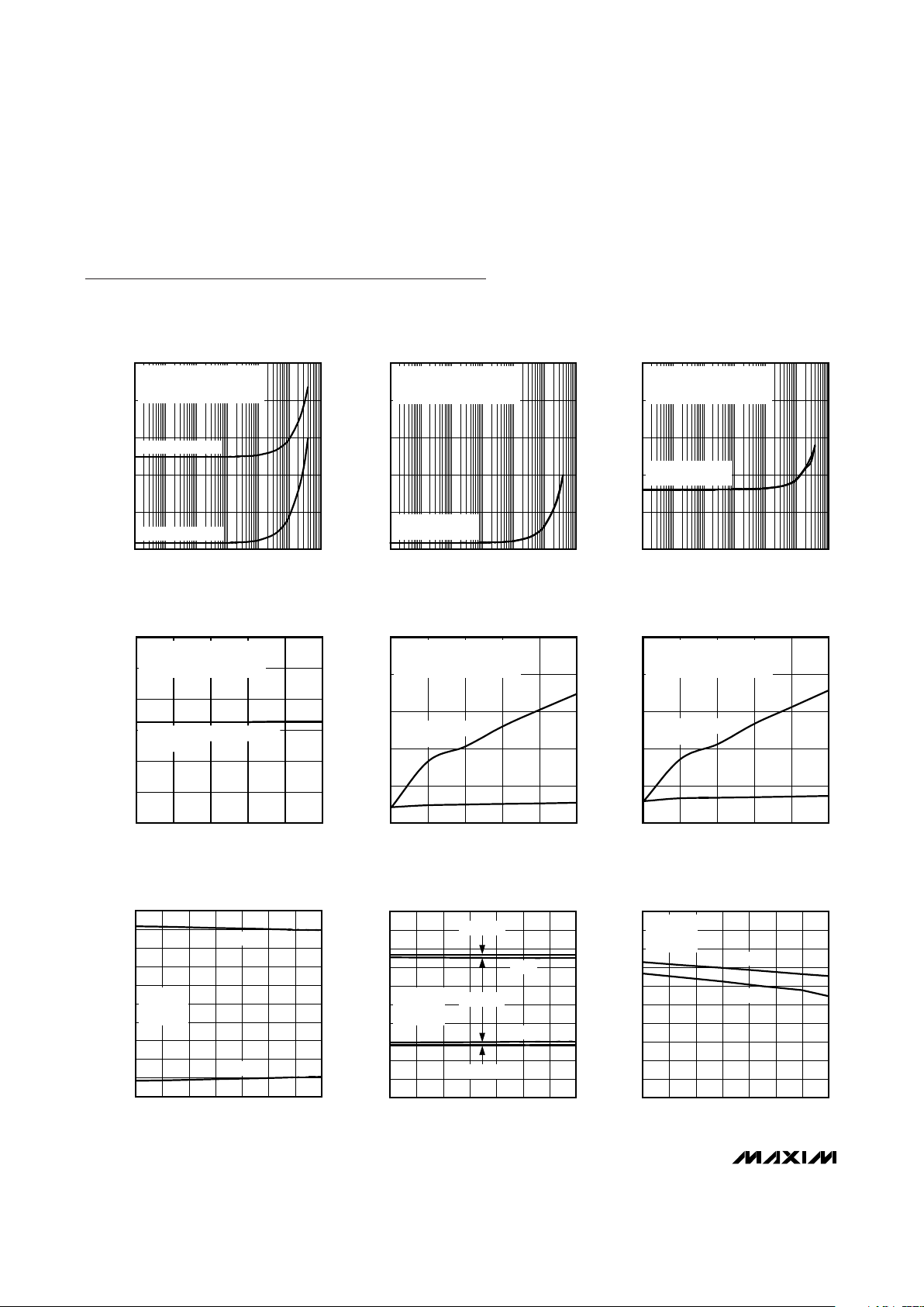
Typical Operating Characteristics
(TA = +25°C, unless otherwise noted.)
V.11 MODE SUPPLY CURRENT (ICC)
vs. DATA RATE
DATA RATE (kbps)
0.1 100 1,000 10,0001 10 100,000
I
CC
(mA)
0
250
50
100
150
200
MAX13172E toc01
DCE MODE, INVERT = 1
ALL TRANSMITTERS OPERATING
AT THE SPECIFIED DATA RATE
FULL LOAD, R = 50
Ω
NO LOAD, R = 1.95k
Ω
V.11 MODE SUPPLY CURRENT (IDD)
vs. DATA RATE
DATA RATE (kbps)
0.1 100 1,000 10,0001 10 100,000
I
DD
(mA)
0
10
2
4
6
8
MAX13172E toc02
DCE MODE, INVERT = 1
ALL TRANSMITTERS OPERATING
AT THE SPECIFIED DATA RATE
FULL LOAD, R = 50
Ω
NO LOAD, R = 1.95k
Ω
V.11 MODE SUPPLY CURRENT (IEE)
vs. DATA RATE
DATA RATE (kbps)
0.1 100 1,000 10,0001 10 100,000
I
EE
(mA)
0
10
2
4
6
8
MAX13172E toc03
DCE MODE, INVERT = 0
ALL TRANSMITTERS OPERATING
AT THE SPECIFIED DATA RATE
FULL LOAD, R = 50
Ω
NO LOAD, R = 1.95k
Ω
0
1
4
3
2
5
6
010050 150 200 250
V.28 MODE SUPPLY CURRENT (ICC)
vs. DATA RATE
MAX13172E toc04
DATA RATE (kbps)
I
CC
(mA)
DCE MODE, INVERT = 0
ALL TRANSMITTERS OPERATING
AT THE SPECIFIED DATA RATE
FULL LOAD (RL = 3kΩ,CL = 2500pF)
AND NO LOAD
0
4
12
8
16
20
0 10050 150 200 250
V.28 MODE SUPPLY CURRENT (IDD)
vs. DATA RATE
MAX13172E toc05
DATA RATE (kbps)
I
DD
(mA)
DCE MODE, INVERT = 0
ALL TRANSMITTERS OPERATING
AT THE SPECIFIED DATA RATE
FULL LOAD, RL = 3kΩ,
C
L
= 2500pF
0
4
12
8
16
20
0 10050 150 200 250
V.28 MODE SUPPLY CURRENT (IEE)
vs. DATA RATE
MAX13172E toc06
DATA RATE (kbps)
I
EE
(mA)
DCE MODE, INVERT = 0
ALL TRANSMITTERS OPERATING
AT THE SPECIFIED DATA RATE
FULL LOAD, RL = 3kΩ,
C
L
= 2500pF
-5
-2
-3
-4
0
-1
4
3
2
1
5
0 10203040506070
V.11 LOADED DRIVER DIFFERENTIAL
OUTPUT VOLTAGE vs. TEMPERATURE
MAX13172E toc07
TEMPERATURE (°C)
DRIVER DIFFERENTIAL OUTPUT VOLTAGE (V)
V
OUT+
V
OUT-
DCE MODE,
INVERT = 1,
R = 50
Ω
-10
-4
-6
-8
0
-2
8
6
4
2
10
0 10203040506070
V.10 OUTPUT VOLTAGE
vs. TEMPERATURE
MAX13172E toc08
TEMPERATURE (°C)
OUTPUT VOLTAGE (V)
V
OUT+
V
OUT-
DCE MODE,
V
DD
= +5.3V,
V
EE
= -4.5V
RL = 3.9k
Ω
RL = 450
Ω
RL = 3.9kΩ
0.80
0.86
0.84
0.82
0.90
0.88
0.98
0.96
0.94
0.92
1.00
0 10203040506070
V.10 RATIO OF LOADED/UNLOADED
OUTPUT VOLTAGE vs. TEMPERATURE
MAX13172E toc09
TEMPERATURE (°C)
RATIO (V/V)
V
OUT+
V
OUT-
DCE MODE,
V
DD
= +5.3V,
V
EE
= -4.5V
MAX13172E
+5V Multiprotocol, Software-Selectable
Clock Transceiver
_______________________________________________________________________________________ 7
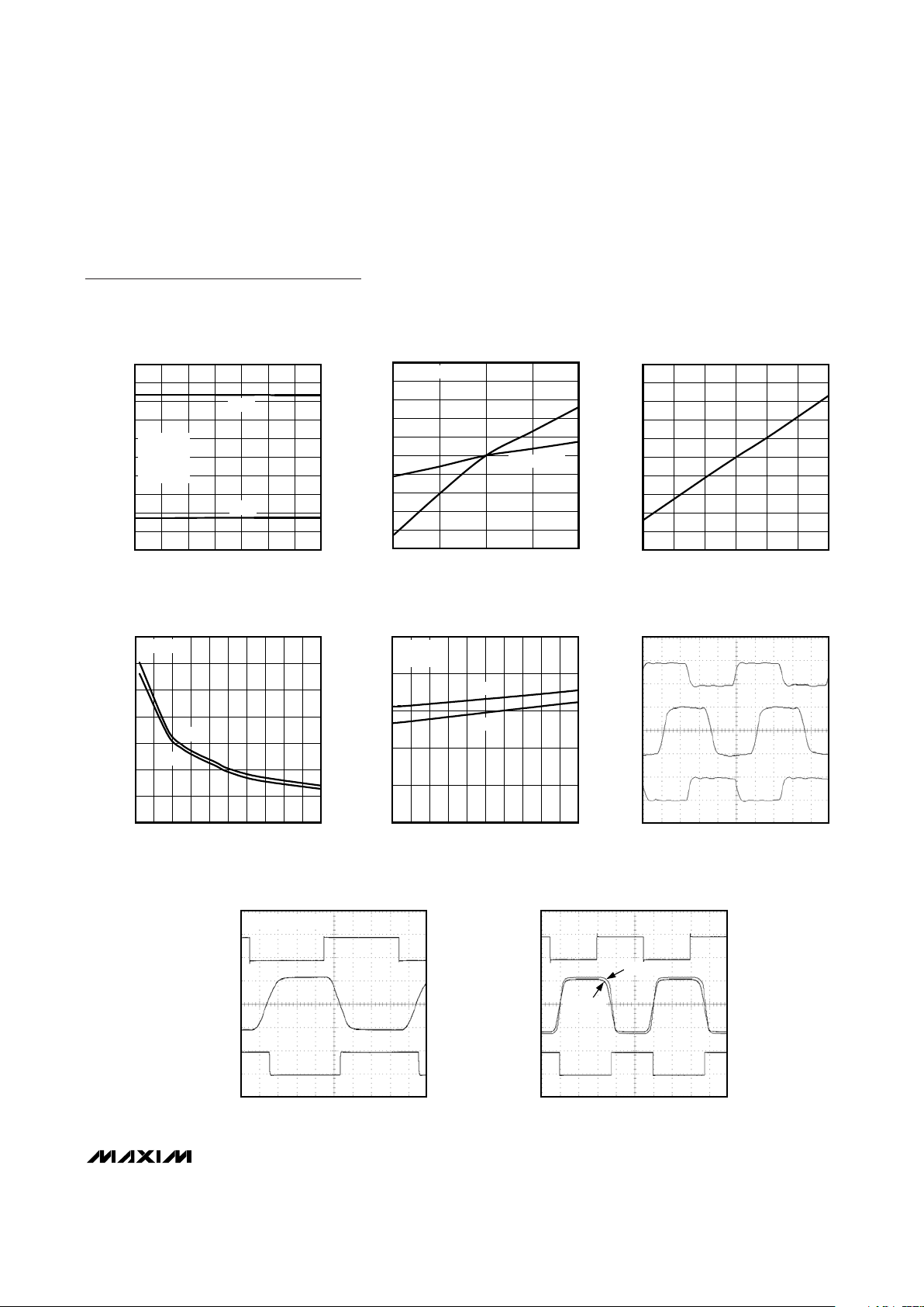
Typical Operating Characteristics (continued)
(TA = +25°C, unless otherwise noted.)
-10
-4
-6
-8
0
-2
8
6
4
2
10
0 10203040506070
V.28 LOADED OUTPUT VOLTAGE
vs. TEMPERATURE
MAX13172E toc10
TEMPERATURE (°C)
OUTPUT VOLTAGE (V)
DCE MODE,
R = 3k
Ω,
V
DD
= +6.9V,
V
EE
= -6.7V
V
OUT+
V
OUT-
-500
-300
-400
-100
-200
100
0
200
400
300
500
-10 0 5-5 10
V.11 RECEIVER INPUT CURRENT
vs. INPUT VOLTAGE
MAX13172E toc11
INPUT VOLTAGE (V)
INPUT CURRENT (μA)
DTE MODE
R1IN_
R2IN_, R3IN_
-5
-3
-4
-1
-2
1
0
2
4
3
5
-15 0 5 10-5-10 15
V.28 RECEIVER INPUT CURRENT
vs. INPUT VOLTAGE
MAX13172E toc12
INPUT VOLTAGE (V)
INPUT CURRENT (mA)
0
10
5
20
15
30
25
35
02K1K 3K 4K 5K
V.28 SLEW RATE
vs. LOAD CAPACITANCE
MAX13172E toc13
500 2.5K1.5K 3.5K 4.5K
LOAD CAPACITANCE (pF)
SLEW RATE (V/μs)
RL = 3k
Ω
SRF
SRR
0
2.0
1.6
0.8
0.4
1.2
0 400200 600 800 1,000
V.10 TEANSMITTER RISE/FALL TIME
vs. LOAD CAPACITANCE
MAX13172E toc14
100 500300 700 900
LOAD CAPACITANCE (pF)
RISE/FALL TIME (μs)
VDD = +5.3V,
V
EE
= -4.5V
FALL
RISE
LOOPBACK SCOPE SHOT PHOTO V.11
MODE (UNLOADED)
MAX13172E toc15
10ns/div
R
OUT
T
OUT/RIN
T
IN
5V/div
5V/div
5V/div
LOOPBACK SCOPE SHOT PHOTO V.28
MODE (LOADED)
MAX13172E toc16
1μs/div
R
OUT
T
OUT/RIN
T
IN
5V/div
5V/div
5V/div
RL = 3kΩ,CL = 2500pF
LOOPBACK SCOPE SHOT PHOTO V.10
MODE (LOADED)
MAX13172E toc17
4μs/div
R
OUT
T
OUT/RIN
T
IN
5V/div
5V/div
5V/div
RL = 450
Ω
RL = 3.9k
Ω

MAX13172E
+5V Multiprotocol, Software-Selectable
Clock Transceiver
8 _______________________________________________________________________________________
Pin Description
PIN NAME FUNCTION
1V
CC
Device Supply Voltage. Bypass VCC with a 1µF capacitor-to-ground as close as possible to the
device.
2V
DD
Positive Supply Voltage Input. VDD is generated by the MAX13170E. Bypass VDD with a 1µF
capacitor to ground.
3 T1IN Transmitter 1 Logic Input
4 T2IN Transmitter 2 Logic Input
5 T3IN Transmitter 3 Logic Input
6 R1OUT Receiver 1 Logic Output
7 R2OUT Receiver 2 Logic Output
8 R3OUT Receiver 3 Logic Output
9 T4IN Transmitter 4 Logic Output
10 R4OUT Receiver 4 Logic Output
11 M0 Mode Select 0 Input. Internally pullup to VCC.
12 M1 Mode Select 1 Input. Internally pullup to VCC.
13 M2 Mode Select 2 Input. Internally pullup to VCC.
14
DCE/DTE
DCE/DTE Input. Internally pullup to VCC. Logic level high selects DCE interface.
15 INVERT T4/R4 Select Input. Internally pullup to VCC. INVERT reverses the action of DCE/DTE for Channel 4.
16
T4OUTA/
R4INA
Transmitter 4 Output/Inverting Receiver Input
17 R3INB Receiver 3 Noninverting Input
18 R3INA Receiver 3 Inverting Input
19 R2INB Receiver 2 Noninverting Input
20 R2INA Receiver 2 Inverting Input
21
T3OUTB/
R1INB
Transmitter 3 Noninverting Output/Receiver 1 Noninverting Input
22
T3OUTA/
R1INA
Transmitter 3 Inverting Output/Receiver 1 Inverting Input
23 T2OUTB Transmitter 2 Noninverting Output
24 T2OUTA Transmitter 2 Inverting Output
25 T1OUTB Transmitter 1 Noninverting Output
26 T1OUTA Transmitter 1 Inverting Output
27 GND Ground
28 V
EE
Negative Supply Input. VEE is generated by the MAX13170E. Bypass VEE with a 1µF capacitor to
ground.

MAX13172E
V
OC
R
R
V
OD
Figure 1. V.11 DC Test Circuit
C
L
R
L
V
O
TA
Figure 3. V.10/V.28 Transmitter Test Circuit
100pF
15pF
100pF
100
Ω
T
A
B
B
A
R
Figure 2. V.11 AC Test Circuit
15pF
TAR
Figure 4. V.10/V.28 Receiver Test Circuit
Test Circuits
+5V Multiprotocol, Software-Selectable
Clock Transceiver
_______________________________________________________________________________________ 9
Detailed Description
The MAX13172E is a four-driver/four-receiver, multiprotocol transceiver that operates from a single +5V supply. The charge pump operates from the MAX13170E.
The MAX13172E along with the MAX13170E and
MAX13174E, form a complete software-selectable
DTE or DCE interface port that supports the V.28
(RS-232), V.10/V.11 (RS-449/V.36, EIA-530, EIA-530A,
X.21, RS-423), and V.35 protocols. The MAX13172E
usually carries the control signals. The MAX13170E
carries the high-speed clock and data signals, and the
MAX13174E provides termination for the clock and
data signals.
The MAX13172E features an ultra-low supply current
no-cable mode, fail-safe operation, and thermal-shut-
down circuitry. Thermal shutdown protects the transmitter and receiver outputs against excessive power dissipation. When activated, the thermal-shutdown circuitry
places the driver outputs into a high-impedance state.
The state of the mode-select inputs M0, M1, and M2
determines which serial-interface protocol is selected
(Table 1). The state of the DCE/DTE input determines
whether the transceivers are configured as a DTE serial
port or a DCE serial port. When the DCE/DTE input is
logic-high, driver T3 is activated and receiver R1 is disabled. When the DCE/DTE input is logic-low, driver T3
disabled and receiver R1 is activated. The INVERT
input state changes the DCE/DTE functionality regarding T4 and R4 only. M0, M1, M2, INVERT, and
DCE/DTE are internally pulled up to V
CC
to ensure
logic-high if left unconnected.

MAX13172E
+5V Multiprotocol, Software-Selectable
Clock Transceiver
10 ______________________________________________________________________________________
+1V
-1V
V
0H
V
0L
A -B
R
0
INPUT
OUTPUT
0
t
PLH
t
PHL
f = 1MHz: tr, tf ≤ 1ns
VCC/2
V
CC
/2
90%
10%
t
R
90%
10%
t
F
0
t
PHL
0
V
0H
-V
0L
TIN_
A
10%
90%
tF
0
t
PLH
90%
10%
t
R
tR, tF ≤ 10ns
V
CC
/2 VCC/2
V
CC
Figure 6. V.11 Receiver Propagation Delays
Figure 7. V.10 Transmitter Propagation Delays
V
IH
V
IL
V
0H
V
0L
A
R
0
t
PHL
0
t
PLH
tR, tF ≤ 10ns
VCC/2
V
CC
/2
90%
10%
t
F
90%
10%
t
R
Figure 8. V.10 Receiver Propogation Delays
VCC/2
90%
10%
50%
t
PLH
V
CC
0
V
0
-V
0
TIN_
A - B
t
R
VCC/2
t
PHL
90%
10%
50%
t
F
f = 1MHz: tr, tf ≤ 1ns
Figure 5. V.11 Transmitter Propogation Delays
Switching Time Waveforms

MAX13172E
PROTOCOL M2 M1 M0
DCE/
DTE
INVERT T1 T2 T3 R1 R2 R3 T4 R4
Not Used
(Default V.11)
0 0 0 0 0 V.11 V.11 Z V.11 V.11 V.11 Z V.10
RS-530A 0 0 1 0 0 V.11 V.10 Z V.11 V.10 V.11 Z V.10
RS-530 0 1 0 0 0 V.11 V.11 Z V.11 V.11 V.11 Z V.10
X.21 0 1 1 0 0 V.11 V.11 Z V.11 V.11 V.11 Z V.10
V.35 1 0 0 0 0 V.28 V.28 Z V.28 V.28 V.28 Z V.28
RS-449/V.36 1 0 1 0 0 V.11 V.11 Z V.11 V.11 V.11 Z V.10
V.28/RS-232 1 1 0 0 0 V.28 V.28 Z V.28 V.28 V.28 Z V.28
No Cable 1 1 1 0 0 Z Z Z Z Z Z Z Z
Not Used
(Default V.11)
0 0 0 0 1 V.11 V.11 Z V.11 V.11 V.11 V.10 Z
RS-530A 0 0 1 0 1 V.11 V.10 Z V.11 V.10 V.11 V.10 Z
RS-530 0 1 0 0 1 V.11 V.11 Z V.11 V.11 V.11 V.10 Z
X.21 0 1 1 0 1 V.11 V.11 Z V.11 V.11 V.11 V.10 Z
V.35 1 0 0 0 1 V.28 V.28 Z V.28 V.28 V.28 V.28 Z
RS-449/V.36 1 0 1 0 1 V.11 V.11 Z V.11 V.11 V.11 V.10 Z
V.28/RS-232 1 1 0 0 1 V.28 V.28 Z V.28 V.28 V.28 V.28 Z
No Cable 1 1 1 0 1 Z Z Z Z Z Z Z Z
Table 1. Mode Select Table
+5V Multiprotocol, Software-Selectable
Clock Transceiver
______________________________________________________________________________________ 11
V
IH
V
IL
(2.0V)
(-0.3V)
V
0H
V
0L
A
R
1.3V
t
PHL
1.3V
t
PLH
tR, tF ≤ 10ns
VCC/2
V
CC
/2
90%
10%
t
F
90%
10%
t
R
Figure 10. V.28 Receiver Propogation Delays
Switching Time Waveforms (continued)
0
t
PHL
0
V
0H
-V
0L
TIN_
A
-3V
3V
tF
SRF = 6/t
F
SRR = 6/t
R
0
t
PLH
3V
-3V
t
R
tR, tF ≤ 10ns
V
CC
/2 VCC/2
V
CC
Figure 9. V.28 Transmitter Propagation Delays

MAX13172E
+5V Multiprotocol, Software-Selectable
Clock Transceiver
12 ______________________________________________________________________________________
The MAX13172E’s mode can be selected through software control of the M0, M1, M2, INVERT, and DCE/DTE
inputs. Alternatively, the mode can be selected by
shorting the appropriate combination of mode control
inputs to GND (the inputs left unconnected will be internally pulled up to VCC- logic-high). If the M0, M1, and
M2 mode inputs are all unconnected, the MAX13172E
will enter no-cable mode.
Fail-Safe
The MAX13172E guarantees a logic-high receiver output when the receiver inputs are shorted, or when they
are connected to a terminated transmission line with all
the drivers disabled. The V.11 receivers threshold is set
between -200mV and -50mV to guarantee fail-safe operation. If the differential receiver input voltage (B - A) is ≥
-50mV, ROUT is logic-high. In the case of a terminated
bus with all transmitters disabled, the receiver’s differential input voltage is pulled to 0 by the termination. With
the receiver thresholds of the MAX13172E, this results in
ROUT logic-high.
The V.10 receiver threshold is set between +50mV and
+250mV. If the V.10 receiver input voltage is less than or
equal to +250mV, ROUT is logic-high. The V.28 receiver
threshold is set between 0.8V and 2.0V. If the receiver input
voltage is less than or equal to 0.8V, ROUT is logic-high. In
the case of a terminated bus with transmitters disabled, the
receiver’s input voltage is pulled to 0 by the termination.
ESD Protection
As with all Maxim devices, a minimum of ±2kV-to-GND
ESD-protection structures are incorporated on all pins
to protect against electrostatic discharges encountered
during handling and assembly. The driver outputs and
receiver inputs of the MAX13172E have extra protection
against static electricity. Maxim’s engineers have
developed state-of-the-art structures to protect these
pins against ESD of ±10kV without damage (HBM). The
ESD structures withstand high ESD in all states: normal
operation, shutdown, and powered down. After an ESD
event, the MAX13172E keeps working without latchup
or damage. ESD protection can be tested in various
ways. The transmitter outputs and receiver inputs of the
MAX13172E are characterized for protection to the following limits:
• ±10kV using the Human Body Model
• ±3kV using the Contact Method specified in IEC
61000-4-2
• ±3kV using the Air Gap Discharge Method speci-
fied in IEC 61000-4-2
ESD Test Conditions
ESD performance depends on a variety of conditions.
Contact Maxim for a reliability report that documents
test setup, test methodology, and test results.
PROTOCOL M2 M1 M0
DCE/
DTE
INVERT T1 T2 T3 R1 R2 R3 T4 R4
Not Used
(Default V.11)
0 0 0 1 0 V.11 V.11 V.11 Z V.11 V.11 V.10 Z
RS-530A 0 0 1 1 0 V.11 V.10 V.11 Z V.10 V.11 V.10 Z
RS-530 0 1 0 1 0 V.11 V.11 V.11 Z V.11 V.11 V.10 Z
X.21 0 1 1 1 0 V.11 V.11 V.11 Z V.11 V.11 V.10 Z
V.35 1 0 0 1 0 V.28 V.28 V.28 Z V.28 V.28 V.28 Z
RS-449/V.36 1 0 1 1 0 V.11 V.11 V.11 Z V.11 V.11 V.10 Z
V.28/RS-232 1 1 0 1 0 V.28 V.28 V.28 Z V.28 V.28 V.28 Z
No Cable 1 1 1 1 0 Z Z Z Z Z Z Z Z
Not Used
(Default V.11)
0 0 0 1 1 V.11 V.11 V.11 Z V.11 V.11 Z V.10
RS-530A 0 0 1 1 1 V.11 V.10 V.11 Z V.10 V.11 Z V.10
RS-530 0 1 0 1 1 V.11 V.11 V.11 Z V.11 V.11 Z V.10
X.21 0 1 1 1 1 V.11 V.11 V.11 Z V.11 V.11 Z V.10
V.35 1 0 0 1 1 V.28 V.28 V.28 Z V.28 V.28 Z V.28
RS-449/V.36 1 0 1 1 1 V.11 V.11 V.11 Z V.11 V.11 Z V.10
V.28/RS-232 1 1 0 1 1 V.28 V.28 V.28 Z V.28 V.28 Z V.28
No Cable 1 1 1 1 1 Z Z Z Z Z Z Z Z
Table 1. Mode Select Table (continued)

MAX13172E
+5V Multiprotocol, Software-Selectable
Clock Transceiver
______________________________________________________________________________________ 13
Human Body Model
Figure 11a shows the Human Body Model, and Figure
11b shows the current waveform it generates when discharged into a low impedance. This model consists of
a 100pF capacitor charged to the ESD voltage of interest, which is then discharged into the test device
through a 1.5kΩ resistor.
IEC 61000-4-2
The IEC 61000-4-2 standard covers ESD testing and
performance of finished equipment. However, it
does not specifically refer to integrated circuits.
The MAX13172E helps equipment designs meet IEC
61000-4-2, without the need for additional ESD-protection components.
The major difference between tests done using the
Human Body Model and IEC 61000-4-2 is higher peak
current in IEC 61000-4-2 because series resistance is
lower in the IEC 61000-4-2 model. Hence, the ESD
withstand voltage measured to IEC 61000-4-2 is generally lower than that measured using the Human Body
Model. Figure 11c shows the IEC 61000-4-2 model,
and Figure 11d shows the current waveform for the IEC
61000-4-2 ESD Contact Discharge test.
CHARGE-CURRENT
LIMIT RESISTOR
DISCHARGE
RESISTANCE
STORAGE
CAPACITOR
C
s
150pF
R
C
50MΩ TO 100M
Ω
R
D
330
Ω
HIGH-
VOLTAGE
DC
SOURCE
DEVICE
UNDER
TEST
Figure 11c. IEC 61000-4-2 ESD Test Model
tr = 0.7ns TO 1ns
30ns
60ns
t
100%
90%
10%
I
PEAK
I
Figure 11d. IEC 61000-4-2 ESD Generator Current Waveform
CHARGE-CURRENT
LIMIT RESISTOR
DISCHARGE
RESISTANCE
STORAGE
CAPACITOR
C
s
100pF
R
C
1M
Ω
R
D
1500
Ω
HIGH-
VOLTAGE
DC
SOURCE
DEVICE
UNDER
TEST
Figure 11a. Human Body ESD Test Model
IP 100%
90%
36.8%
t
RL
TIME
t
DL
CURRENT WAVEFORM
PEAK-TO-PEAK RINGING
(NOT DRAWN TO SCALE)
I
r
10%
0
0
AMPS
Figure 11b. Human Body Current Waveform

MAX13172E
+5V Multiprotocol, Software-Selectable
Clock Transceiver
14 ______________________________________________________________________________________
Applications Information
Cable-Selectable Configuration
Application
A cable-selectable, multiprotocol DTE/DCE interface is
shown in Figure 12. The mode control lines M0, M1,
and DCE/DTE are wired to the DB-25 connector. To
select the serial-interface mode, the appropriate combination of M0, M1, M2, and DCE/DTE are grounded
within the cable wiring. The control lines that are not
grounded are pulled high by the internal pullups on the
MAX13170E. The serial-interface protocol of the
MAX13172E is now selected based on the cable that is
connected to the DB-25 interface.
V.10 (RS-423) Interface
The V.10 interface (Figure 13) is an unbalanced singleended interface capable of driving a 450Ω load. The
V.10 driver generates a minimum VOvoltage of ±4V
across A’ and C’ when unloaded and a minimum voltage of 0.9 ✕VOwhen loaded with 450Ω. The V.10
receiver has a single-ended input and does not reject
common-mode differences between C and C’. The V.10
receiver input trip threshold is defined between
+250mV and -250mV with input impedance characteristic shown in Figure 14.
The MAX13172E V.10 mode receiver has a threshold
between +50mV and +250mV. To ensure that the
receiver has proper fail-safe operation see the
Fail-Safe
section. To aid in rejecting system noise, the
MAX13172E V.10 receiver has a typical hysteresis of
25mV. Switch S3 in Figures 16a and 16b is open in
V.10 mode to disable the V.28 5kΩ termination at the
receiver input. Switch S2 is closed and switch S1 is
open to internally ground the receiver B input.
V.11 (RS-422) Interface
As shown in Figure 16, the V.11 protocol is a fully balanced differential interface. The V.11 driver generates a
minimum of ±2V between nodes A and B when 100Ω
minimum resistance is presented at the load. The V.11
receiver is sensitive to differential signals of ±200mV at
receiver inputs A’ and B’. The V.11 receiver input must
comply with the impedance curve of Figure 14 and reject
common-mode signals developed across the cable
(referenced from C to C’ in Figure 16) of up to ±7V.
The MAX13172E V.11 mode receiver has a differential
threshold between -50mV and -200mV. To ensure that
the receiver has proper fail-safe operation; see the
Fail-
Safe
section. To aid in rejecting system noise, the
MAX13172E V.11 receiver has a typical hysteresis of
15mV. Switch S3 in Figure 17 is open in V.11 mode to
disable the V.28 5kΩ termination at the inverting receiver input. Because the control signals are slow (60kbps),
100Ω termination resistance is generally not required for
the MAX13172E. The receiver inputs must also be compliant with the impedance curve shown in Figure 14.
V.28 (RS-232) Interface
The V.28 interface is an unbalanced single-ended interface (Figure 13). The V.28 generator provides a minimum of ±5V across the 3kΩ load impedance between
A’ and C’. The V.28 receiver has a single-ended input.
The MAX13172E V.28 mode receiver has a threshold
between +0.8V and +2.0V. To aid in rejecting system
noise, the MAX13172E V.28 receiver has a typical hysteresis of 0.25V. Switch S3 in Figures 18a and 18b is
closed in V.28 mode to enable the 5kΩ V.28 termination
at the receiver inputs.
No-Cable Mode
The MAX13172E will enter no-cable mode when the
mode-select pins are left unconnected or connected
high (M0 = M1 = M2 = 1). In this mode, the multiprotocol drivers and receivers are disabled and the supply
current is less than 10µA. The receiver outputs enter a
high-impedance state in no-cable mode, which allows
these output lines to be shared with other receiver outputs (the receiver outputs have an internal pullup resistor to pull the outputs high if not driven). Also, in
no-cable mode, the transmitter outputs enter a highimpedance state, so these output lines can be shared
with other devices.
DTE vs. DCE Operation
Figure 19 shows a port with one DB-25 connector that
can be configured for either DTE or DCE operation. The
configuration requires separate cables for proper signal routing in DTE or DCE operation. Figure 16 illustrates a DCE or DTE controller-selectable interface. The
DCE/DTE and INVERT inputs switch the port’s mode of
operation (Table 1).
The MAX13170E and MAX13172E can be connected
for either DTE or DCE operation in one of two ways: a
dedicated DTE or DCE port with an appropriate gender
connector or a port with a connector that can be configured for DTE or DCE operation by rerouting the signals
to the MAX13170E and MAX13172E using a dedicated
DTE cable or dedicated DCE cable. The interface mode
is selected by logic outputs from the controller or from
jumpers to either VCCor GND on the mode select pins.
A dedicated DCE port using a DB-25 female connector
is shown in Figure 20. Figure 21 illustrates a dedicated
DTE port using a DB-25 male connector.

MAX13172E
+5V Multiprotocol, Software-Selectable
Clock Transceiver
______________________________________________________________________________________ 15
CTS A
4
25
21
18
2
14
24
11
15
12
17
9
3
16
7
19
20
23
8
10
6
22
5
13
CTS B
DSR A
DSR B
DCD A
DCD B
DTR A
DTR B
RTS A
RTS B
RXD A
RXD B
RXC A
RXC B
TXC A
TXC B
SCTE A
SCTE B
TXD A
TXD B
CHARGE
PUMP
DTE
DCE
RTS A
RTS B
DTR A
DTR B
DCD A
DCD B
DSR A
DSR B
CTS A
CTS B
TXD A
TXD B
SCTE A
SCTE B
TXC A
TXC B
RXC A
RXC B
RXD A
RXD B
SG
M2
C12
1μF
C13
1μF
C5
4.7μF
C2
1μF
C1
1μF
C4
4.7μF
C3
4.7μF
2
21
T1
T2
T3
R1
R2
R3
28
27
26
25
24
23
22
21
20
19
18
17
16
15
3
V
CC
5V
1
2
4
5
6
7
8
9
10
11
12
13
14
14
3
4 6 7 9 10 16 15 18 17 19 20 22 23 24 15
8111213
C6
100pFC7100pFC8100pF
M1
M0
DCE/DTE
M1
M2
DCE/DTE
M0
V
CC
V
CC
V
CC
V
EE
V
EE
V
CC
V
DD
GND
LATCH
MAX13174E
MAX13170E
T1
T2
T3
T4
R1
R2
R3
26
27
28
25
24
23
22
21
20
19
18
17
5
6
7
8
9
4
3
1
2
R4
16
15
10
11
12
13
NC
NC
14
M1
M2
DCE/DTE INVERT
M0
DB-25
CONNECTOR
MAX13172E
C11
1μF
C10
1μF
C9
1μF
1
SHIELD
DTE_TXD/DCE_RXD
DTE_SCTE/DCE_RXC
DTE_TXC/DCE_TXC
DTE_RXC/DCE_SCTE
DTE_RXD/DCE_TXD
DTE_RTS/DCE_CTS
DTE_DTR/DCE_DSR
DTE_DCD/DCE_DCD
DTE_DSR/DCE_DTR
DTE_CTS/DCE_RTS
M1
DCE/DTE
M0
MODE
V.35
RS-449. V.36
RS-232
PIN 18
PIN 7
N.C.
PIN 7
PIN 21
PIN 7
PIN 7
N.C.
CABLE WIRING FOR
MODE SELECTION
MODE
DTE
DCE
PIN 25
PIN 7
N.C.
CABLE WIRING FOR
DTE/DCE SELECTION
Figure 12. Cable-Selectable Multiprotocol DTE/DCE Port

MAX13172E
+5V Multiprotocol, Software-Selectable
Clock Transceiver
16 ______________________________________________________________________________________
Figure 13. Typical V.10/V.28 Interface
A′
C′
A
C
GENERATOR
UNBALANCED
INTERCONNECTING
CABLE
CABLE
TERMINATION
RECEIVER
LOAD
-3.25mA
3.25mA
-10V
+10V
-3V
+3V
V
Z
I
Z
Figure 14. Receiver Input Impedance Curve
R6
11kΩ
R8
5kΩ
A′
B′
C′
A
B
GND
R5
55kΩ
1.4V
R7
11kΩ
R4
55kΩ
MAX13172E
S3
RECEIVER
S2
S1
+
-
Figure 16a. V.10 Internal Resistance Network for Receivers 1, 2,
and 3
R6
11kΩ
R8
5kΩ
A′C′A
GND
R5
55kΩ
MAX13172E
S3
RECEIVER
Figure 16b. V.10 Internal Resistance Network for Receiver 4
100
Ω
MIN
A
′
B
′
C
′
A
B
C
GENERATOR
BALANCED
INTERCONNECTING
CABLE
CABLE
TERMINATION
RECEIVER
LOAD
Figure 15. Typical V.11 Interface

MAX13172E
+5V Multiprotocol, Software-Selectable
Clock Transceiver
______________________________________________________________________________________ 17
R6
11kΩ
R8
5kΩ
A′
B′
C′
A
B
GND
R5
55kΩ
1.4V
R7
11kΩ
R4
55kΩ
MAX13172E
S3
RECEIVER
S2
S1
+
-
Figure 17. V.11 Internal Resistance Networks
R6
11kΩ
R8
5kΩ
A′C′A
GND
R5
55kΩ
MAX13172E
S3
RECEIVER
Figure 18b. V.28 Internal Resistance Network for Receiver 4
R6
11kΩ
R8
5kΩ
A′
B′
C′
A
B
GND
R5
55kΩ
1.4V
R7
11kΩ
R4
55kΩ
MAX13172E
S3
RECEIVER
S2
S1
+
-
Figure 18a. V.28 Internal Resistance Network for Receiver 1, 2,
and 3

MAX13172E
+5V Multiprotocol, Software-Selectable
Clock Transceiver
18 ______________________________________________________________________________________
CTS A
4
2
14
24
11
15
12
17
9
3
16
7
19
20
23
8
10
6
22
5
13
18
CTS B
DSR A
DSR B
DCD A
DCD B
DTR A
DTR B
RTS A
RTS B
RXD A
RXD B
RXC A
RXC B
TXC A
TXC B
SCTE A
SCTE B
TXD A
TXD B
CHARGE
PUMP
DTE
DCE
RTS A
RTS B
DTR A
DTR B
DCD A
DCD B
DSR A
DSR B
CTS A
CTS B
LLA
LLA
TXD A
TXD B
SCTE A
SCTE B
TXC A
TXC B
RXC A
RXC B
RXD A
RXD B
SG
M2
C12
1μF
C13
1μF
C5
4.7μF
+
C2
1μF
C1
1μF
C4
4.7μF
C3
4.7μF
2
21
T1
T2
T3
R1
R2
R3
28
27
26
25
24
23
22
21
20
19
18
17
16
15
3
V
CC
5V
1
2
4
5
6
7
8
9
10
11
12
13
14
14
3
4 6 7 9 10 16 15 18 17 19 20 22 23 24 15
8111213
C6
100pFC7100pFC8100pF
M1
M0
DCE/DTE
M1
M2
DCE/DTE
M0
V
CC
V
CC
V
EE
V
EE
V
CC
V
DD
GND
LATCH
MAX13174E
MAX13170E
T1
T2
T3
T4
R1
R2
R3
26
27
28
25
24
23
22
21
20
19
18
17
5
6
7
8
9
4
3
1
2
R4
16
15
10
11
12
13
14
M1
M2
DCE/DTE
INVERT
M0
M1
M2
INVERT
DCE/DTE
M0
DB-25
CONNECTOR
MAX13172E
C11
1μF
C10
1μF
C9
1μF
1
SHIELD
DTE_TXD/DCE_RXD
DTE_SCTE/DCE_RXC
DTE_TXC/DCE_TXC
DTE_RXC/DCE_SCTE
DTE_RXD/DCE_TXD
DTE_RTS/DCE_CTS
DTE_DTR/DCE_DSR
DTE_DCD/DCE_DCD
DTE_DSR/DCE_DTR
DTE_CTS/DCE_RTS
DTE_LL/DCE_LL
Figure 19. Controller-Selectable Multiprotocol DCE/DTE Port with DB-25 Connector

MAX13172E
+5V Multiprotocol, Software-Selectable
Clock Transceiver
______________________________________________________________________________________ 19
CTS A (106)
5
3
16
17
9
15
12
24
11
2
14
7
13
6
22
8
10
20
23
4
19
18
CTS B
DSR A (107)
DSR B
DCD A (109)
DCD B
DTR A (108)
DTR B
RTS A (105)
RTS B
RXD A (104)
RXD B
RXC A (115)
RXC B
CHARGE
PUMP
LL A (141)
TXC A (114)
TXC B
SCTE A (113)
SCTE B
TXD A (103)
TXD B
SGND (102)
M2
C12
1μF
C13
1μF
C5
4.7μF
+
C2
1μF
C1
1μF
C4
4.7μF
C3
4.7μF
2
21
T1
T2
T3
R1
R2
R3
28
27
26
25
24
23
22
21
20
19
18
17
16
15
3
V
CC
5V
1
2
4
5
6
7
8
9
10
11
12
13
14
14
3
4 6 7 9 10 16 15 18 17 19 20 22 23 24 15
8111213
C6
100pFC7100pFC8100pF
M1
M0
DCE/DTE
M1
M2
DCE/DTE
M0
V
CC
V
CC
V
EE
V
EE
V
CC
V
CC
V
DD
GND
LATCH
MAX13174E
MAX13170E
T1
T2
T3
T4
R1
R2
R3
26
27
28
25
24
23
22
21
20
19
18
17
5
6
7
8
9
4
3
1
2
R4
16
15
10
11
12
13
14
M1
M2
DCE/DTE
INVERT
M0
M1
M2
INVERT
M0
DB-25
FEMALE
CONNECTOR
MAX13172E
C11
1μF
C10
1μF
C9
1μF
1
SHIELD (101)
RXD
RXC
TXC
SCTE
TXD
CTS
DSR
DCD
DTR
RTS
LL
NC
Figure 20. Controller-Selectable DCE Port with DB-25 Connector

MAX13172E
+5V Multiprotocol, Software-Selectable
Clock Transceiver
20 ______________________________________________________________________________________
4
2
14
24
11
15
12
17
9
3
16
7
19
20
23
8
10
6
22
5
13
18
CHARGE
PUMP
RTS A (105)
RTS B
DTR A (108)
DTR B
DCD A (109)
DCD B
DSR A (107)
DSR B
CTS A (106)
CTS B
LL A (141)
TXD A (103)
TXD B
SCTE A (113)
SCTE B
TXC A (114)
TXC B
RXC A (115)
RXC B
RXD A (104)
RXD B
SG
M2
C12
1μF
C13
1μF
C5
4.7μF
C2
1μF
C1
1μF
C4
4.7μF
C3
4.7μF
2
21
T1
T2
T3
R1
R2
R3
28
27
26
25
24
23
22
21
20
19
18
17
16
15
3
V
CC
5V
1
2
4
5
6
7
8
9
10
11
12
13
14
14
3
4 6 7 9 10 16 15 18 17 19 20 22 23 24 15
8111213
C6
100pFC7100pFC8100pF
M1
M0
DCE/DTE
M1
M2
DCE/DTE
M0
V
CC
V
CC
V
EE
V
EE
V
CC
V
DD
GND
LATCH
MAX13174E
MAX13170E
T1
T2
T3
T4
R1
R2
R3
26
27
28
25
24
23
22
21
20
19
18
17
5
6
7
8
9
4
3
1
2
R4
16
15
10
11
12
13
14
M1
M2
DCE/DTE
INVERT
M0
M1
M2
INVERT
M0
DB-25 MALE
CONNECTOR
MAX13172E
C11
1μF
C10
1μF
C9
1μF
1
SHIELD
TXD
SCTE
TXC
RXC
RXD
RTS
DTR
DCD
DSR
CTS
LL
Figure 21. Controller-Selectable Multiprotocol DTE Port with DB-25 Connector

MAX13172E
+5V Multiprotocol, Software-Selectable
Clock Transceiver
Maxim cannot assume responsibility for use of any circuitry other than circuitry entirely embodied in a Maxim product. No circuit patent licenses are
implied. Maxim reserves the right to change the circuitry and specifications without notice at any time.
Maxim Integrated Products, 120 San Gabriel Drive, Sunnyvale, CA 94086 408-737-7600 ____________________
21
© 2008 Maxim Integrated Products is a registered trademark of Maxim Integrated Products, Inc.
28
27
26
25
24
23
22
21
20
19
18
17
16
15
1
2
3
4
5
6
7
8
9
10
11
12
13
14
V
EE
GND
T1OUTA
T1OUTB
T2OUTA
T2OUTB
INVERT
T3OUTA/R1INA
T3OUTB/R1INB
R2INA
R2INB
R3INA
R3INB
T4OUTA/R4INA
DCE/DTE
M2
M1
M0
R4OUT
T4IN
R3OUT
R2OUT
R1OUT
T3IN
T2IN
T1IN
V
DD
V
CC
SSOP
TOP VIEW
MAX13172E
Pin Configuration
Package Information
For the latest package outline information, go to
www.maxim-ic.com/packages
.
PACKAGE TYPE PACKAGE CODE DOCUMENT NO.
28 SSOP A28-2
21-0056
Chip Information
TRANSISTOR COUNT: 2348
PROCESS: BiCMOS
 Loading...