

Page 1

General Description
The MAX13101E/MAX13102E/MAX13103E/MAX13108E
16-bit bidirectional CMOS logic-level translators provide the level shifting necessary to allow data transfer in
multivoltage systems. These devices are inherently
bidirectional due to their design and do not require the
use of a direction input. Externally applied voltages,
VCCand VL, set the logic levels on either side of the
devices. Logic signals present on the V
L
side of the
device appear as a higher voltage logic signal on the
VCCside of the device, and vice-versa.
The MAX13101E/MAX13102E/MAX13103E feature an
enable input (EN) that, when low, reduces the V
CC
and
VLsupply currents to less than 2µA. The MAX13108E
features a multiplexing input (MULT) that selects one
byte between the two, thus allowing multiplexing of the
signals. The MAX13101E/MAX13102E/MAX13103E/
MAX13108E have ±15kV ESD protection on the I/O V
CC
side for greater protection in applications that route signals externally. Three different output configurations are
available during shutdown, allowing the I/O on the V
CC
side or the VLside to be put in a high-impedance state
or pulled to ground through an internal 6kΩ resistor.
The MAX13101E/MAX13102E/MAX13103E/MAX13108E
accept VCCvoltages from +1.65V to +5.5V and V
L
voltages from +1.2V to VCC, making them ideal for data
transfer between low-voltage ASICs/PLDs and higher
voltage systems. The MAX13101E/MAX13102E/
MAX13103E/MAX13108E are available in 36-bump
WLP and 40-pin TQFN packages, and operate over the
extended -40°C to +85°C temperature range.
Applications
Features
♦ Wide Supply Voltage Range
VCCRange of 1.65V to 5.5V
VLRange of 1.2V to V
CC
♦ ESD Protection on I/O VCCLines
±15kV Human Body Model
♦ Up to 20Mbps Throughput
♦ Low 0.03µA Typical Quiescent Current
♦ WLP and TQFN Packages
MAX13101E/MAX13102E/MAX13103E/MAX13108E
16-Channel Buffered CMOS
Logic-Level Translators
________________________________________________________________
Maxim Integrated Products
1
Pin Configurations
19-3802; Rev 3; 6/08
For pricing, delivery, and ordering information, please contact Maxim Direct at 1-888-629-4642,
or visit Maxim’s website at www.maxim-ic.com.
Ordering Information/Selector Guide continued at end of data sheet.
Ordering Information/Selector Guide
PART PIN-PACKAGE
DATA
I/O VL STATE
I/O VCC STATE
MULTIPLEXER
FEATURE
MAX13101EEWX+*
36 WLP**
3.06mm x 3.06mm
20 High impedance 6kΩ to GND No
MAX13101EETL+
40 TQFN-EP***
20 High impedance 6kΩ to GND No
Note:
All devices are specified over the -40°C to +85°C operating temperature range.
MAX13101E
MAX13102E
MAX13103E
TQFN
+
TOP VIEW OF BOTTOM LEADS
56
4
3
I/O V
L
14
I/O V
L
16
V
L
V
CC
I/O VCC16
I/O V
L
13
I/O V
L
3
I/O V
L
1
V
L
I/O VL4
V
CC
I/O VCC1
11
12
I/O V
L
7
14
15
16
17
I/O V
L
8
I/O V
L
9
I/O V
CC
7
I/O V
CC
8
I/O V
CC
9
I/O V
CC
10
I/O VL15
I/O V
L
2
13
7
I/O V
L
10
I/O V
CC
11
8
*EXPOSED PAD CONNECTED TO GROUND
I/O V
L
11
I/O V
L
12
EN
I/O V
CC
12
GND
9 10
I/O V
L
6
2
I/O V
CC
6
I/O V
L
5
1
I/O V
CC
5
GND
26 25
27
28 24 23 22 212930
I/O VCC15
I/O V
CC
14
I/O V
CC
13
I/O V
CC
2
I/O V
CC
3
I/O V
CC
4
18
19
20
40
39
37
36
35
34
38
33
32
31
GND
*EP
CMOS Logic-Level
Translation
Portable Equipment
Cell Phones
PDAs
Digital Still Cameras
Smart Phones
+
Denotes a lead-free/RoHS-compliant package.
*
Future product—contact factory for availability.
**
WLP bumps are in a 6 x 6 array.
***
EP = Exposed pad.
Pin Configurations continued at end of data sheet.
Typical Operating Circuit appears at end of data sheet.
5mm x 5mm x 0.8mm
RATE (Mbps)
DURING SHUTDOWN
DURING SHUTDOWN
Page 2

MAX13101E/MAX13102E/MAX13103E/MAX13108E
16-Channel Buffered CMOS
Logic-Level Translators
2 _______________________________________________________________________________________
ABSOLUTE MAXIMUM RATINGS
ELECTRICAL CHARACTERISTICS
(VCC= +1.65V to +5.5V, VL= +1.2V to VCC, EN = VL(MAX13101E/MAX13102E/MAX13103E), MULT = VLor GND (MAX13108E),
T
A
= T
MIN
to T
MAX
, unless otherwise noted. Typical values are at VCC= +1.65V, VL= +1.2V, TA= +25°C.) (Notes 1, 2)
Stresses beyond those listed under “Absolute Maximum Ratings” may cause permanent damage to the device. These are stress ratings only, and functional
operation of the device at these or any other conditions beyond those indicated in the operational sections of the specifications is not implied. Exposure to
absolute maximum rating conditions for extended periods may affect device reliability.
(All voltages referenced to GND.)
V
CC
...........................................................................-0.3V to +6V
V
L...........................................................................................
-0.3V to +6V
I/O V
CC_
......................................................-0.3V to (VCC+ 0.3V)
I/O V
L_.....................................................................
-0.3V to (VL+ 0.3V)
EN, MULT .................................................................-0.3V to +6V
Short-Circuit Duration I/O V
L_
, I/O V
CC_
to GND .......Continuous
Continuous Power Dissipation (T
A
= +70°C)
36-Bump WLP (derate 17.0mW/°C above +70°C).....1361mW
40-Pin TQFN (derate 35.7mW/°C above +70°C) .......2857mW
Operating Temperature Range ...........................-40°C to +85°C
Maximum Junction Temperature .....................................+150°C
Storage Temperature Range ............................-65°C to +150°C
Lead Temperature (soldering, 10s) .................................+300°C
PARAMETER
SYMBOL
CONDITIONS
MIN
TYP
MAX
UNITS
POWER SUPPLIES
VL Supply Range V
L
1.2
V
VCC Supply Range V
CC
V
Supply Current from V
CC
I
QVCC
I/O VCC_ = GND, I/O VL _ = GND
or I/O V
CC
_ = VCC, I/O VL _ = VL,
EN = V
L
, MULT = GND or V
L
10 µA
Supply Current from V
L
I
QVL
I/O VCC_ = GND, I/O VL _ = GND
or I/O V
CC
_ = VCC, I/O VL _ = VL,
EN = V
L
, MULT = GND or V
L
20 µA
VCC Shutdown Supply Current
TA = +25°C, EN = GND, I/O VCC_ = GND,
I/O V
L
_ = GND,
MAX13101E/MAX13102E/MAX13103E
1µA
VL Shutdown Supply Current I
SHDN-VL
TA = +25°C, EN = GND, I/O VCC_ = GND,
I/O V
L
_ = GND,
MAX13101E/MAX13102E/MAX13103E
2µA
TA = +25°C, EN = GND,
MAX13102E/MAX13103E
1
I/O VCC_ Tri-State Output
Leakage Current
or M U LT = VL ( I/O V
C C
9 - I/O V
C C
16)
M AX13108E
1
µA
TA = +25°C, EN = GND, MAX13101E/
MAX13103E
1
I/O VL _ Tri-State Output Leakage
Current
T
A
= +25°C, MULT = GND (I/O VL1 - I/O
V
L
8) or MULT = VL (I/OVL9 - I/O VL16)
MAX13108E
1
µA
I/O VL _ Pulldown Resistance
During Shutdown
EN = GND, MAX13102E 4 10 kΩ
V
CC
1.65 5.50
I
SHDN-VCC
TA = + 25°C , M U LT = GN D (I/O V
0.03
1 - I/O V
C C
C C
8)
0.03
0.03
0.03
0.02
0.02
0.02
0.02
Page 3

MAX13101E/MAX13102E/MAX13103E/MAX13108E
16-Channel Buffered CMOS
Logic-Level Translators
_______________________________________________________________________________________ 3
ELECTRICAL CHARACTERISTICS (continued)
(VCC= +1.65V to +5.5V, VL= +1.2V to VCC, EN = VL(MAX13101E/MAX13102E/MAX13103E), MULT = VLor GND (MAX13108E),
T
A
= T
MIN
to T
MAX
, unless otherwise noted. Typical values are at VCC= +1.65V, VL= +1.2V, TA= +25°C.) (Notes 1, 2)
PARAMETER
CONDITIONS
I/O VCC_ Pulldown Resistance
During Shutdown
EN = GND, MAX13101E 4 10 kΩ
EN or MULT Input Leakage
Current
T
A
= +25°C 1 µA
LOGIC-LEVEL THRESHOLDS
I/O VL _ Input-Voltage High
Threshold
V
IHL
2/3 x
V
L
V
I/O VL _ Input-Voltage Low
Threshold
V
ILL
1/3 x
V
L
V
I/O VCC_ Input-Voltage High
Threshold
V
IHC
2/3 x
V
I/O VCC_ Input-Voltage Low
Threshold
V
ILC
1/3 x
V
EN, MULT Input-Voltage High
Threshold
V
EN, MULT Input-Voltage Low
Threshold
0.4 V
I/O VL _ Output-Voltage High V
OHL
V
I/O VL _ Output-Voltage Low V
OLL
0.4 V
I/O VCC_ Output-Voltage High V
OHC
V
I/O VCC_ Output-Voltage Low V
OLC
0.4 V
RISE/FALL-TIME ACCELERATOR STAGE
I/O VCC side
Transition-Detect Threshold
I/O V
L
side
V
Accelerator Pulse Duration VL = 1.2V, VCC = 1.65V 20 ns
VL = 1.2V, VCC = 1.65V 60
I/O VL _ Output-Accelerator Sink
Impedance
V
L
= 5V, VCC = 5V 5
Ω
VL = 1.2V, VCC = 1.65V 15
I/O VCC_ Output-Accelerator Sink
Impedance
V
L
= 5V, VCC = 5V 5
Ω
VL = 1.2V, VCC = 1.65V 30
I/O VL _ Output-Accelerator
Source Impedance
V
L
= 5V, VCC = 5V 5
Ω
VL = 1.2V, VCC = 1.65V 20
I/O VCC_ Output-Accelerator
Source Impedance
V
L
= 5V, VCC = 5V 7
Ω
ESD PROTECTION
I/O VCC_ Human Body Model
kV
SYMBOL
V
IH-SHDN
V
IL-SHDN
I/O V L _ sour ce cur r ent = 20µA, I/O V
I/O VL _ sink current = 20µA, I/O VCC_ ≤ V
I/O V
_ sour ce cur r ent = 20µA, I/O V L _ ≥ V
C C
I/O VCC_ sink current = 20µA, I/O VL _ ≤ V
_ ≥ V
C C
MIN TYP MAX UNITS
V
CC
- 0.4
IH C VL
ILC
IH L V C C
ILL
- 0.4
V
VL / 2
CC
±15
/ 2
VL - 0.4
V
CC
Page 4
MAX13101E/MAX13102E/MAX13103E/MAX13108E
16-Channel Buffered CMOS
Logic-Level Translators
4 _______________________________________________________________________________________
TIMING CHARACTERISTICS
(VCC= +1.65V to +5.5V, VL= +1.2V to VCC, EN = VL(MAX13101E/MAX13102E/MAX13103E), MULT = VLor GND (MAX13108E),
T
A
= T
MIN
to T
MAX
, unless otherwise noted. Typical values are at VCC= +1.65V, VL= +1.2V, TA= +25°C.) (Notes 1, 2)
PARAMETER
CONDITIONS
I/O VL _ Rise Time t
RVL
RS = 50Ω, C
I/OVL_
= 15pF, t
RISE
≤ 3ns,
(Figures 2a, 2b)
15 ns
I/O VL _ Fall Time t
FVL
RS = 50Ω, C
I/OVL_
= 15pF, t
FALL
≤ 3ns,
(Figures 2a, 2b)
15 ns
I/O VCC_ Rise Time t
RVCC
RS = 50Ω, C
I/OVCC_
= 50pF, t
RISE
≤ 3ns,
(Figures 1a, 1b)
15 ns
I/O VCC_ Fall Time t
FVCC
RS = 50Ω, C
I/OVCC_
= 50pF, t
FALL
≤ 3ns,
(Figures 1a, 1b)
15 ns
Propagation Delay
(Driving I/O V
L
_)
RS = 50Ω, C
I/OVCC_
= 50pF, t
RISE
≤ 3ns,
(Figures 1a, 1b)
20 ns
Propagation Delay
(Driving I/O V
CC
_)
RS = 50Ω, C
I/OVL_
= 15pF, t
RISE
≤ 3ns,
(Figures 2a, 2b)
20 ns
Channel-to-Channel Skew t
SKEW
RS = 50Ω, C
I/OVCC_
= 50pF, C
I/OVL_
=
15pF, t
RISE
≤ 3ns
5ns
Part-to-Part Skew
RS = 50Ω, C
I/OVCC_
= 50pF, C
I/OVL_
=
10 ns
Propagation Delay from
I/O V
L
_ to I/O VCC_ After EN
C
I/OVCC_
= 50pF (Figure 3) 1 µs
Propagation Delay from
I/O V
CC
_ to I/O VL _ After EN
t
EN-VL
C
I/OVL_
= 15pF (Figure 4) 1 µs
Maximum Data Rate
R
SOURCE
= 50Ω, C
I/OVCC_
= 50pF,
C
I/OVL_
= 15pF, t
RISE
≤ 3ns
20
Note 1: All units are 100% production tested at TA= +25°C. Limits over the operating temperature range are guaranteed by design
and not production tested.
Note 2: For normal operation, ensure that V
L
< (VCC+ 0.3V). During power-up, VL> (VCC+ 0.3V) does not damage the device.
Note 3: V
CC
from device 1 must equal VCCof device 2. VLfrom device 1 must equal VLof device 2.
Note 4: Guaranteed by design, not production tested.
SYMBOL
t
PVL-VCC
t
PVCC-VL
MIN TYP MAX UNITS
t
PPSKEW
t
EN-VCC
15pF, t
≤ 3ns, ΔTA = +20°C (Notes 3, 4)
RISE
Mbps
Page 5

MAX13101E/MAX13102E/MAX13103E/MAX13108E
16-Channel Buffered CMOS
Logic-Level Translators
_______________________________________________________________________________________ 5
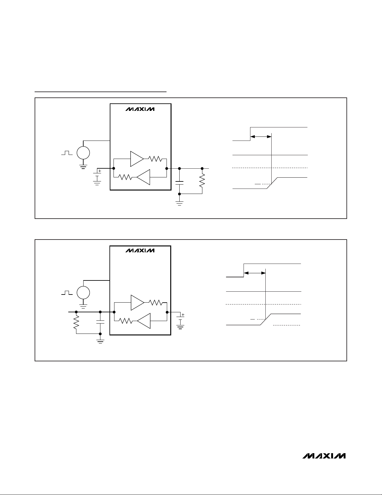
Test Circuits/Timing Diagrams
MAX13101E
MAX13102E
MAX13103E
MAX13108E
SOURCE
R
S
6kΩ
6kΩ
ALL UNUSED I/O V
CC_
AND I/O VL_ CONNECTED TO GND
I/O V
L_
EN/(MULT)
V
L
V
CC
I/O V
CC_
C
I/OVCC_
( ) ARE FOR THE MAX13108E
t
PHL
t
PLH
50%
90%
10%
I/O V
CC_
I/O V
L_
90%
50%
10%
90%
50%
10%
t
RISE/FALL
≤ 3ns
t
FVCC
t
PVL-VCC
= t
PHL
or t
PLH
t
RVCC
SOURCE
R
S
I/O V
L_
EN/(MULT)
V
L
V
CC
I/O V
CC_
C
I/OVL_
MAX13101E
MAX13102E
MAX13103E
MAX13108E
6kΩ
6kΩ
ALL UNUSED I/O V
CC_
AND I/O V
L_
CONNECTED TO GND
( ) ARE FOR THE MAX13108E
t
PHL
t
PLH
I/O V
L_
I/O V
CC_
90%
50%
10%
90%
50%
10%
50%
90%
10%
t
RISE/FALL
≤ 3ns
t
FVL
t
RVL
t
PVCC-VL
= t
PHL
or t
PLH
Figure 1a. Driving I/O V
L_
Figure 1b. Timing for Driving I/O V
L_
Figure 2a. Driving I/O V
CC_
Figure 2b. Timing for Driving I/O V
CC_
Page 6
MAX13101E/MAX13102E/MAX13103E/MAX13108E
16-Channel Buffered CMOS
Logic-Level Translators
6 _______________________________________________________________________________________
Test Circuits/Timing Diagrams (continued)
SOURCE
I/O V
CC_
100kΩ
I/O V
L_
C
I/OVCC
V
L
EN/(MULT)
I/O V
L_
I/O V
CC_
t
EN-VCC
V
L
V
L
V
CC
0
0
V
CC
2
MAX13101E
MAX13102E
MAX13103E
MAX13108E
EN/(MULT)
( ) ARE FOR THE MAX13108E
6kΩ
6kΩ
Figure 3. Propagation Delay from I/O VL_to I/O V
CC_
After EN
I/O V
CC_
I/O V
L_
C
I/OVL
100kΩ
V
CC
EN/(MULT)
I/O V
L_
I/O V
CC_
t
EN-VL
V
L
V
L
V
CC
0
0
0
V
L
2
SOURCE
MAX13101E
MAX13102E
MAX13103E
MAX13108E
EN/(MULT)
( ) ARE FOR THE MAX13108E
6kΩ
6kΩ
Figure 4. Propagation Delay from I/O V
CC_
to I/O VL_After EN
Page 7

MAX13101E/MAX13102E/MAX13103E/MAX13108E
16-Channel Buffered CMOS
Logic-Level Translators
_______________________________________________________________________________________ 7
VL SUPPLY CURRENT vs. V
CC
SUPPLY VOLTAGE
(DRIVING I/0 V
L_
, VL = 1.8V)
VCC SUPPLY VOLTAGE (V)
V
L
SUPPLY CURRENT (μA)
MAX13101-3/8E toc01
1.5 2.0 2.5 3.0 3.5 4.0 4.5 5.0 5.5
0
20
40
60
80
100
120
DRIVING ONE I/O VL
FIGURE 1a
C
I/OVCC_
= 15pF
VL SUPPLY CURRENT vs. VL SUPPLY VOLTAGE
(DRIVING I/0 V
CC_
, VCC = 5.5V)
VL SUPPLY VOLTAGE (V)
V
L
SUPPLY CURRENT (μA)
.
1.5 2.0 2.5 3.0 3.5 4.0 4.5 5.0 5.5
0
500
1000
1500
2000
2500
DRIVING ONE I/O V
CC
FIGURE 2a
C
I/OVL_
= 15pF
MAX13101-3/8E toc02
VCC SUPPLY CURRENT vs. VL SUPPLY VOLTAGE
(DRIVING I/0 V
CC_
, VCC = 5.5V)
VL SUPPLY VOLTAGE (V)
V
CC
SUPPLY CURRENT (μA)
MAX13101-3/8 toc04
1.5 2.0 2.5 3.0 3.5 4.0 4.5 5.0 5.5
0
1000
2000
3000
4000
5000
6000
7000
8000
DRIVING ONE I/O V
CC
FIGURE 2a
C
I/OVL_
= 15pF
VCC SUPPLY CURRENT vs. V
CC
SUPPLY VOLTAGE
(DRIVING I/0 V
L_
, VL = 1.8V)
VCC SUPPLY VOLTAGE (V)
V
CC
SUPPLY CURRENT (μA)
MAX13101-3/8 toc03
1.5 2.0 2.5 3.0 3.5 4.0 4.5 5.0 5.5
0
1000
2000
3000
4000
5000
6000
7000
8000
DRIVING ONE I/O V
L
FIGURE 1a
C
I/OVCC_
= 15pF
V
L
SUPPLY CURRENT vs. TEMPERATURE
(DRIVING I/O V
CC_
)
TEMPERATURE (°C)
V
L
SUPPLY CURRENT (μA)
MAX13101-3/8E toc05
-40 -15 10 35 60 85
0
100
200
300
400
500
600
700
800
DRIVING ONE I/O V
CC
FIGURE 2a
C
I/OVL_
= 15pF
VCC SUPPLY CURRENT vs. TEMPERATURE
(DRIVING I/O V
CC_
)
TEMPERATURE (°C)
V
CC
SUPPLY CURRENT (μA)
MAX13101-3/8 toc06
-40 -15 10 35 60 85
0
500
1000
1500
2000
2500
3000
DRIVING ONE I/O V
CC
FIGURE 2a
C
I/OVL_
= 15pF
Typical Operating Characteristics
(VCC= 3.3V, VL= 1.8V, data rate = 20Mbps, TA = +25°C, unless otherwise noted.)
Page 8

RISE/FALL TIME vs. CAPACITIVE LOAD
ON I/O V
L_
(DRIVING I/O V
CC_
)
CAPACITIVE LOAD (pF)
RISE/FALL TIME (ns)
MAX13101-3/8E toc10
10 20 30 40 50
0
1
2
3
4
5
6
7
t
FVL
t
RVL
FIGURES 2a, 2b
PROPAGATION DELAY vs. CAPACITIVE LOAD
ON I/O V
CC_
(DRIVING I/O VL_)
CAPACITIVE LOAD (pF)
PROPAGATION DELAY (ns)
MAX13101-3/8E toc11
10 20 30 40 50
0
2
4
6
8
10
t
PLH
t
PHL
FIGURES 1a, 1b
MAX13101E/MAX13102E/MAX13103E/MAX13108E
16-Channel Buffered CMOS
Logic-Level Translators
8 _______________________________________________________________________________________
V
L
SUPPLY CURRENT vs. CAPACITIVE LOAD
ON I/O V
L_
(DRIVING I/O V
CC_
)
CAPACITIVE LOAD (pF)
V
L
SUPPLY CURRENT (μA)
MAX13101-3/8E toc07
10 20 30 40 50
0
200
400
600
800
1000
1200
DRIVING ONE I/O V
CC
FIGURE 2a
VCC SUPPLY CURRENT vs. CAPACITIVE LOAD
ON I/O V
CC_
(DRIVING I/O VL_)
CAPACITIVE LOAD (pF)
V
CC
SUPPLY CURRENT (μA)
MAX13101-3/8E toc08
10 20 30 40 50
0
1000
2000
3000
4000
5000
DRIVING ONE I/O V
L
FIGURE 1a
RISE/FALL TIME vs. CAPACITIVE LOAD ON
I/O V
CC
_ (DRIVING I/O VL_)
CAPACITIVE LOAD (pF)
RISE/FALL TIME (ns)
MAX13101-3/8E toc09
10 20 30 40 50
0
1
2
3
4
t
RVCC
t
FVCC
FIGURES 1a, 1b
Typical Operating Characteristics (continued)
(VCC= 3.3V, VL= 1.8V, data rate = 20Mbps, TA = +25°C, unless otherwise noted.)
Page 9

MAX13101E/MAX13102E/MAX13103E/MAX13108E
Pin Description—MAX13101E/MAX13102E/MAX13103E
PIN
TQFN WLP
FUNCTION
1, 21, 30
D6 GND Ground
2 C2
Input/Output 5. Referenced to VL.
3 A3
Input/Output 6. Referenced to VL.
4 B3
Input/Output 7. Referenced to VL.
5 C3
Input/Output 8. Referenced to VL.
6 A4
Input/Output 9. Referenced to VL.
7 B4
Input/Output 10. Referenced to VL.
8 C4
Input/Output 11. Referenced to VL.
9 A5
Input/Output 12. Referenced to VL.
10 C6 EN Global Enable Input. Pull EN low for shutdown. Drive EN to V
CC
or VL for normal operation.
11 B5
Input/Output 13. Referenced to VL.
12 C5
Input/Output 14. Referenced to VL.
13 A6
Input/Output 15. Referenced to VL.
14 B6
Input/Output 16. Referenced to VL.
15, 36 A1 V
L
Logic Supply Voltage, +1.2V ≤ VL ≤ VCC. Bypass VL to GND with a 0.1µF capacitor.
16, 35 F1 V
CC
VCC Supply Voltage, +1.65V ≤ V
CC
≤ +5.5V. Bypass VCC to GND with a 0.1µF capacitor.
For full ESD protection, connect a 1.0µF capacitor from VCC to GND, located as close to the
VCC input as possible.
17 E6
Input/Output 16. Referenced to VCC.
18 F6
Input/Output 15. Referenced to VCC.
RAIL-TO-RAIL DRIVING (DRIVING I/O VL)
10ns/div
MAX13101E-3/8E toc13
I/0 V
L_
1V/div
I/0 V
CC_
2V/div
GND
GND
C
I/OVCC_
= 50pF
Typical Operating Characteristics (continued)
(VCC= 3.3V, VL= 1.8V, data rate = 20Mbps, TA = +25°C, unless otherwise noted.)
16-Channel Buffered CMOS
Logic-Level Translators
_______________________________________________________________________________________ 9
PROPAGATION DELAY vs. CAPACITIVE LOAD
ON I/O V
L_
(DRIVING I/O V
CC_
)
CAPACITIVE LOAD (pF)
PROPAGATION DELAY (ns)
MAX13101-3/8E toc12
10 20 30 40 50
0
1
2
3
4
5
t
PHL
t
PLH
FIGURES 2a, 2b
NAME
I/O VL5
I/O VL6
I/O VL7
I/O VL8
I/O VL9
I/O VL10
I/O VL11
I/O VL12
I/O VL13
I/O VL14
I/O VL15
I/O VL16
I/O VCC16
I/O VCC15
Page 10

MAX13101E/MAX13102E/MAX13103E/MAX13108E
16-Channel Buffered CMOS
Logic-Level Translators
10 ______________________________________________________________________________________
Pin Description—MAX13101E/MAX13102E/MAX13103E (continued)
PIN
TQFN WLP
NAME
FUNCTION
19 D5
Input/Output 14. Referenced to VCC.
20 E5
Input/Output 13. Referenced to VCC.
22 F5
Input/Output 12. Referenced to VCC.
23 D4
Input/Output 11. Referenced to VCC.
24 E4
Input/Output 10. Referenced to VCC.
25 F4
Input/Output 9. Referenced to VCC.
26 D3
Input/Output 8. Referenced to VCC.
27 E3
Input/Output 7. Referenced to VCC.
28 F3
Input/Output 6. Referenced to VCC.
29 D2
Input/Output 5. Referenced to VCC.
31 E2
Input/Output 4. Referenced to VCC.
32 F2
Input/Output 3. Referenced to VCC.
33 D1
Input/Output 2. Referenced to VCC.
34 E1
Input/Output 1. Referenced to VCC.
37 B1
Input/Output 1. Referenced to VL.
38 C1
Input/Output 2. Referenced to VL.
39 A2
Input/Output 3. Referenced to VL.
40 B2
Input/Output 4. Referenced to VL.
— — EP Exposed Pad. Connect EP to GND.
Pin Description—MAX13108E
PIN
TQFN WLP
FUNCTION
1, 21, 30
D6 GND Ground
2 C2
Input/Output 5. Referenced to VL.
3 A3
Input/Output 6. Referenced to VL.
4 B3
Input/Output 7. Referenced to VL.
5 C3
Input/Output 8. Referenced to VL.
6 A4
Input/Output 9. Referenced to VL.
7 B4
Input/Output 10. Referenced to VL.
8 C4
Input/Output 11. Referenced to VL.
9 A5
Input/Output 12. Referenced to VL.
I/O VCC14
I/O VCC13
I/O VCC12
I/O VCC11
I/O VCC10
I/O VCC9
I/O VCC8
I/O VCC7
I/O VCC6
I/O VCC5
I/O VCC4
I/O VCC3
I/O VCC2
I/O VCC1
I/O VL1
I/O VL2
I/O VL3
I/O VL4
NAME
I/O VL5
I/O VL6
I/O VL7
I/O VL8
I/O VL9
I/O VL10
I/O VL11
I/O VL12
Page 11

MAX13101E/MAX13102E/MAX13103E/MAX13108E
16-Channel Buffered CMOS
Logic-Level Translators
______________________________________________________________________________________ 11
Pin Description—MAX13108E (continued)
PIN
TQFN WLP
FUNCTION
10 C6 MULT
Multiplexing Input. Drive MULT low to enable channels 9 to 16. Driving MULT low puts
channels 1 to 8 into tri-state. Drive MULT to V
CC
or VL to enable channels 1 to 8. Driving
MULT to VCC or VL puts channels 9 to 16 into tri-state.
11 B5
Input/Output 13. Referenced to VL.
12 C5
Input/Output 14. Referenced to VL.
13 A6
Input/Output 15. Referenced to VL.
14 B6
Input/Output 16. Referenced to VL.
15, 36 A1 V
L
Logic Supply Voltage, +1.2V ≤ VL ≤ VCC. Bypass VL to GND with a 0.1µF capacitor.
16, 35 F1 V
CC
VCC Supply Voltage, +1.65V ≤ V
CC
≤ +5.5V. Bypass V
CC
to GND with a 0.1µF capacitor.
For full ESD protection, connect a 1.0µF capacitor from VCC to GND, located as close to the
VCC input as possible.
17 E6
Input/Output 16. Referenced to VCC.
18 F6
Input/Output 15. Referenced to VCC.
19 D5
Input/Output 14. Referenced to VCC.
20 E5
Input/Output 13. Referenced to VCC.
22 F5
Input/Output 12. Referenced to VCC.
23 D4
Input/Output 11. Referenced to VCC.
24 E4
Input/Output 10. Referenced to VCC.
25 F4
Input/Output 9. Referenced to VCC.
26 D3
Input/Output 8. Referenced to VCC.
27 E3
Input/Output 7. Referenced to VCC.
28 F3
Input/Output 6. Referenced to VCC.
29 D2
Input/Output 5. Referenced to VCC.
31 E2
Input/Output 4. Referenced to VCC.
32 F2
Input/Output 3. Referenced to VCC.
33 D1
Input/Output 2. Referenced to VCC.
34 E1
Input/Output 1. Referenced to VCC.
37 B1
Input/Output 1. Referenced to VL.
38 C1
Input/Output 2. Referenced to VL.
39 A2
Input/Output 3. Referenced to VL.
40 B2
Input/Output 4. Referenced to VL.
— — EP Exposed Pad. Connect EP to GND.
NAME
I/O VL13
I/O VL14
I/O VL15
I/O VL16
I/O VCC16
I/O VCC15
I/O VCC14
I/O VCC13
I/O VCC12
I/O VCC11
I/O VCC10
I/O VCC9
I/O VCC8
I/O VCC7
I/O VCC6
I/O VCC5
I/O VCC4
I/O VCC3
I/O VCC2
I/O VCC1
I/O VL1
I/O VL2
I/O VL3
I/O VL4
Page 12

MAX13101E/MAX13102E/MAX13103E/MAX13108E
16-Channel Buffered CMOS
Logic-Level Translators
12 ______________________________________________________________________________________
EN
V
CC
I/O V
L
1
I/O V
L
2
I/O V
L
3
I/O V
L
4
I/O V
L
5
I/O V
L
6
I/O V
L
7
I/O V
L
8
I/O V
L
9
I/O V
L
10
I/O V
L
11
I/O V
L
12
I/O V
L
13
I/O V
L
14
I/O V
L
15
I/O V
L
16
I/O V
CC
1
I/O V
CC
2
I/O V
CC
3
I/O V
CC
4
I/O V
CC
5
I/O V
CC
6
I/O V
CC
7
I/O V
CC
8
I/O V
CC
9
I/O V
CC
10
I/O V
CC
11
I/O V
CC
12
I/O V
CC
13
I/O V
CC
14
I/O V
CC
15
GND
I/O V
CC
16
V
L
MAX13101E
MAX13102E
MAX13103E
Functional Diagrams
MULT
I/O V
L
1
I/O V
L
2
I/O V
L
3
I/O V
L
4
I/O V
L
5
I/O V
L
6
I/O V
L
7
I/O V
L
8
I/O V
L
9
I/O V
L
10
I/O V
L
11
I/O V
L
12
I/O V
L
13
I/O V
L
14
I/O V
L
15
I/O V
L
16
I/O V
CC
1
I/O V
CC
2
I/O V
CC
3
I/O V
CC
4
I/O V
CC
5
I/O V
CC
6
I/O V
CC
7
I/O V
CC
8
I/O V
CC
9
I/O V
CC
10
I/O V
CC
11
I/O V
CC
12
I/O V
CC
13
I/O V
CC
14
I/O V
CC
15
I/O V
CC
16
GND
MAX13108E
V
L
V
CC
Page 13

MAX13101E/MAX13102E/MAX13103E/MAX13108E
16-Channel Buffered CMOS
Logic-Level Translators
______________________________________________________________________________________ 13
Detailed Description
The MAX13101E/MAX13102E/MAX13103E/MAX13108E
logic-level translators provide the level shifting necessary to allow data transfer in a multivoltage system.
Externally applied voltages, V
CC
and VL, set the logic
levels on either side of the device. Logic signals present on the V
L
side of the device appear as a higher
voltage logic signal on the V
CC
side of the device, and
vice-versa. The MAX13101E/MAX13102E/MAX13103E/
MAX13108E are bidirectional level translators allowing
data translation in either direction (VL↔VCC) on
any single data line. The MAX13101E/MAX13102E/
MAX13103E/MAX13108E accept V
L
from +1.2V to VCC.
All devices have a VCCrange from +1.65V to +5.5V,
making them ideal for data transfer between low-voltage ASICs/PLDs and higher voltage systems.
The MAX13101E/MAX13102E/MAX13103E feature an
output enable mode that reduces V
CC
supply current to
less than 1µA, and V
L
supply current to less than 2µA
when in shutdown. The MAX13108E features a multiplexing input that selects one byte between the two,
thus allowing multiplexing of the signals. The
MAX13101E/MAX13102E/MAX13103E/MAX13108E
have ±15kV ESD protection on the I/O VCCside for
greater protection in applications that route signals
externally. The MAX13101E/MAX13102E/MAX13103E/
MAX13108E operate at a guaranteed data rate of
20Mbps. The maximum data rate depends heavily
on the load capacitance (see the
Typical Operating
Characteristics
) and the output impedance of the
external driver.
Power-Supply Sequencing
For proper operation, ensure that +1.65V ≤ VCC≤ +5.5V,
+1.2V ≤ VL≤ +5.5V, and VL≤ VCC. During power-up
sequencing, VL≥ V
CC
does not damage the device.
When VCCis disconnected and VLis powering up, up to
10mA of current can be sourced to each load on the V
L
side, yet the device does not latch up. To guarantee that
no excess leakage current flows and that the device
does not interfere with the I/O on the VLside, VCCshould
be connected to GND with a max 50Ω resistor when the
VCCsupply is not present (Figure 5).
Input Driver Requirements
The MAX13101E/MAX13102E/MAX13103E/MAX13108E
architecture is based on a one-shot accelerator output
stage (Figure 6). Accelerator output stages are always
in tri-state except when there is a transition on any of
the translators on the input side, either I/O VL_ or
I/O VCC_. Then a short pulse is generated, during
which the accelerator output stages become active and
charge/discharge the capacitances at the I/Os. Due to
the bidirectional nature, both input stages become
active during the one-shot pulse. This can lead to some
current feeding into the external source that is driving
the translator. However, this behavior helps to speed
up the transition on the driven side.
For proper full-speed operation, the output current of a
device that drives the inputs of the MAX13101E/
MAX13102E/MAX13103E/MAX13108E should meet the
following requirement:
i > 10
8
x V x (C + 10pF)
where, i is the driver output current, V is the logic-supply
voltage (i.e., VLor VCC) and C is the parasitic capacitance of the signal line.
Enable Output Mode (EN)
The MAX13101E/MAX13102E/MAX13103E feature an
enable input (EN) that, when driven low, places the
device into shutdown mode. During shutdown, the
MAX13101E I/O VCC_ ports are pulled down to ground
with internal 6kΩ resistors and the I/O VL_ ports enter
tri-state. MAX13102E I/O VCC_ lines enter tri-state and
the I/OV
L
_ lines are pulled down to ground with internal
6kΩ resistors. All I/O VCC_ and I/O VL_ lines on the
MAX13103E enter tri-state while the device is in shutdown mode. During shutdown, the VCCsupply current
reduces to less than 1µA, and the VLsupply current
reduces to less than 2µA. To guarantee minimum shutdown supply current, all I/O VL_ need to be driven to
GND or VL, or pulled to GND or VLthrough 100kΩ
resistors. All I/O VCC_ need to be driven to GND or
V
CC,
or pulled to GND or V
CC
through 100kΩ resistors.
Drive EN to logic-high (VLor VCC) for normal operation.
I/O VCC16 I/O VL16
I/O V
L
1
I/O V
CC
1
V
CC
V
L
+1.2V TO +5.5V
GND
V
CC
SUPPLY
V
BATT
DISABLE
R
DSON
< 50Ω
MAX13101E
MAX13102E
MAX13103E
MAX13108E
Figure 5. Recommended Circuit for Powering Down V
CC
Page 14

MAX13101E/MAX13102E/MAX13103E/MAX13108E
16-Channel Buffered CMOS
Logic-Level Translators
14 ______________________________________________________________________________________
Multiplexing Input (MULT)
The MAX13108E features a multiplexing input (MULT)
that enables 8 of the 16 channels and places the
remaining 8 into tri-state. Figure 7 depicts a typical multiplexing configuration using the MAX13108E. Drive
MULT high to enable I/O VCC1 through I/O VCC8 and
I/O VL1 through I/O VL8. Driving MULT high sets
I/O VCC9 through I/O VCC16 and I/O VL9 through I/O
VL16 into tri-state. Drive MULT low to enable I/O VCC9
through I/O VCC16 and I/O VL9 through I/O VL16.
Driving MULT low sets I/O VCC1 through I/O VCC8 and
I/O VL1 through I/O VL8 into tri-state.
±15kV ESD Protection
As with all Maxim devices, ESD-protection structures are
incorporated on all pins to protect against electrostatic
discharges encountered during handling and assembly.
The I/O VCC_ lines have extra protection against static
discharge. Maxim’s engineers have developed state-ofthe-art structures to protect these pins against ESD of
±15kV without damage. The ESD structures withstand
high ESD in all states: normal operation, tri-state output
mode, and powered down. After an ESD event, Maxim’s
E versions keep working without latchup, whereas competing products can latch and must be powered down
to remove the latchup condition.
ESD protection can be tested in various ways. The
I/O VCC_ lines of the MAX13101E/ MAX13102E/
MAX13103E/MAX13108E are characterized for protection to ±15kV using the Human Body Model.
RISE-TIME
ACCELERATOR
FALL-TIME
ACCELERATOR
I/O V
CC_
I/O V
L_
V
CC
V
L
RISE-TIME
ACCELERATOR
FALL-TIME
ACCELERATOR
MAX13101E
MAX13102E
MAX13103E
MAX13108E
Figure 6. Simplified Diagram (1 I/O Line)
PORT A
PORT B
I/O V
L
9
I/O V
L
10
I/O V
L
11
I/O V
L
12
I/O V
L
13
I/O V
L
14
I/O V
L
15
I/O V
L
16
I/O V
L
3
I/O V
L
4
I/O V
L
5
I/O V
L
6
I/O V
L
7
I/O V
L
8
I/O V
L
1
I/O V
L
2
I/O VCC1
MULT
I/O V
CC
2
I/O V
CC
3
I/O V
CC
4
I/O V
CC
5
I/O V
CC
6
I/O V
CC
7
I/O V
CC
8
I/O V
CC
9
I/O V
CC
10
I/O V
CC
11
I/O V
CC
12
I/O V
CC
13
I/O V
CC
14
I/O V
CC
15
I/O V
CC
16
MAX13108E
Figure 7. MAX13108E Multiplexing Configuration
Page 15

MAX13101E/MAX13102E/MAX13103E/MAX13108E
16-Channel Buffered CMOS
Logic-Level Translators
______________________________________________________________________________________ 15
ESD Test Conditions
ESD performance depends on a variety of conditions.
Contact Maxim for a reliability report that documents
test setup, test methodology, and test results.
Human Body Model
Figure 8a shows the Human Body Model and Figure 8b
shows the current waveform it generates when discharged into a low impedance. This model consists of
a 100pF capacitor charged to the ESD voltage of interest, which is then discharged into the test device
through a 1.5kΩ resistor.
Machine Model
The Machine Model for ESD tests all pins using a
200pF storage capacitor and zero discharge resistance. Its objective is to emulate the stress caused by
contact that occurs with handling and assembly during
manufacturing. All pins require this protection during
manufacturing, not just inputs and outputs. Therefore,
after PC board assembly, the Machine Model is less
relevant to I/O ports.
Applications Information
Power-Supply Decoupling
To reduce ripple and the chance of transmitting incorrect data, bypass VLand VCCto ground with 0.1µF
capacitors. To ensure full ±15kV ESD protection,
bypass VCCto ground with a 1µF ceramic capacitor.
Place all capacitors as close to the power-supply inputs
as possible.
Capacitive Loading
Capacitive loading on the I/O lines impacts the rise time
(and fall time) of the MAX13101E/MAX13102E/
MAX13103E/MAX13108E when driving the signal lines.
The actual rise time is a function of the parasitic capacitance, the supply voltage, and the drive impedance of
the MAX13101E/MAX13102E/MAX13103E/MAX13108E.
For proper operation, the signal must reach the VOHas
required before the rise-time accelerators turn off.
HIGH-
VOLTAGE
DC
SOURCE
DEVICE
UNDER
TEST
R
C
1MΩ RD 1500Ω
CHARGE-CURRENT-
LIMIT RESISTOR
DISCHARGE
RESISTANCE
STORAGE
CAPACITOR
C
S
100pF
Figure 8a. Human Body ESD Test Model
100%
90%
36.8%
t
RL
t
DL
TIME
CURRENT WAVEFORM
PEAK-TO-PEAK RINGING
(NOT DRAWN TO SCALE)
10%
0
0
AMPERES
I
P
I
r
Figure 8b. Human Body Model Current Waveform
Page 16

MAX13101E/MAX13102E/MAX13103E/MAX13108E
16-Channel Buffered CMOS
Logic-Level Translators
16 ______________________________________________________________________________________
Ordering Information/Selector Guide (continued)
PART PIN-PACKAGE
DATA
I/O VL STATE
I/O VCC STATE
MULTIPLEXER
FEATURE
MAX13102EEWX+
36 WLP**
3.06mm x 3.06mm
20 6kΩ to GND High impedance No
MAX13102EETL+
40 TQFN-EP***
20 6kΩ to GND High impedance No
MAX13103EEWX+
36 WLP**
3.06mm x 3.06mm
20 High impedance High impedance No
MAX13103EETL+
40 TQFN-EP***
20 High impedance High impedance No
MAX13108EEWX+
36 WLP**
3.06mm x 3.06mm
20 High impedance High impedance Yes
MAX13108EETL+
40 TQFN-EP***
20 High impedance High impedance Yes
Pin Configurations (continued)
MA131018E
TQFN
+
TOP VIEW OF BOTTOM LEADS
56
4
3
I/O V
L
14
I/O V
L
16
V
L
V
CC
I/O V
CC
16
I/O V
L
13
I/O V
L
3
I/O V
L
1
V
L
I/O VL4
V
CC
I/O V
CC
1
11
12
I/O V
L
7
14
15
16
17
I/O V
L
8
I/O V
L
9
I/O V
CC
7
I/O V
CC
8
I/O V
CC
9
I/O V
CC
10
I/O VL15
I/O V
L
2
13
7
I/O V
L
10
I/O V
CC
11
8
* EXPOSED PAD CONNECTED TO GROUND
I/O V
L
11
I/O V
L
12
MULT
I/O V
CC
12
GND
9 10
I/O V
L
6
2
I/O V
CC
6
I/O V
L
5
1
I/O V
CC
5
GND
26 25
27
28 24 23 22 212930
I/O V
CC
15
I/O V
CC
14
I/O V
CC
13
I/O V
CC
2
I/O V
CC
3
I/O V
CC
4
18
19
20
40
39
37
36
35
34
38
33
32
31
GND
*EP
Note:
All devices are specified over the -40°C to +85°C operating temperature range.
+
Denotes a lead-free/RoHS-compliant package.
**
WLP bumps are in a 6 x 6 array.
***
EP = Exposed pad.
RATE (Mbps)
DURING SHUTDOWN
5mm x 5mm x 0.8mm
5mm x 5mm x 0.8mm
5mm x 5mm x 0.8mm
DURING SHUTDOWN
Page 17

MAX13101E/MAX13102E/MAX13103E/MAX13108E
16-Channel Buffered CMOS
Logic-Level Translators
______________________________________________________________________________________ 17
Pin Configurations (continued)
123456
E
D
F
WLP
(BOTTOM VIEW)
WLP
(BOTTOM VIEW)
I/O V
CC
3 I/O VCC6 I/O VCC9 I/O VCC12 I/O VCC15
I/O V
CC
1 I/O VCC4 I/O VCC7 I/O VCC10 I/O VCC13 I/O VCC16
I/O VCC2 I/O VCC5 I/O VCC8 I/O VCC11 I/O VCC14 GND
I/O VL2 I/O VL5 I/O VL8 I/O VL11 I/O VL14 EN
I/O VL1 I/O VL4 I/O VL7 I/O VL10 I/O VL13 I/O VL16
V
L
I/O VL3 I/O VL6 I/O VL9 I/O VL12 I/O VL15
B
A
C
MAX13101E/MAX13102E/MAX13103E
123456
E
D
F
V
CC
V
CC
I/O V
CC
3 I/O V
CC
6 I/O VCC9 I/O VCC12 I/O VCC15
I/O VCC1 I/O VCC4 I/O VCC7 I/O VCC10 I/O VCC13 I/O VCC16
I/O VCC2 I/O VCC5 I/O VCC8 I/O VCC11 I/O VCC14 GND
I/O VL2 I/O VL5 I/O VL8 I/O VL11 I/O VL14 MULT
I/O VL1 I/O VL4 I/O VL7 I/O VL10 I/O VL13 I/O VL16
V
L
I/O VL3 I/O VL6 I/O VL9 I/O VL12 I/O VL15
B
A
C
MAX13108E
++
Chip Information
PROCESS: BiCMOS
Typical Operating Circuit
MAX13101E
MAX13102E
MAX13103E
MAX13108E
+1.8V
+3.3V
+1.8V
SYSTEM
CONTROLLER
+3.3V
SYSTEM
DATA
( ) ARE FOR MAX13108E
DATA
GND
V
L
V
CC
I/O V
CC_
I/O V
L_
EN/(MULT)
Package Information
For the latest package outline information and land patterns, go
to www.maxim-ic.com/packages
.
PACKAGE TYPE PACKAGE CODE DOCUMENT NO.
36 WLP W363A3-1
21-0024
40 TQFN-EP T4055-1
21-0140
Page 18

MAX13101E/MAX13102E/MAX13103E/MAX13108E
16-Channel Buffered CMOS
Logic-Level Translators
Maxim cannot assume responsibility for use of any circuitry other than circuitry entirely embodied in a Maxim product. No circuit patent licenses are
implied. Maxim reserves the right to change the circuitry and specifications without notice at any time.
18
____________________Maxim Integrated Products, 120 San Gabriel Drive, Sunnyvale, CA 94086 408-737-7600
© 2008 Maxim Integrated Products is a registered trademark of Maxim Integrated Products, Inc.
Revision History
REVISION
NUMBER
DATE
DESCRIPTION
PAGES
CHANGED
2 8/06 Release of the MAX13101EETL+ —
3 6/08 Changed UCSP to WLP packaging
1, 2, 9, 10, 11, 16,
17, 18, 19
REVISION
 Loading...