

Page 1
19-6016; Rev 0; 10/11
+5.0V, ±15kV ESD-Protected, Fail-Safe,
Hot-Swap, RS-485/RS-422 Transceiver
General Description
The MAX13085E +5.0V, ±15kV ESD-protected, RS-485/
RS-422 transceiver features one driver and one receiver.
The device includes fail-safe circuitry, guaranteeing
a logic-high receiver output when receiver inputs are
open or shorted. The receiver outputs a logic-high if all
transmitters on a terminated bus are disabled (high
impedance). The MAX13085E includes a hot-swap
capability to eliminate false transitions on the bus during
power-up or hot insertion.
The MAX13085E features reduced slew-rate drivers
that minimize EMI and reduce reflections caused by
improperly terminated cables, allowing error-free data
transmission up to 500kbps.
The MAX13085E is ideal for half-duplex communications
and it draws 1.2mA of supply current when unloaded
or when fully loaded with the drivers disabled. The
MAX13085E has a 1/8-unit load receiver input impedance, allowing up to 256 transceivers on the bus.
The MAX13085E is available in an 8-pin SO and PDIP
packages.
MAX13085E
Features
S +5.0V Operation
S Extended ESD Protection for RS-485/RS-422 I/O
Pins ±15kV Human Body Model
S True Fail-Safe Receiver While Maintaining
EIA/TIA-485 Compatibility
S Hot-Swap Input Structures on DE and RE
S Enhanced Slew-Rate Limiting Facilitates Error-
Free Data Transmission
S Low-Current Shutdown Mode
S Allow Up to 256 Transceivers on the Bus
S Available in Industry-Standard 8-Pin SO and PDIP
Packages
Applications
Utility Meters
Lighting Systems
Industrial Control
Ordering Information
PART TEMP RANGE PIN-PACKAGE
MAX13085EESA+
+Denotes a lead(Pb)-free/RoHS-compliant package.
-40NC to +85NC
8 SO
Telecom
Security Systems
Instrumentation
Profibus
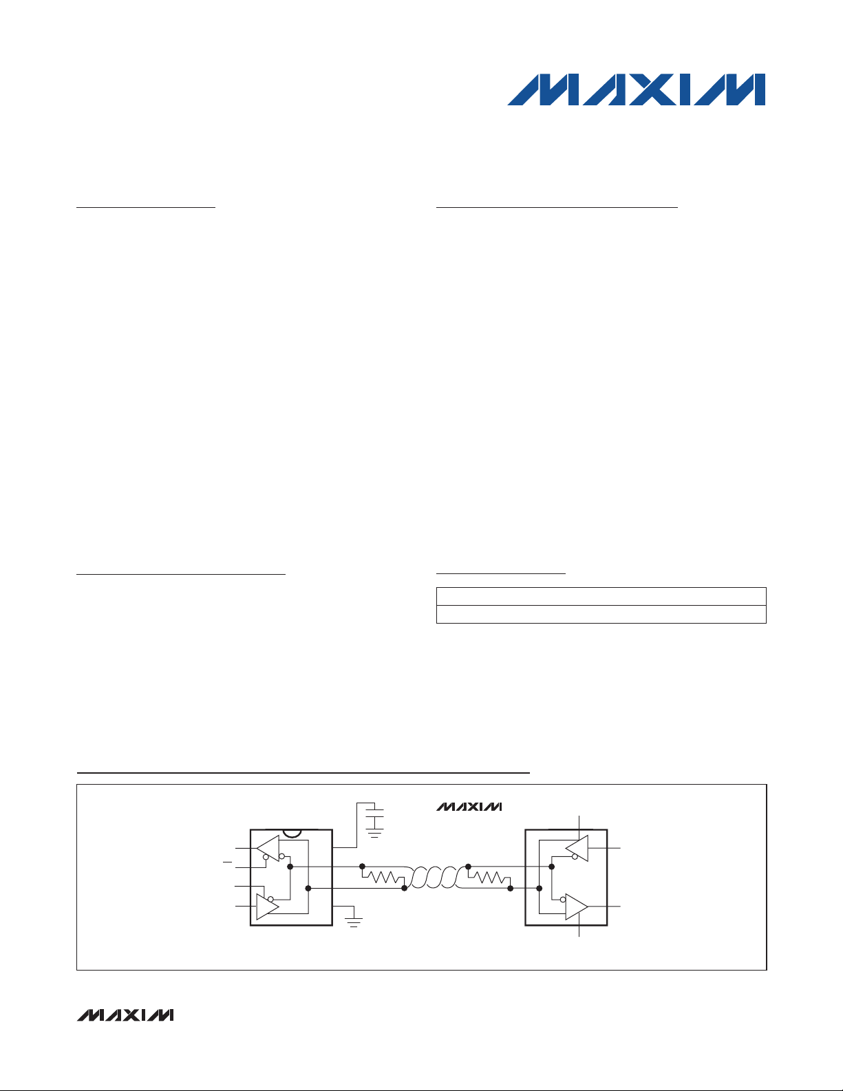
Typical Operating Circuit
0.1µF
+
1
RO
RE
DE
DI
R
2
3
4
D
8
V
CC
B
7
6
5
TYPICAL HALF-DUPLEX OPERATING CIRCUIT
Rt
A
GND
MAX13085E
DE
DI
B
Rt
A
D
RO
R
RE
_______________________________________________________________ Maxim Integrated Products 1
For pricing, delivery, and ordering information, please contact Maxim Direct at 1-888-629-4642,
or visit Maxim’s website at www.maxim-ic.com.
Page 2
+5.0V, ±15kV ESD-Protected, Fail-Safe,
Hot-Swap, RS-485/RS-422 Transceiver
ABSOLUTE MAXIMUM RATINGS
(All voltages referenced to GND.)
Supply Voltage (VCC) ........................................................... +6V
Control Input Voltage (RE, DE) ...............................-0.3V to +6V
Driver Input Voltage (DI) .........................................-0.3V to +6V
Driver Output Voltage (A, B) ....................................-8V to +13V
Receiver Input Voltage (A, B) ..................................-8V to +13V
Receiver Output Voltage (RO) ................. -0.3V to (VCC + 0.3V)
Driver Output Current .................................................... ±250mA
Stresses beyond those listed under “Absolute Maximum Ratings” may cause permanent damage to the device. These are stress ratings only, and functional
operation of the device at these or any other conditions beyond those indicated in the operational sections of the specifications is not implied. Exposure to absolute
MAX13085E
maximum rating conditions for extended periods may affect device reliability.
DC ELECTRICAL CHARACTERISTICS
(VCC = +5.0V ±10%, TA = T
PARAMETER SYMBOL CONDITIONS MIN TYP MAX UNITS
DRIVER
VCC Supply-Voltage Range V
Differential Driver Output V
Change in Magnitude of
Differential Output Voltage
Driver Common-Mode Output
Voltage
Change in Magnitude of
Common-Mode Voltage
Input-High Voltage V
Input-Low Voltage V
Input Hysteresis V
Input Current I
Input Impedance First Transition
at Power-Up
Input Impedance on First
Transition after POR Delay
Driver Short-Circuit Output
Current
Driver Short-Circuit Foldback
Output Current
Thermal-Shutdown Threshold T
Thermal-Shutdown Hysteresis T
Input Current (A and B) I
RECEIVER
Receiver Differential Threshold
Voltage
Receiver Input Hysteresis
MIN
to T
, unless otherwise noted. Typical values are at VCC = +5.0V and TA = +25NC.) (Note 1)
MAX
CC
RL = 100I (RS-422), Figure 1
RL = 54I (RS-485), Figure 1
No load V
RL = 100I or 54I, Figure 1 (Note 2)
OD
RL = 100I or 54I, Figure 1
RL = 100I or 54I, Figure 1 (Note 2)
OC
DE, DI, RE
IH
DE, DI, RE
IL
DE, DI, RE
DE, DI, RE
VDE, VRE = VRE = 2V
VDE = VRE = 2V
ft
0 P V
-7V P V
(VCC - 1V) P V
-7V P V
VDE = 0V,
VCC = 0V or V
-7V P VCM P +12V
VA + VB = 0V 15 mV
TH
P +12V (Note 3)
OUT
P VCC (Note 3)
OUT
P +1V (Note 3)
OUT
DV
V
DV
R
PWUP
I
OSD
I
OSDF
A, B
V
DV
OD
OC
HYS
IN1
R
TS
TSH
TH
Continuous Power Dissipation (TA = +70°C)
SO (derate 5.9mW/°C above +70°C) ..........................471mW
Operating Temperature Range .......................... -40°C to +85°C
Junction Temperature .....................................................+150°C
Storage Temperature Range ............................ -65°C to +150°C
Lead Temperature (soldering, 10s) ................................+300°C
Soldering Temperature (reflow) ......................................+260°C
4.5 5.5 V
P +12V (Note 3)
OUT
VIN = +12V 125
CC
VIN = -7V -100
3 V
2 V
VCC/2 3 V
3 V
100 mV
3.65 8.8
7 60 kΩ
40 250
-250 -40
20
175
15
-200 -125 -50 mV
CC
CC
CC
0.2 V
0.2 V
0.8 V
Q1 FA
-20
V
kI
mA
mA
NC
NC
FA
2 ______________________________________________________________________________________
Page 3
+5.0V, ±15kV ESD-Protected, Fail-Safe,
Hot-Swap, RS-485/RS-422 Transceiver
DC ELECTRICAL CHARACTERISTICS (continued)
(VCC = +5.0V ±10%, TA = T
PARAMETER SYMBOL CONDITIONS MIN TYP MAX UNITS
RO Output-High Voltage V
RO Output-Low Voltage V
Three-State Output Current at
Receiver
Receiver Input Resistance R
Receiver Output Short-Circuit
Current
SUPPLY CURRENT
Supply Current I
Supply Current in Shutdown
Mode
ESD PROTECTION
ESD Protection for A and B
MIN
to T
, unless otherwise noted. Typical values are at VCC = +5.0V and TA = +25NC.) (Note 1)
MAX
OH
OL
I
OZR
I
OSR
CC
I
SHDN
IO = -1mA
IO = 1mA 0.4 V
0 P VO P VCC P 1 FA
-7V P VCM P +12V
IN
0V P VRO P V
No load, VRE = 0V, DE = V
No load, RE = VCC, DE = V
No load, VRE = 0V, VDE = 0V
RE = VCC, VDE = 0V
Human Body Model
Contact Discharge
IEC 61000-4-2, level 4
Air-Gap Discharge
IEC 61000-4-2
CC
CC
CC
VCC -
0.6
96
P 110
1.2 1.8
1.2 1.8
1.2 1.8
2.8 10
Q15
Q8
Q15
MAX13085E
V
kI
mA
mA
FA
kV
DRIVER SWITCHING CHARACTERISTICS WITH INTERNAL SRL (500kbps)
(VCC = +5.0V ±10%, TA = T
PARAMETER SYMBOL CONDITIONS MIN TYP MAX UNITS
Driver Propagation Delay
Driver Differential Output Rise or
Fall Time
Differential Driver Output Skew
|t
- t
DPHL
|
_______________________________________________________________________________________ 3
DPLH
Maximum Data Rate 500 kbps
Driver Enable to Output High t
Driver Enable to Output Low t
Driver Disable Time from Low t
Driver Disable Time from High t
Driver Enable from Shutdown to
Output High
Driver Enable from Shutdown to
Output Low
Time to Shutdown t
MIN
to T
, unless otherwise noted. Typical values are at VCC = +5.0V and TA = +25NC.) (Note 1)
MAX
t
DPLH
t
DPHL
t
R , tF
t
DSKEW
DZH
DZL
DLZ
DHZ
t
DZH(SHDN)
t
DZL(SHDN)
SHDN
CL = 50pF, RL = 54I, Figures 2 and 3
CL = 50pF, RL = 54I, Figures 2 and 3
CL = 50pF, RL = 54I, Figures 2 and 3
Figure 4 2500 ns
Figure 5 2500 ns
Figure 5 100 ns
Figure 4 100 ns
Figure 4 5500 ns
Figure 5 5500 ns
200 1000
200 1000
250 900 ns
140 ns
50 340 700 ns
ns
Page 4
+5.0V, ±15kV ESD-Protected, Fail-Safe,
Hot-Swap, RS-485/RS-422 Transceiver
RECEIVER SWITCHING CHARACTERISTICS WITH INTERNAL SRL (500kbps)
(VCC = +5.0V ±10%, TA = T
PARAMETER SYMBOL CONDITIONS MIN TYP MAX UNITS
Receiver Propagation Delay
Receiver Output Skew
|t
- t
RPLH
RPHL
|
Maximum Data Rate 500 kbps
Receiver Enable to Output Low t
MAX13085E
Receiver Enable to Output High t
Receiver Disable Time from Low t
Receiver Disable Time from High t
Receiver Enable from Shutdown
to Output High
Receiver Enable from Shutdown
to Output Low
Time to Shutdown t
Note 1: All currents into the device are positive. All currents out of the device are negative. All voltages are referred to device
ground, unless otherwise noted.
Note 2: ΔVOD and ΔVOC are the changes in VOD and VOC, respectively, when the DI input changes state.
Note 3: The short-circuit output current applies to peak current just prior to foldback current limiting. The short-circuit foldback
output current applies during current limiting to allow a recovery from bus contention.
MIN
to T
, unless otherwise noted. Typical values are at VCC = +5.0V and TA = +25NC.) (Note 1)
MAX
t
RPLH
t
RPHL
t
RSKEW
RZL
RZH
RLZ
RHZ
t
RZH(SHDN)
t
RZL(SHDN)
SHDN
CL = 15pF, Figures 6 and 7
CL = 15pF, Figures 6 and 7 30 ns
Figure 8 50 ns
Figure 8 50 ns
Figure 8 50 ns
Figure 8 50 ns
Figure 8 5500 ns
Figure 8 5500 ns
50 340 700 ns
200
200
ns
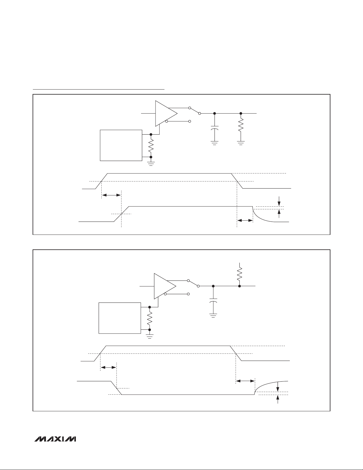
Test Circuits and Waveforms
B
RL/2
V
OD
R
L
A
Figure 1. Driver DC Test Load
V
CC
DE
DI
B
V
A
Figure 2. Driver Timing Test Circuit
V
/2
OC
R
OD
L C
L
V
CC
DI
VCC/2
0
Z
V
O
Y
1/2 V
O
V
O
V
DIFF
0
10%
-V
O
t
R
t
SKEW
t
90%
DPLH
= |
V
= V (B) - V (A)
DIFF
t
DPLH
-
Figure 3. Driver Propagation Delays
t
DPHL
t
DPHL
|
1/2 V
O
90%
t
F
10%
4 ______________________________________________________________________________________
Page 5
+5.0V, ±15kV ESD-Protected, Fail-Safe,
Hot-Swap, RS-485/RS-422 Transceiver
Test Circuits and Waveforms (continued)
S1
0 OR V
CC
D
C
L
50pF
R
= 500Ω
L
OUT
MAX13085E
GENERATOR
DE
t
, t
DZH
DZH(SHDN)
OUT
Figure 4. Driver Enable and Disable Times (t
0 OR V
VOM = (0 + VOH)/2
, t
DHZ
DZH
CC
50Ω
, t
DZH(SHDN)
D
V
CC
VCC/2
0
0.25V
t
DHZ
V
OH
0
)
V
CC
R
= 500Ω
S1
C
L
50pF
L
OUT
GENERATOR
DE
t
, t
DZL
DZL(SHDN)
V
CC
OUT
V
OL
Figure 5. Driver Enable and Disable Times (t
_______________________________________________________________________________________ 5
50Ω
VOM = (VOL + VCC)/2
, t
DZL
DLZ, tDLZ(SHDN)
V
CC
VCC/2
0
t
DLZ
0.25V
)
Page 6
+5.0V, ±15kV ESD-Protected, Fail-Safe,
Hot-Swap, RS-485/RS-422 Transceiver
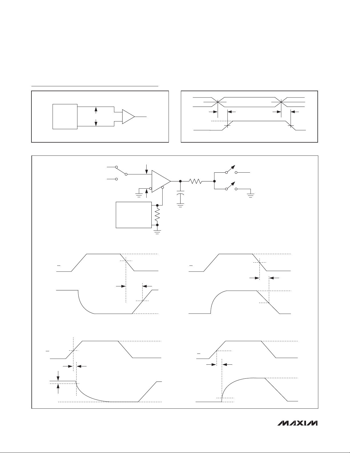
Test Circuits and Waveforms (continued)
A
RECEIVER
B
ATE
Figure 6. Receiver Propagation Delay Test Circuit Figure 7. Receiver Propagation Delays
MAX13085E
RE
RO
V
ID
+1.5V
-1.5V
S1 OPEN
S2 CLOSED
= +1.5V
V
S3
R
A
S3
GENERATOR
t
RZH
OUTPUT
, t
RZH(SHDN)
V
ID
VOH / 2
50Ω
V
0
V
0
CC
OH
B
t
V
OH
VCC/2
V
RO
C
15pF
OL
THE RISE TIME AND FALL TIME OF INPUTS A AND B < 4ns
1kΩ
L
RE
RO
RPLH
S1
S2
S1 CLOSED
S2 OPEN
= -1.5V
V
S3
t
RZL
V
CC
, t
RZL(SHDN)
VCC/2
(VOL + VCC)/2
+1V
-1V
t
RPHL
V
CC
0
V
CC
V
OL
S1 OPEN
S2 CLOSED
= +1.5V
V
S3
/250% 50%
V
RE
0.25V
RO
CC
t
RHZ
10%
V
CC
0
V
OH
0
RE
t
RLZ
10%
RO
S1 CLOSED
S2 OPEN
V
= -1.5V
S3
V
/2
CC
0.25V
Figure 8. Receiver Enable and Disable Times
6 ______________________________________________________________________________________
V
CC
0
V
CC
V
OL
Page 7

+5.0V, ±15kV ESD-Protected, Fail-Safe,
01
12345
345
45
Hot-Swap, RS-485/RS-422 Transceiver
Typical Operating Characteristics
(VCC = +5.0V, TA = +25°C, unless otherwise noted.)
MAX13085E
SUPPLY CURRENT vs. TEMPERATURE
1.60
1.50
1.40
1.30
1.20
1.10
SUPPLY CURRENT (mA)
1.00
0.90
0.80
-40 -10 520-25 35 50 9580 11065 125
TEMPERATURE (°C)
RECEIVER OUTPUT-HIGH VOLTAGE
vs. TEMPERATURE
5.4
5.2
5.0
4.8
4.6
4.4
OUTPUT HIGH VOLTAGE (V)
4.2
4.0
-40 -10 520-25 35 50 9580 11065 125
TEMPERATURE (°C)
NO LOAD
DE = V
DE = 0
IO = -1mA
OUTPUT CURRENT
vs. RECEIVER OUTPUT-HIGH VOLTAGE
60
50
MAX13085E toc01
40
CC
30
20
OUTPUT CURRENT (mA)
10
0
0213
OUTPUT HIGH VOLTAGE (V)
MAX13085E toc02
RECEIVER OUTPUT-LOW VOLTAGE
vs. RECEIVER OUTPUT-LOW VOLTAGE
70
60
50
40
30
OUTPUT CURRENT (mA)
20
10
0
021
DRIVER DIFFERENTIAL OUTPUT CURRENT
vs. TEMPERATURE
0.8
0.7
MAX13085E toc04
0.6
0.5
0.4
0.3
OUTPUT LOW VOLTAGE (V)
0.2
0.1
0
-40 -10 520-25 35 50 9580 11065 125
IO = 1mA
TEMPERATURE (°C)
160
140
MAX13085E toc05
120
100
80
60
40
DIFFERENTIAL OUTPUT CURRENT (mA)
20
0
0
OUTPUT CURRENT
MAX13085E toc03
OUTPUT LOW VOLTAGE (V)
vs. DIFFERENTIAL OUTPUT VOLTAGE
MAX13085E toc06
DIFFERENTIAL OUTPUT VOLTAGE (V)
DRIVER DIFFERENTIAL OUTPUT
VOLTAGE vs. TEMPERATURE
4.8
4.4
4.0
3.6
3.2
2.8
DIFFERENTIAL OUTPUT VOLTAGE (V)
2.4
2.0
-40 -10 520-25 35 50 9580 11065 125
TEMPERATURE (°C)
_______________________________________________________________________________________ 7
RL = 54Ω
200
180
MAX13085E toc07
160
140
120
100
80
60
OUTPUT CURRENT (mA)
40
20
0
-7 -5 -4-6 -3 -2 -1 0 123 54
OUTPUT CURRENT vs. TRANSMITTER
OUTPUT-HIGH VOLTAGE
OUTPUT HIGH VOLTAGE (V)
200
180
160
MAX13085E toc08
140
120
100
80
60
OUTPUT CURRENT (mA)
40
20
0
042681
OUTPUT CURRENT vs. TRANSMITTER
OUTPUT-LOW VOLTAGE
MAX13085E toc09
2
OUTPUT-LOW VOLTAGE (V)
Page 8

+5.0V, ±15kV ESD-Protected, Fail-Safe,
Hot-Swap, RS-485/RS-422 Transceiver
Typical Operating Characteristics (continued)
(VCC = +5.0V, TA = +25°C, unless otherwise noted.)
SHUTDOWN CURRENT
vs. TEMPERATURE
10
9
8
7
MAX13085E
6
5
4
3
SHUTDOWN CURRENT (µA)
2
1
0
-40 -10 520-25 35 50 9580 11065 125
TEMPERATURE (°C)
RECEIVER PROPAGATION DELAY
(500kbps)
DRIVER PROPAGATION DELAY
vs. TEMPERATURE (500kbps)
600
550
MAX13085E toc10
500
450
400
DRIVER PROPAGATION DELAY (ns)
350
300
-40 -10 520-25 35 50 9580 11065 125
MAX13085E toc13
RL = 100
VA - V
B
5V/div
RO
2V/div
TEMPERATURE (°C)
RECEIVER PROPAGATION DELAY
vs. TEMPERATURE (500kbps)
180
160
MAX13085E toc11
t
DPHL
t
DPLH
DRIVER PROPAGATION DELAY (500kbps)
140
120
100
80
60
40
RECEIVER PROPAGATION DELAY (ns)
20
0
-40 -10 520-25 35 50 9580 11065 125
MAX14780E toc14
RL = 100
TEMPERATURE (°C)
DI
2V/div
VY - V
Z
5V/div
t
DPLH
t
DPHL
MAX13085E toc12
200ns/div
400ns/div
8 ______________________________________________________________________________________
Page 9

+5.0V, ±15kV ESD-Protected, Fail-Safe,
Hot-Swap, RS-485/RS-422 Transceiver
Pin Configuration
+
RO
1
R
RE
2
DE
3
DI
D
4
SO
Pin Description
PIN NAME FUNCTION
1 RO
2
3 DE
4 DI
5 GND Ground
6 A Noninverting Receiver Input and Noninverting Driver Output
7 B Inverting Receiver Input and Inverting Driver Output
8 V
RE
CC
Receiver Output. When RE is low and if (A - B) R -50mV, RO is high; if (A - B) P -200mV, RO is low.
Receiver Output Enable. Drive RE low to enable RO; RO is high impedance when RE is high. Drive
RE high and DE low to enter low-power shutdown mode. RE is a hot-swap input (see the Hot-Swap
Capability section for details).
Driver Output Enable. Drive DE high to enable driver outputs. These outputs are high impedance
when DE is low. Drive RE high and DE low to enter low-power shutdown mode. DE is a hot-swap
input (see the Hot-Swap Capability section for details).
Driver Input. With DE high, a low on DI forces noninverting output low and inverting output high.
Similarly, a high on DI forces noninverting output high and inverting output low.
Positive Supply V
= +5.0V Q10%. Bypass VCC to GND with a 0.1FF capacitor.
CC
V
8
CC
B
7
6
A
5
GND
MAX13085E
Function Tables
TRANSMITTING
INPUTS OUTPUTS
RE
X 1 1 0 1
X 1 0 1 0
0 0 X High-Z High-Z
1 0 X Shutdown
DE DI B A
_______________________________________________________________________________________ 9
RE
0 X
0 X
0 X Open/shorted 1
1 1 X High-Z
1 0 X Shutdown
RECEIVING
INPUTS OUTPUTS
DE A-B RO
R -50mV
P -200mV
1
0
Page 10

+5.0V, ±15kV ESD-Protected, Fail-Safe,
Hot-Swap, RS-485/RS-422 Transceiver
Detailed Description
The MAX13085E high-speed transceiver for RS-485/
RS-422 communication contains one driver and one
receiver. This device features fail-safe circuitry, which
guarantees a logic-high receiver output when the receiver inputs are open or shorted, or when they are connected to a terminated transmission line with all drivers
disabled (see the Fail-Safe section). The MAX13085E
also features a hot-swap capability allowing line insertion without erroneous data transfer (see the Hot-Swap
MAX13085E
Capability section). The MAX13085E features reduced
slew-rate drivers that minimize EMI and reduce reflections caused by improperly terminated cables, allowing
error-free data transmission up to 500kbps.
The MAX13085E is a half-duplex transceiver and operates from a single +5.0V supply. Drivers are output
short-circuit current limited. Thermal-shutdown circuitry
protects drivers against excessive power dissipation.
When activated, the thermal-shutdown circuitry places
the driver outputs into a high-impedance state.
Fail-Safe
The MAX13085E guarantees a logic-high receiver output
when the receiver inputs are shorted or open, or when
they are connected to a terminated transmission line with
all drivers disabled. This is done by setting the receiver
input threshold between -50mV and -200mV. If the differential receiver input voltage (A - B) is greater than or
equal to -50mV, RO is logic-high. If (A - B) is less than
or equal to -200mV, RO is logic-low. In the case of a terminated bus with all transmitters disabled, the receiver’s
differential input voltage is pulled to 0V by the termination. With the receiver threshold of the MAX13085E,
this results in a logic-high with a 50mV minimum noise
margin. Unlike previous fail-safe devices, the -50mV to
-200mV threshold complies with the ±200mV EIA/TIA485 standard.
Additionally, parasitic circuit board capacitance could
cause coupling of VCC or GND to the enable inputs.
Without the hot-swap capability, these factors could
improperly enable the transceiver’s driver or receiver.
When VCC rises, an internal pulldown circuit holds DE
low and RE high. After the initial power-up sequence,
the pulldown circuit becomes transparent, resetting the
hot-swap tolerable input.
Hot-Swap Input Circuitry
The enable inputs feature hot-swap capability. At the
input there are two nMOS devices, M1 and M2 (Figure 9).
When VCC ramps from zero, an internal 7μs timer turns
on M2 and sets the SR latch, which also turns on M1.
Transistors M2, a 500μA current sink, and M1, a 100μA
current sink, pull DE to GND through a 5kΩ resistor.
M2 is designed to pull DE to the disabled state against
an external parasitic capacitance up to 100pF that can
drive DE high. After 7μs, the timer deactivates M2 while
M1 remains on, holding DE low against three-state leakages that can drive DE high. M1 remains on until an
external source overcomes the required input current.
At this time, the SR latch resets and M1 turns off. When
M1 turns off, DE reverts to a standard, high-impedance
V
CC
10µs
TIMER
SR LATCH
TIMER
Hot-Swap Capability
Hot-Swap Inputs
When circuit boards are inserted into a hot or powered
backplane, differential disturbances to the data bus
DE
5kΩ
can lead to data errors. Upon initial circuit board insertion, the data communication processor undergoes
its own power-up sequence. During this period, the
processor’s logic-output drivers are high impedance
100µA
500µA
M2M1
and are unable to drive the DE and RE inputs of these
devices to a defined logic level. Leakage currents up
to ±10μA from the high-impedance state of the processor’s logic drivers could cause standard CMOS enable
inputs of a transceiver to drift to an incorrect logic level.
10 _____________________________________________________________________________________
Figure 9. Simplified Structure of the Driver Enable Pin (DE)
DE
(HOT SWAP)
Page 11

+5.0V, ±15kV ESD-Protected, Fail-Safe,
Hot-Swap, RS-485/RS-422 Transceiver
CMOS input. Whenever VCC drops below 1V, the hotswap input is reset.
For RE there is a complementary circuit employing two
pMOS devices pulling RE to VCC.
±30kV ESD Protection
As with all Maxim devices, ESD-protection structures are
incorporated on all pins to protect against electrostatic
discharges encountered during handling and assembly.
The driver output and receiver input of the MAX13085E
have extra protection against static electricity. Maxim’s
engineers have developed state-of-the-art structures to
protect these pins against ESD of ±15kV without damage. The ESD structures withstand high ESD in all states:
normal operation, shutdown, and powered down. After
an ESD event, the MAX13085E keeps working without
latchup or damage.
ESD protection can be tested in various ways. The transmitter output and receiver input of the MAX13085E are
characterized for protection to the following limits:
• ±15kVusingtheHumanBodyModel
• ±8kVusingtheContactDischargemethodspecified
in IEC 61000-4-2
• ±15kVusingtheAir-GapDischargemethodspecified
in IEC 61000-4-2
ESD Test Conditions
ESD performance depends on a variety of conditions.
Contact Maxim for a reliability report that documents test
setup, test methodology, and test results.
Human Body Model
MAX13085E
Figure 10a shows the Human Body Model, and Figure 10b
shows the current waveform it generates when discharged into a low impedance. This model consists of a
100pF capacitor charged to the ESD voltage of interest,
which is then discharged into the test device through a
1.5kΩ resistor.
IEC 61000-4-2
The IEC 61000-4-2 standard covers ESD testing and
performance of finished equipment. However, it does not
specifically refer to integrated circuits. The MAX13085E
helps you design equipment to meet IEC 61000-4-2, without the need for additional ESD-protection components.
The major difference between tests done using the
Human Body Model and IEC 61000-4-2 is higher peak
current in IEC 61000-4-2 because series resistance
is lower in the IEC 61000-4-2 model. Hence, the ESD
withstand voltage measured to IEC 61000-4-2 is generally lower than that measured using the Human
Body Model. Figure 10c shows the IEC 61000-4-2
model, and Figure 10d shows the current waveform for
IEC 61000-4-2 ESD Contact Discharge test.
Machine Model
The machine model for ESD tests all pins using a 200pF
storage capacitor and zero discharge resistance. The
objective is to emulate the stress caused when I/O pins
are contacted by handling equipment during test and
assembly. Of course, all pins require this protection, not
just RS-485 inputs and outputs.
R
C
1MΩ
CHARGE-CURRENT-
LIMIT RESISTOR
HIGH-
VOLTAGE
DC
SOURCE
Figure 10a. Human Body ESD Test Model Figure 10b. Human Body Current Waveform
C
s
100pF
______________________________________________________________________________________ 11
R
D
1500Ω
DISCHARGE
RESISTANCE
STORAGE
CAPACITOR
DEVICE
UNDER
TEST
AMPS
IP 100%
90%
36.8%
10%
PEAK-TO-PEAK RINGING
I
r
(NOT DRAWN TO SCALE)
0
0
t
RL
TIME
t
DL
CURRENT WAVEFORM
Page 12

+5.0V, ±15kV ESD-Protected, Fail-Safe,
Hot-Swap, RS-485/RS-422 Transceiver
R
C
50MΩ TO 100MΩ
CHARGE-CURRENT-
LIMIT RESISTOR
HIGH-
VOLTAGE
DC
SOURCE
150pF
C
s
MAX13085E
Figure 10c. IEC 61000-4-2 ESD Test Model Figure 10d. IEC 61000-4-2 ESD Generator Current Waveform
Applications Information
The standard RS-485 receiver input impedance is 12kΩ
(1-unit load), and the standard driver can drive up
to 32-unit loads. The MAX13085E has a 1/8-unit load
receiver input impedance (96kΩ), allowing up to 256
transceivers to be connected in parallel on one communication line. Any combination of the MAX13085E, as well
as other RS-485 transceivers with a total of 32-unit loads
or fewer, can be connected to the line.
Reduced EMI and Reflections
The MAX13085E features reduced slew-rate drivers that
minimize EMI and reduce reflections caused by improperly terminated cables, allowing error-free data transmission up to 500kbps.
Low-Power Shutdown Mode
Low-power shutdown mode is initiated by bringing both
RE high and DE low. In shutdown, the devices typically
draw only 2.8μA of supply current.
RE and DE can be driven simultaneously; the devices
are guaranteed not to enter shutdown if RE is high and
R
D
330Ω
DISCHARGE
RESISTANCE
STORAGE
CAPACITOR
DEVICE
UNDER
TEST
I
100%
90%
PEAK
I
10%
tr = 0.7ns TO 1ns
30ns
60ns
Enable times tZH and tZL (see the Switching
Characteristics section) assume the devices were not in
a low-power shutdown state. Enable times t
t
ZL(SHDN)
assume the devices were in shutdown state.
ZH(SHDN)
It takes drivers and receivers longer to become enabled
from low-power shutdown mode (t
ZH(SHDN)
, t
than from driver/receiver-disable mode (tZH, tZL).
Driver Output Protection
Two mechanisms prevent excessive output current and
power dissipation caused by faults or by bus contention. The first, a foldback current limit on the output
stage, provides immediate protection against short circuits over the whole common-mode voltage range (see
the Typical Operating Characteristics). The second, a
thermal-shutdown circuit, forces the driver outputs into
a high-impedance state if the die temperature exceeds
+175°C (typ).
Line Length
The RS-485/RS-422 standard covers line lengths up to
4000ft. For line lengths greater than 4000ft, it may be
necessary to implement a line repeater.
DE is low for less than 50ns. If the inputs are in this state
for at least 700ns, the devices are guaranteed to enter
shutdown.
t
and
ZL(SHDN)
)
12 _____________________________________________________________________________________
Page 13

+5.0V, ±15kV ESD-Protected, Fail-Safe,
Hot-Swap, RS-485/RS-422 Transceiver
MAX13085E
120Ω 120Ω
DI
D
DE
RO
RE
Figure 11. Typical Half-Duplex RS-485 Network
R
MAX13085E
B
BB
R
D
DI RO DE
DE
Typical Applications
The MAX13085E transceiver is designed for bidirectional
data communications on multipoint bus transmission lines.
Figure 11 shows a typical network applications circuit.
To minimize reflections, terminate the line at both ends in
its characteristic impedance, and keep stub lengths off
the main line as short as possible. The slew-rate-limited
MAX13085E is more tolerant of imperfect termination.
Chip Information
PROCESS: BiCMOS
B
D
AAA
R
D
DI
RO
A
R
RERE
DE
DI
RO
RE
Package Information
For the latest package outline information and land patterns
(footprints), go to www.maxim-ic.com/packages. Note that a
“+”, “#”, or “-” in the package code indicates RoHS status only.
Package drawings may show a different suffix character, but
the drawing pertains to the package regardless of RoHS status.
PACKAGE
TYPE
8 SO S8+4
PACKAGE
CODE
OUTLINE
NO.
21-0041 90-0096
LAND
PATTERN
NO.
______________________________________________________________________________________ 13
Page 14

+5.0V, ±15kV ESD-Protected, Fail-Safe,
Hot-Swap, RS-485/RS-422 Transceiver
Revision History
REVISION
NUMBER
0 10/11 Initial release —
REVISION
DATE
MAX13085E
DESCRIPTION
PAGES
CHANGED
Maxim cannot assume responsibility for use of any circuitry other than circuitry entirely embodied in a Maxim product. No circuit patent licenses are implied.
Maxim reserves the right to change the circuitry and specifications without notice at any time.
14 Maxim Integrated Products, 120 San Gabriel Drive, Sunnyvale, CA 94086 408-737-7600
©
2011 Maxim Integrated Products Maxim is a registered trademark of Maxim Integrated Products, Inc.
 Loading...