

Page 1
General Description
The MAX13055E–MAX13058E 8-channel, bidirectional
level translators provide the level shifting necessary for
100Mbps data transfer in multivoltage systems. The
MAX13055E–MAX13058E are ideal for level translation
in systems with 8 channels. Externally applied voltages,
V
CC
and VL, set the logic levels on either side of the
device. Logic-high signals presented on the V
L
side of
the device appear as a logic-high signal on the V
CC
side of the device and vice versa.
The MAX13055E–MAX13058E operate at full speed
with external drivers that source as little as 4mA output
current or larger. Each input/output (I/O) channel is
pulled up to V
CC
or VLby an internal 40µA current
source, allowing the MAX13055E–MAX13058E to be
driven by either push-pull or open-drain drivers.
The MAX13055E–MAX13058E feature an enable (EN)
input to place the device into a low-power shutdown
mode when driven low. In addition, the MAX13055E–
MAX13058E feature an automatic shutdown mode that
disables the part when V
CC
is less than VL. Each
device has a different I/O V
L_
and I/O V
CC_
state during
shutdown mode (see the
Ordering Information/Selector
Guide
).
The MAX13055E–MAX13058E operate with V
CC
voltages
from +2.2V to +3.6V and VLvoltages from +1.62V to
+3.2V, making them ideal for data transfer between lowvoltage ASIC/PLDs and higher voltage systems. The
MAX13055E–MAX13058E are available in 0.4mm pitch,
24-bump WLP and 28-pin TQFN (3.5mm x 5.5mm) packages. The MAX13055E–MAX13058E operate over the
extended -40°C to +85°C temperature range.
Applications
Features
♦ Compatible with 4mA Input Drivers or Larger
♦ 100Mbps Guaranteed Data Rate
♦ 8 Bidirectional Channels
♦ +1.62V ≤ V
L
≤ +3.2V and +2.2V ≤ VCC≤ +3.6V
Supply Voltage Range
♦ 24-Bump WLP (0.4mm Pitch) Lead-Free Package
♦ 28-Pin TQFN (3.5mm x 5.5mm) Lead-Free Package
♦ Extended ESD Protection on I/O V
CC
Lines
±15kV per Human Body Model
±15kV IEC 61000-4-2 Air Discharge
±8kV IEC 61000-4-2 Contact Discharge
MAX13055E–MAX13058E
1.62V to 3.6V, 8-Channel, High-Speed LLT
________________________________________________________________
Maxim Integrated Products
1
19-4813; Rev 0; 7/09
EVALUATION KIT
AVAILABLE
Ordering Information/Selector Guide
For pricing, delivery, and ordering information, please contact Maxim Direct at 1-888-629-4642,
or visit Maxim's website at www.maxim-ic.com.
Low-Voltage ASIC Level
Translation
Smart Card Readers
Camera Modules
Portable POS Systems
Portable Communication
Devices
Cell Phones
GPS
Telecomm Equipment
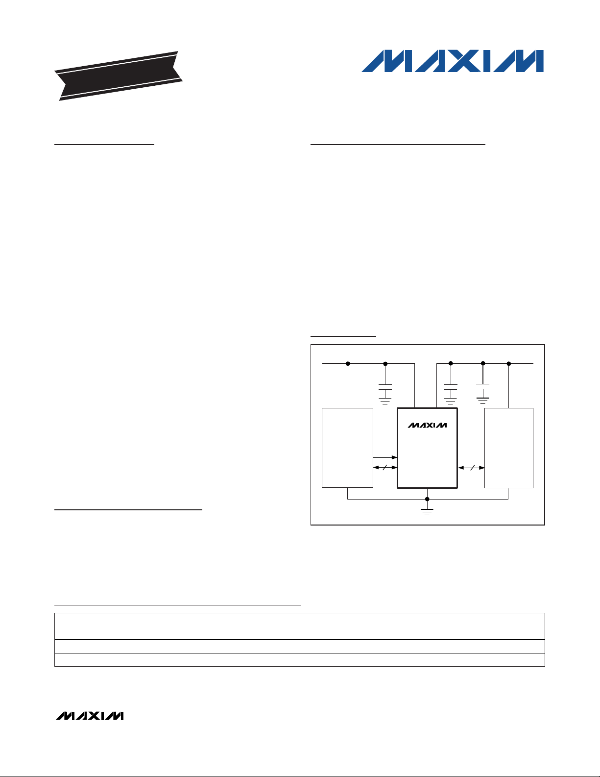
Typical Operating Circuit
Pin Configurations appear at end of data sheet.
Ordering Information/Selector Guide continued at end of data sheet.
+
Denotes a lead(Pb)-free/RoHS-compliant package.
*
EP = Exposed pad.
+3.3V
SYSTEM
+3.3V
+1.8V
0.1μF
V
+1.8V
SYSTEM
CONTROLLER
EN
DATA
GND GND GND
8
L
MAX13055E–
MAX13058E
EN
I/O V
L_
V
CC
I/O V
1μF
CC_
0.1μF
DATA
8
_ STATE
I/O V
PART
MAX13055EEWG+ Open Drain Open Drain -40°C to +85°C 24 WLP
MAX13055EETI+ Open Drain Open Drain -40°C to +85°C
DURING SHUTDOWN
L
I/O VCC_ STATE
DURING SHUTDOWN
TEMP RANGE PIN-PACKAGE
28 TQFN-EP*
Page 2
MAX13055E–MAX13058E
1.62V to 3.6V, 8-Channel, High-Speed LLT
2 _______________________________________________________________________________________
ABSOLUTE MAXIMUM RATINGS
Stresses beyond those listed under “Absolute Maximum Ratings” may cause permanent damage to the device. These are stress ratings only, and functional
operation of the device at these or any other conditions beyond those indicated in the operational sections of the specifications is not implied. Exposure to
absolute maximum rating conditions for extended periods may affect device reliability.
(Voltages referenced to GND.)
V
CC
, V
L .............................................................................
-0.3V to +4.0V
EN..........................................................................-0.3V to +4.0V
I/O V
CC
_ .....................................................-0.3V to (V
CC
+ 0.3V)
I/O V
L
_...........................................................-0.3V to (VL + 0.3V)
Short-Circuit Duration
I/O to GND..................................................................Continuous
Continuous Power Dissipation (T
A
= +70°C)
28-Pin TQFN (derate 28.6mW/°C above +70°C) .......2286mW
Junction-to-Case Thermal Resistance (θ
JC
) (Note 1)
28-Pin TQFN................................................................2.7°C/W
Junction-to-Ambient Thermal Resistance (θ
JA
) (Note 1)
24-Bump WLP ..............................................................97°C/W
28-Pin TQFN.................................................................35°C/W
Operating Temperature Range ...........................-40°C to +85°C
Junction Temperature......................................................+150°C
Storage Temperature Range .............................-65°C to +150°C
Lead Temperature (soldering, 10s) .................................+300°C
ELECTRICAL CHARACTERISTICS
(VCC= +2.2V to +3.6V, VL= +1.62V to +3.2V, EN = VL, TA= -40°C to +85°C, unless otherwise noted. Typical values are at V
CC
= +3.3V,
V
L
= +1.8V, and TA= +25°C.) (Notes 2, 3)
Note 1: Package thermal resistances were obtained using the method described in JEDEC specification JESD51-7, using a four-
layer board. For detailed information on package thermal considerations, refer to www.maxim-ic.com/thermal-tutorial
.
VL Supply Range V
VCC Supply Range V
Supply Current from V
Supply Current from V
V
CC
V
L
Current
I/O Three-State Leakage Current I
E N Inp ut Leakag e C ur r ent I
VL - VCC S hutd ow n Thr eshol d H i g hV
VL - VCC S hutd ow n Thr eshol d Low V
I/O V CC_ Pulldown Resistance
During Shutdown
I/O V L_ Pulldown Resistance
During Shutdown
I/O V L_ Pullup Current
(Normal Mode)
I/O V CC_ Pullup Current
(Normal Mode)
I/O V L_ to I/O V
ESD PROTECTION
Al l P or ts Human Body Model + 2kV
PARAMETER SYMBOL CONDITIONS MIN TYP MAX UNITS
L
CC
CC
L
Shutdown Supply Current I
Shutdown Mode Supply
_ D C Resi stance R
C C
I
QVCC
I
QVL
SHDN-VCCTA
I
SHDN-VL
LEAK
LEAK_ENTA
TH_H
TH_L
R
VCC_PD_SD
R
VL_PD_SD
I
VL_PU_
I
VCC_PU_
IOVL_IOVCC
I/O V CC_ = VCC, I/O V L_ = V
I/O V CC_ = VCC, I/O V L_ = V
= +25°C, EN = GND 0.1 2 µA
TA = +25°C, EN = GND 0.1 1
TA = +25°C, EN = V L, VCC = 0V 0.1 4
TA = +25°C, EN = GND 0.1 2 µA
= +25oC1µA
V
rising 0 0.1 x V L0.8 V
CC
V
falling 0 0.12 x V L0.8 V
CC
MAX13056E/MAX13058E 10 16.5 23 kΩ
MAX13057E/MAX13058E 10 16.5 23 kΩ
I/O VL_ = GND, I/O VCC_ = GND 20 65 µA
I/O VCC_ = GND, I/O VL_ = GND 20 65 µA
Human Body Model + 15
C C
_ Onl y
IE C 61000- 4- 2 Ai r - Gap Di schar g e, C
IE C 61000- 4- 2 Contact Di schar g e, C
1.62 3.2 V
2.2 3.6 V
L
L
40 µA
10 µA
µA
3kΩ
= 1µF + 15I/O V
V C C
= 1µF + 8
V C C
kV
Page 3
MAX13055E–MAX13058E
1.62V to 3.6V, 8-Channel, High-Speed LLT
_______________________________________________________________________________________ 3
ELECTRICAL CHARACTERISTICS (continued)
(VCC= +2.2V to +3.6V, VL= +1.62V to +3.2V, EN = VL, TA= -40°C to +85°C, unless otherwise noted. Typical values are at V
CC
= +3.3V,
V
L
= +1.8V, and TA= +25°C.) (Notes 2, 3)
LOGIC LEVELS
I/O V L_ Input-Voltage High V
I/O V L_ Input-Voltage Low V
I/O V CC_ Input-Voltage High V
I/O V CC_ Input-Voltage Low V
EN Input-Voltage High V
EN Input-Voltage Low V
I/O V L_ Output-Voltage High V
I/O V L_ Output-Voltage Low V
I/O V CC_ Output-Voltage High V
I/O V
RISE/FALL TIME ACCELERATOR STAGE
Accel er ator P ul se D ur ati on
V L Outp ut Accel er ator S our ce
Im p ed ance
V CC Outp ut Accel er ator S our ce
Im p ed ance
V L Outp ut Accel er ator S our ce
Im p ed ance
V
C C
Im p ed ance
V L Outp ut Accel er ator S i nk
Im p ed ance
V CC Outp ut Accel er ator S i nk
Im p ed ance
V L Outp ut Accel er ator S i nk
Im p ed ance
V CC Outp ut Accel er ator S i nk
Im p ed ance
PARAMETER SYMBOL CONDITIONS MIN TYP MAX UNITS
(Note 4) VL - 0.2 V
(Note 4) 0.15 V
V
-
(Note 4)
CC
0.4
(Note 4) 0.2 V
VL - 0.4 V
0.4 V
I/O V
source current = 10µA 4/5 V
L_
I/O V
si nk cur r ent = 20µA, I/O V
L_
I/O V
I/O V
source current = 10µA
CC_
si nk cur r ent = 20µA, I/O V
C C _
< 0.1V 1/5 V
C C _
< 0.1V
L_
On falling edge
On rising edge
= 1.62V 24 Ω
V
L
= 2.2V 13 Ω
V
CC
= 3.2V 11 Ω
V
L
= 3.6V 9 Ω
V
CC
= 1.62V 14 Ω
V
L
= 2.2V 11 Ω
V
CC
= 3.2V 10 Ω
V
L
= 3.6V 9 Ω
V
CC
V
L
4/5
CC
1/5
3.5 ns
_ Outp ut- V ol tage Low V
C C
Outp ut Accel er ator S our ce
IHL
ILL
IHC
ILC
IH
IL
OHL
OLL
OHC
OLC
L
V
V
V
V
V
Page 4
MAX13055E–MAX13058E
1.62V to 3.6V, 8-Channel, High-Speed LLT
4 _______________________________________________________________________________________
TIMING CHARACTERISTICS
(+2.2V ≤ VCC≤ 3.6V, +1.62V ≤ VL≤ +3.2V; C
I/OVL_
≤ 15pF, C
I/OVCC_
≤ 10pF; R
SOURCE
< 150Ω, EN = VL, TA= -40°C to +85°C,
unless otherwise noted. Typical values are at V
CC
= +3.3V, V
L
= +1.8V, and TA= +25°C.) (Notes 2, 3)
Note 2: All units are 100% production tested at TA= +25°C. Limits over the operating temperature range are guaranteed by design
and not production tested.
Note 3: V
L
must be less than or equal to VCCduring normal operation. However, VLcan be greater than VCCduring startup and
shutdown conditions. It will not latch up.
Note 4: For input thresholds, see the rise/fall time accelerator circuit in Figure 4.
PARAMETER SYMBOL CONDITIONS MIN TYP MAX UNITS
I/O V
I/O V
I/O VL_ Rise Time t
I/O VL_ Fall Time t
Propagation Delay
(Driving I/O V
Propagation Delay
(Driving I/O V
Channel-to-Channel Skew t
Propagation Delay from I/O V
to I/O V
Propagation Delay from I/O V
to I/O VL_ After EN
Maximum Data Rate
Rise Time t
CC_
Fall Time t
CC_
_)
L
_)
CC
L_
CC_
CC_
After EN
RVCC
FVCC
RVL
FVL
t
PVL-VCC
t
PVCC-VL
SKEW
t
EN-VCC
t
EN-VL
Figure 2 2.5 ns
Figure 2 2.5 ns
Figure 1 2.5 ns
Figure 1 2.5 ns
Figure 2 1 6.5 ns
Figure 1 1 6.5 ns
Figure 3 5 µs
Figure 3 5 µs
Push-pull operation 100
Open drain 1
2ns
Mbps
Page 5

MAX13055E–MAX13058E
1.62V to 3.6V, 8-Channel, High-Speed LLT
_______________________________________________________________________________________ 5
Test Circuits/Timing Diagrams
Figure 1. Push-Pull Driving I/O VL_Test Circuit and Timing
Figure 2. Push-Pull Driving I/O V
CC_
Test Circuit and Timing
V
L
EN
V
L
V
CC
MAX13055E–MAX13058E
I/O V
V
L
L_
V
CC
I/O V
50Ω
V
L
EN
V
L
V
CC
CC_
t
V
CC
RVCC
90%
I/O V
L_
50%
50%
I/O V
10%
CC_
C
IOVCC
t
PLH
t
= t
PVL-VCC
V
CC
OR t
PLH
PHL
t
RVL
I/O V
CC_
90%
50%
t
PHL
t
FVCC
t
50%
10%
FVL
MAX13055E–MAX13058E
V
L
I/O V
L_
C
IOVL_
V
CC
I/O V
CC_
50Ω
50%
10%
t
PLH
t
PVCC-VL
90%
50%
50%
90%
50%
10%
I/O V
L_
t
PHL
= t
OR t
PLH
PHL
Page 6

MAX13055E–MAX13058E
1.62V to 3.6V, 8-Channel, High-Speed LLT
6 _______________________________________________________________________________________
Test Circuits/Timing Diagrams (continued)
Figure 3. Enable Test Circuit and Timing
V
L
V
L
EN
MAX13055E–
MAX13058E
V
L
I/O V
L_
150Ω
V
L
V
L
EN
MAX13055E–
MAX13058E
V
L
C
R
LOAD
IOVL_
I/O V
L_
V
CC
V
CC
V
CC
I/O V
CC_
V
CC
V
CC
V
CC
I/O V
CC_
R
150Ω
LOAD
C
IOVCC_
V
V
I/O V
I/O V
CC_
t
EN-VCC
EN
0.5V
TIME
t
L_
EN-VL
EN
0.2V (V
0.5V (V
< 2V)
L
≥ 2V)
L
TIME
Page 7

MAX13055E–MAX13058E
1.62V to 3.6V, 8-Channel, High-Speed LLT
_______________________________________________________________________________________ 7
Typical Operating Characteristics
(VCC= +3.3V, VL= +1.8V, C
I/OVCC_
= 10pF, C
I/OVL_
= 15pF, R
SOURCE
= 50Ω, data rate = 100Mbps, push-pull driver, TA= +25°C,
unless otherwise noted.)
VL SUPPLY CURRENT vs. VCC SUPPLY
VOLTAGE (DRIVING ONE I/O VL_)
500
VL = 1.8V
460
420
380
SUPPLY CURRENT (FA)
L
V
340
300
2.2 3.6
VCC SUPPLY VOLTAGE (V)
VCC SUPPLY CURRENT vs. VL SUPPLY
VOLTAGE (DRIVING ONE I/O V
10
VCC = 3.6V
8
6
4
SUPPLY CURRENT (mA)
CC
V
2
0
1.6 3.2
VL SUPPLY VOLTAGE (V)
2.82.42.0
MAX13055E toc01
3.43.23.02.82.62.4
)
CC_
MAX13055E toc04
VL SUPPLY CURRENT vs. VL SUPPLY
VOLTAGE (DRIVING ONE I/O V
10
VCC = 3.6V
8
6
4
SUPPLY CURRENT (mA)
L
V
2
0
1.6 3.2
VL SUPPLY VOLTAGE (V)
SUPPLY CURRENT vs. TEMPERATURE
(DRIVING ONE I/O V
7
6
5
4
3
SUPPLY CURRENT (mA)
2
1
0
-40 85
I
VCC
TEMPERATURE (NC)
I
VL
2.82.42.0
CC_
VCC SUPPLY CURRENT vs. VCC SUPPLY
)
CC_
MAX13055E toc02
SUPPLY CURRENT (FA)
CC
V
)
MAX13055E toc05
SUPPLY CURRENT (mA)
603510-15
VOLTAGE (DRIVING ONE I/O VL_)
15
VL = 1.8V
12
9
6
3
0
2.2 3.6
VCC SUPPLY VOLTAGE (V)
SUPPLY CURRENT vs. TEMPERATURE
(DRIVING ONE I/O VL_)
11
10
9
8
7
6
5
4
3
2
1
0
-40 85
I
VCC
TEMPERATURE (NC)
I
VL
603510-15
MAX13055E toc03
3.43.23.02.82.62.4
MAX13055E toc06
Page 8

Typical Operating Characteristics (continued)
(VCC= +3.3V, VL= +1.8V, C
I/OVCC_
= 10pF, C
I/OVL_
= 15pF, R
SOURCE
= 50Ω, data rate = 100Mbps, push-pull driver, TA= +25°C,
unless otherwise noted.)
MAX13055E–MAX13058E
1.62V to 3.6V, 8-Channel, High-Speed LLT
8 _______________________________________________________________________________________
VL SUPPLY CURRENT vs. CAPACITIVE
LOAD ON I/O VL_ (DRIVING ONE I/O V
7
6
5
4
3
SUPPLY CURRENT (mA)
L
2
V
1
0
10 40
CAPACITIVE LOAD (pF)
RISE/FALL TIME (ns)
RISE/FALL TIME vs. CAPACITIVE
LOAD ON I/O VL_ (DRIVING I/O V
3.0
2.5
2.0
1.5
1.0
0.5
0
10 40
t
RVL
t
FVL
CAPACITIVE LOAD (pF)
)
CC_
MAX13055E toc07
3530252015
)
CC_
MAX13055E toc10
3530252015
VCC SUPPLY CURRENT vs. CAPACITIVE
LOAD ON I/O V
20
18
16
14
12
10
8
SUPPLY CURRENT (mA)
6
CC
V
4
2
0
10 40
CAPACITIVE LOAD (pF)
PROPAGATION DELAY vs. CAPACITIVE
LOAD ON I/O V
4.0
3.5
3.0
2.5
2.0
1.5
PROPAGATION DELAY (ns)
1.0
0.5
0
10 40
CAPACITIVE LOAD (pF)
(DRIVING ONE I/O VL_)
CC_
(DRIVING I/O VL_)
CC_
t
PLH
t
PHL
RISE/FALL TIME vs. CAPACITIVE
LOAD ON I/O V
1.4
1.2
MAX13055E toc08
1.0
0.8
0.6
RISE/FALL TIME (ns)
0.4
0.2
0
3530252015
10 40
(DRIVING I/O VL_)
CC_
t
RVCC
t
FVCC
CAPACITIVE LOAD (pF)
MAX13055E toc09
3530252015
PROPAGATION DELAY vs. CAPACITIVE
LOAD ON I/O V
4.0
3.5
MAX13055E toc11
3.0
2.5
2.0
1.5
PROPAGATION DELAY (ns)
1.0
0.5
353015 20 25
0
10 40
(DRIVING I/O V
L_
t
PHL
t
PLH
CAPACITIVE LOAD (pF)
)
CC_
MAX13055E toc12
353015 20 25
Page 9

MAX13055E–MAX13058E
1.62V to 3.6V, 8-Channel, High-Speed LLT
_______________________________________________________________________________________ 9
_
_
Typical Operating Characteristics (continued)
(VCC= +3.3V, VL= +1.8V, C
I/OVCC_
= 10pF, C
I/OVL_
= 15pF, R
SOURCE
= 50Ω, data rate = 100Mbps, push-pull driver, TA= +25°C,
unless otherwise noted.)
Pin Description
TYPICAL I/O VL_ DRIVING
(FREQUENCY = 25MHz, C
10ns/div
PIN
TQFN-EP WLP
1, 12, 13, 14,
24, 25, 26, 27
— N.C. No Connection. N.C. is not internally connected.
2 B1 I/O VL1 Input/Output 1 Referenced to V
3 A1 I/O VL2 Input/Output 2 Referenced to V
4 A2 I/O VL3 Input/Output 3 Referenced to V
5 A3 I/O VL4 Input/Output 4 Referenced to V
6 B3, B4, B5 GND Ground
7 A4 I/O VL5 Input/Output 5 Referenced to V
8 A5 I/O VL6 Input/Output 6 Referenced to V
9 A6 I/O VL7 Input/Output 7 Referenced to V
10 B6 I/O VL8 Input/Output 8 Referenced to V
11 C5 EN
15 C6 I/O VCC8 Input/Output 8 Referenced to V
16 D6 I/O VCC7 Input/Output 7 Referenced to V
17 D5 I/O VCC6 Input/Output 6 Referenced to V
18 D4 I/O VCC5 Input/Output 5 Referenced to V
19 C2, C3, C4 V
20 D3 I/O VCC4 Input/Output 4 Referenced to V
= 40pF)
IOVCC_
MAX13055E toc13
I/O V
1V/div
I/O V
2V/div
L_
CC
NAME FUNCTION
Enable Control Input. Drive EN high for normal operation. Drive EN low for shutdown
mode.
CC
+2.2V to +3.6V Power-Supply Voltage. Bypass VCC with 1µF and 0.1µF ceramic
capacitors located as close to the device as possible.
TYPICAL I/O V
(FREQUENCY = 25MHz, C
10ns/div
CC_
DRIVING
= 15pF)
IOVL_
MAX13055E toc14
I/O V
2V/div
I/O V
1V/div
CC
L_
L
L
L
L
L
L
L
L
CC
CC
CC
CC
CC
Page 10

MAX13055E–MAX13058E
1.62V to 3.6V, 8-Channel, High-Speed LLT
10 ______________________________________________________________________________________
Functional Diagram
Pin Description (continued)
PIN
TQFN-EP WLP
21 D2 I/O VCC3 Input/Output 3 Referenced to V
22 D1 I/O VCC2 Input/Output 2 Referenced to V
23 C1 I/O VCC1 Input/Output 1 Referenced to V
28 B2 V
— — EP Exposed Pad. Connect EP to GND.
NAME FUNCTION
CC
CC
CC
+1.62V to +3.2V Logic-Supply Voltage. Bypass VL with a 0.1µF ceramic capacitor
L
located as close to the device as possible.
V
L
MAX13055E–MAX13058E
CHANNEL 1
I/O VL1 I/O VCC1
I/O VL2 I/O VCC2
I/O VL3 I/O VCC3
I/O VL4 I/O VCC4
I/O VL7 I/O VCC7
I/O VL8 I/O VCC8
EN
NOTE: EXTERNAL PULLUP RESISTORS NOT RECOMMENDED ON I/O LINES.
CHANNEL 2
CHANNEL 3
CHANNEL 4
CHANNEL 5I/O VL5 I/O VCC5
CHANNEL 6I/O VL6 I/O VCC6
CHANNEL 7
CHANNEL 8
GND
V
CC
Page 11

MAX13055E–MAX13058E
Detailed Description
The MAX13055E–MAX13058E 8-channel, bidirectional
level translators provide the level shifting necessary for
100Mbps data transfer in multivoltage systems. The
MAX13055E–MAX13058E are ideally suited for level
translation in systems with 8 channels. Externally
applied voltages, V
CC
and VL, set the logic levels on
either side of the device. Logic-high signals presented
on the VLside of the device appear as a logic-high signal on the V
CC
side of the device and vice versa.
The MAX13055E–MAX13058E operate at full speed
with external drivers that source as little as 4mA output
current. Each I/O channel is pulled up to VCCor VLby
an internal 40µA current source, allowing the
MAX13055E–MAX13058E to be driven by either pushpull or open-drain drivers.
The MAX13055E–MAX13058E feature an enable (EN)
input that places the devices into a low-power shutdown mode when driven low. The MAX13055E–
MAX13058E feature an automatic shutdown mode that
disables the part when VCCis less than VL. The state of
I/O V
CC
_ and I/O VL_ during shutdown is chosen by
selecting the appropriate part version (see the
Ordering
Information/Selector Guide
).
The MAX13055E–MAX13058E operate with V
CC
voltages from +2.2V to +3.6V and VLvoltages from +1.62V
to +3.2V.
Level Translation
For proper operation, ensure that +2.2V ≤ VCC≤ +3.6V,
+1.62V ≤ VL≤ VCC- 0.2V. When power is supplied to
V
L
while VCCis missing or less than VL, the
MAX13055E–MAX13058E automatically enter a lowpower mode. The devices also enters shutdown mode
when VEN= 0V. This allows VCCto be disconnected
and still have a known state on I/O VL_. The maximum
data rate depends heavily on the load capacitance
(see the Rise/Fall Time vs. Capacitive Load graphs in
the
Typical Operating Characteristics
), output imped-
ance of the driver, and the operating voltage range.
Input Requirements
The MAX13055E–MAX13058E architecture is based on
an nMOS pass gate and rise/fall time accelerator stages
(Figure 4). The accelerators are active only when there
is a rising/falling edge on a given I/O. A short pulse is
then generated where the output accelerator stages
become active and charges/discharges the capacitance at the I/Os. Due to its architecture, both input
stages become active during the one-shot pulse. This
can lead to current feeding into the external source that
is driving the translator. However, this behavior helps to
speed up the transition on the driven side.
The MAX13055E–MAX13058E have internal current
sources capable of sourcing 40µA to pull up the I/O
lines. These internal pullup current sources allow the
inputs to be driven with open-drain drivers as well as
push-pull drivers. It is not recommended to use external
pullup resistors on the I/O lines. The architecture of the
MAX13055E–MAX13058E permits either side to be driven with a minimum of 4mA drivers or larger.
Figure 4. Simplified Functional Diagram for One I/O Line
1.62V to 3.6V, 8-Channel, High-Speed LLT
______________________________________________________________________________________ 11
V
L
I/O V
L_
RISE/FALL TIME
ACCELERATOR
ONE-SHOT
ONE-SHOT
V
RISE/FALL TIME
ACCELERATOR
ONE-SHOT
V
BIAS
ONE-SHOT
CCVCC
I/O V
CC_
Page 12

MAX13055E–MAX13058E
1.62V to 3.6V, 8-Channel, High-Speed LLT
12 ______________________________________________________________________________________
Output Load Requirements
The MAX13055E–MAX13058E I/O are designed to drive
CMOS inputs. Do not load the I/O lines with a resistive
load less than 25kΩ. Do not place an RC circuit at the
input of these devices to slow down the edges. If a
slower rise/fall time is required, refer to the MAX3000E/
MAX3001E logic-level translator data sheet.
Shutdown Mode
The MAX13055E–MAX13058E feature an enable (EN)
input that places the devices into a low-power shutdown
mode when driven low. The MAX13055E–MAX13058E
feature an automatic shutdown mode that disables the
part when VCCis unconnected or less than VL.
Applications Information
Layout Recommendations
Use standard high-speed layout practices when laying
out a board with the MAX13055E–MAX13058E. For
example, to minimize line coupling, place all other signal
lines not connected to the MAX13055E–MAX13058E at
least 1x the substrate height of the PCB away from the
input and output lines of the MAX13055E–MAX13058E.
Power-Supply Decoupling
To reduce ripple and the chance of introducing data
errors, bypass VL and VCCto ground with 0.1µF ceramic capacitors. Place all capacitors as close to the
power-supply inputs as possible. For full ESD protection, bypass VCCwith a 1µF ceramic capacitor located
as close to the VCCinput as possible.
Unidirectional vs. Bidirectional
Level Translator
The MAX13055E–MAX13058E bidirectional level translators can operate as a unidirectional device to translate signals without inversion. These devices provide a
small solution for unidirectional level translation without
inversion.
ESD Test Conditions
ESD performance depends on a variety of conditions.
Contact Maxim for a reliability report that documents
test setup, test methodology, and test results.
Use with External Pullup/
Pulldown Resistors
Due to the architecture of the MAX13055E–
MAX13058E, it is not recommended to use external
pullup or pulldown resistors on the bus. In certain applications, the use of external pullup or pulldown resistors
is desired to have a known bus state when there is no
active driver on the bus. The MAX13055E–MAX13058E
include internal pullup current sources that set the bus
state when the device is enabled. In shutdown mode,
the state of I/O V
CC
_ and I/O VL_ is dependent on the
selected part version (see the
Ordering Information/
Selector Guide
).
Open-Drain Signaling
The MAX13055E–MAX13058E are designed to pass
open-drain as well as CMOS push-pull signals. When
used with open-drain signaling, the rise time is dominated
by the interaction of the internal pullup current source and
the parasitic load capacitance. The MAX13055E–
MAX13058E include internal rise-time accelerators to
speed up transitions, eliminating any need for external
pullup resistors. For applications such as I2C or 1-Wire
®
that require an external pullup resistor, refer to the
MAX3378E and MAX3396E data sheets.
Human Body Model
Figure 5a shows the Human Body Model and Figure 5b
shows the current waveform it generates when discharged into a low impedance. This model consists of a
100pF capacitor charged to the ESD voltage of interest,
which is then discharged into the test device through a
1.5kΩ resistor.
IEC 61000-4-2
The IEC 61000-4-2 standard covers ESD testing and performance of finished equipment; it does not specifically
refer to integrated circuits. The MAX13055E–MAX13058E
help in designing equipment that meets level 4 (the highest level) of IEC 61000-4-2, without the need for additional ESD-protection components. The major difference
between tests done using the Human Body Model and
IEC 61000-4-2 is higher peak current in IEC 61000-4-2,
because series resistance is lower in the IEC 61000-4-2
model. Hence, the ESD withstand voltage measured to
IEC 61000-4-2 is generally lower than that measured
using the Human Body Model. Figure 6a shows the IEC
61000-4-2 model and Figure 6b shows the current waveform for the ±8kV, IEC 61000-4-2, level 4, ESD Contact
Discharge Method.
The Air Gap Method involves approaching the device
with a charged probe. The Contact Discharge Method
connects the probe to the device before the probe is
energized.
Chip Information
PROCESS: CMOS
1-Wire is a registered trademark of Maxim Integrated Products,
Inc.
Page 13

MAX13055E–MAX13058E
1.62V to 3.6V, 8-Channel, High-Speed LLT
______________________________________________________________________________________ 13
Figure 5b. Human Body Current Waveform
Figure 5a. Human Body ESD Test Model
Figure 6b. IEC 61000-4-2 ESD Generator Current Waveform
Figure 6a. IEC 61000-4-2 ESD Test Model
Ordering Information/Selector Guide (continued)
+
Denotes a lead(Pb)-free/RoHS-compliant package.
*
EP = Exposed pad.
**
Future product—contact factory for availability.
R
D
1500Ω
DISCHARGE
RESISTANCE
STORAGE
CAPACITOR
HIGH-
VOLTAGE
DC
SOURCE
R
C
1MΩ
CHARGE-CURRENT-
LIMIT RESISTOR
C
100pF
s
R
D
330Ω
DISCHARGE
RESISTANCE
STORAGE
CAPACITOR
HIGH-
VOLTAGE
DC
SOURCE
R
C
50MΩ to 100MΩ
CHARGE-CURRENT-
LIMIT RESISTOR
C
s
150pF
DEVICE
UNDER
TEST
DEVICE
UNDER
TEST
AMPERES
IP 100%
90%
36.8%
10%
0
0
t
RL
I
R
TIME
t
DL
CURRENT WAVEFORM
I
100%
90%
PEAK
I
10%
t
= 0.7ns to 1ns
R
30ns
60ns
PEAK-TO-PEAK RINGING
(NOT DRAWN TO SCALE)
t
I/O V
_ STATE
PART
DURING SHUTDOWN
L
MAX13056EEWG+** Open Drain 10kΩ to GND -40°C to +85°C 24 WLP
MAX13056EETI+** Open Drain 10kΩ to GND -40°C to +85°C 28 TQFN-EP*
MAX13057EEWG+** 10kΩ to GND Open Drain -40°C to +85°C 24 WLP
MAX13057EETI+** 10kΩ to GND Open Drain -40°C to +85°C 28 TQFN-EP*
MAX13058EEWG+ 10kΩ to GND 10kΩ to GND -40°C to +85°C 24 WLP
MAX13058EETI+ 10kΩ to GND 10kΩ to GND -40°C to +85°C 28 TQFN-EP*
I/O VCC_ STATE
DURING SHUTDOWN
TEMP RANGE PIN-PACKAGE
Page 14

MAX13055E–MAX13058E
1.62V to 3.6V, 8-Channel, High-Speed LLT
Maxim cannot assume responsibility for use of any circuitry other than circuitry entirely embodied in a Maxim product. No circuit patent licenses are
implied. Maxim reserves the right to change the circuitry and specifications without notice at any time.
14
____________________Maxim Integrated Products, 120 San Gabriel Drive, Sunnyvale, CA 94086 408-737-7600
© 2009 Maxim Integrated Products Maxim is a registered trademark of Maxim Integrated Products, Inc.
Pin Configurations
PACKAGE TYPE PACKAGE CODE DOCUMENT NO.
24 WLP W241B2-1
21-0219
28 TQFN T283555-1
21-0184
Package Information
For the latest package outline information and land patterns, go to www.maxim-ic.com/packages.
TOP VIEW
1
CC
I/O V
N.C.
24 23 22 21 20 19 18 17 16 15
25
N.C.
26
N.C.
N.C.
V
MAX13055E–MAX13058E
27
28
L
+
12345678910
1
L
N.C.
I/O V
CC
I/O V
2
L
I/O V
CC
I/O V
3
L
I/O V
CC
I/O V
4
L
I/O V
V
GND
CC
CC
I/O V
5
L
I/O V
CC
I/O V
*EP
6
L
I/O V
CC
I/O V
7
L
I/O V
CC
I/O V
14
13
12
11
8
L
I/O V
N.C.
N.C.
N.C.
EN
8
7
6
5
4
3
2
TQFN
*CONNECT EXPOSED PAD TO GND.
TOP VIEW
(BUMPS ON BOTTOM)
MAX13055E–MAX13058E
A
V
CC
CC
CC
BC
I/O VL1I/O VCC1I/O VCC2 I/O VL2
I/O VL3V
L
GNDV
I/O VL5GNDV
GNDENI/O VCC6 I/O VL6
I/O VL7I/O VL8I/O VCC8I/O VCC7
D
I/O VCC3
I/O VCC4 I/O VL4
I/O VCC5
WLP
+
1
2
3
4
5
6
 Loading...