

Page 1
General Description
The MAX13051 ±80V fault-protected CAN transceiver
with autobaud is ideal for device net and other industrial network applications where overvoltage protection is
required. The MAX13051 provides a link between the
CAN protocol controller and the physical wires of the
bus lines in a control area network (CAN).
The MAX13051 features three different modes of operation: high speed, slope control, and standby. Highspeed mode allows data rates up to 1Mbps. The
slope-control mode can be used to program the slew
rate of the transmitter for data rates of up to 500kbps,
reducing the effects of EMI and allowing the use of
unshielded-twisted or parallel cable. In standby mode,
the transmitter shuts off and a low-power receiver monitors the bus, waiting for a wake-up signal.
The MAX13051 provides a transmitter data (TXD) dominant timeout function that prevents erroneous CAN controllers from clamping the bus to a dominant level if the
TXD input is held low for greater than 1ms. The
MAX13051 also provides an autobaud feature allowing
the microcontroller to compute the incoming baud rate
without destroying CAN protocol communication. The
MAX13051 input common-mode range is greater than
±12V, exceeding the ISO 11898 specification of -2V to
+7V, and features ±6kV Human Body Model protection,
making these devices ideal for harsh environments. The
MAX13051 is available in an 8-pin SO package and is
specified from the -40°C to +85°C and -40°C to +125°C
temperature ranges.
Applications
Industrial Networks
Device Net Nodes
Telecom
HVAC
Features
♦ Fully Compatible with the ISO 11898 Standard
♦ Autobaud Mode
♦ Short-Circuit Protection
♦ High-Speed Operation Up to 1Mbps
♦ Slope-Control Mode
♦ Low-Current Standby Mode
♦ Thermal Shutdown
♦ Transmit Data Dominant Timeout
♦ ±6kV Human Body Model ESD Protection
♦ Greater than ±12V Common-Mode Range
MAX13051
±80V Fault-Protected Can Transceiver
with Autobaud
________________________________________________________________ Maxim Integrated Products 1
19-3500; Rev 0; 11/04
For pricing, delivery, and ordering information, please contact Maxim/Dallas Direct! at
1-888-629-4642, or visit Maxim’s website at www.maxim-ic.com.
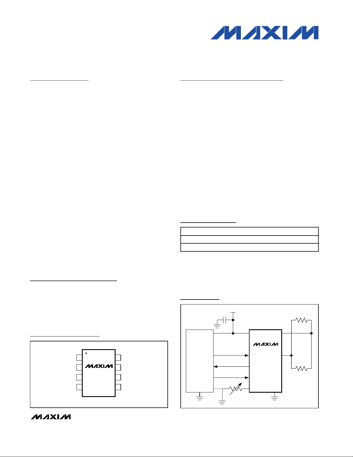
CANL
AUTOBAUDRXD
1
2
87RS
CANHGND
V
CC
TXD
SO
TOP VIEW
3
4
6
5
MAX13051
Pin Configuration
Typical Operating Circuit
Ordering Information
PART TEMP RANGE PIN-PACKAGE
MAX13051ESA -40°C to +85°C 8 SO
MAX13051ASA -40°C to +125°C 8 SO
CAN
CONTROLLER
GND GND
V
CC
0.1µF
TX0
RX0
I/O
I/O
16kΩ TO 200kΩ
V
CC
TXD
RXD
AUTOBAUD
RS
CANH
MAX13051
CANL
120Ω
120Ω
Page 2
MAX13051
±80V Fault-Protected Can Transceiver
with Autobaud
2 _______________________________________________________________________________________
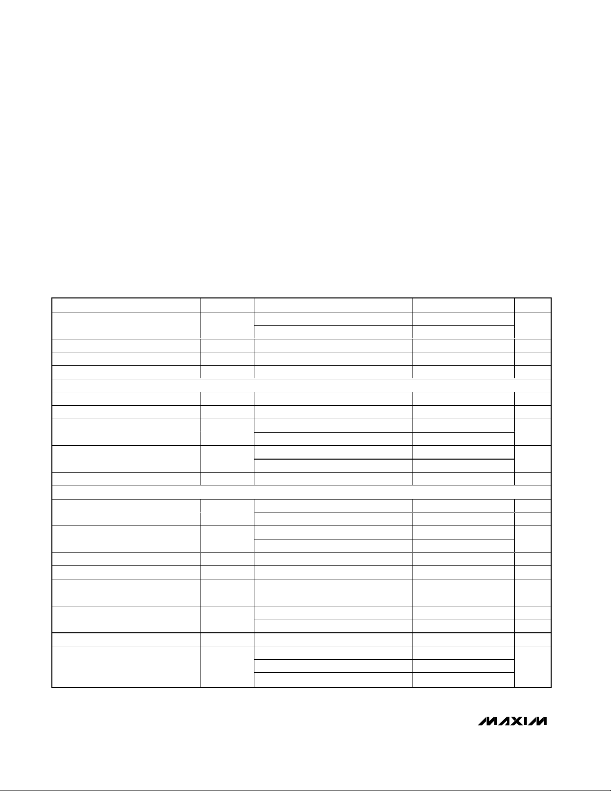
ABSOLUTE MAXIMUM RATINGS
Stresses beyond those listed under “Absolute Maximum Ratings” may cause permanent damage to the device. These are stress ratings only, and functional
operation of the device at these or any other conditions beyond those indicated in the operational sections of the specifications is not implied. Exposure to
absolute maximum rating conditions for extended periods may affect device reliability.
(All voltages referenced to GND.)
V
CC .......................................................................................
-0.3V to +6V
RS...............................................................-0.3V to (V
CC
+ 0.3V)
TXD, RXD, AUTOBAUD............................................-0.3V to +6V
CANH, CANL .......................................................................±80V
Continuous Power Dissipation (T
A
= +70°C)
8-Pin SO (derate 5.9mW/°C above +70°C) .................470mW
Operating Temperature Range .........................-40°C to +125°C
Junction Temperature......................................................+150°C
Storage Temperature Range .............................-65°C to +150°C
Lead Temperature (soldering, 10s) ................................+300°C
DC ELECTRICAL CHARACTERISTICS
(V
CC
= +5V ±5%, TA= T
MIN
to T
MAX
, unless otherwise noted. Typical values are at VCC= +5V, TA= +25°C.) (Note 1)
PARAMETER SYMBOL CONDITIONS MIN TYP MAX UNITS
Supply Current I
Standby Current I
Thermal-Shutdown Threshold V
Thermal-Shutdown Hysteresis 13 °C
INPUT LEVELS (TXD, AUTOBAUD)
High-Level Input Voltage V
Low-Level Input Voltage V
High-Level Input Current I
Low-Level Input Current I
Input Capacitance C
CANH, CANL TRANSMITTER
Recessive Bus Voltage
Recessive Output Current
CANH Output Voltage V
CANL Output Voltage V
Matching Between CANH and CANL
Output Voltage
Differential Output
(V
CANH
- V
CANL
)
CANH Short-Circuit Current I
CC
STANDBY
TSH
IH
IL
IH
IL
IN
V
CANH
V
CANL Standby mode, no load -100 +100 mV
I
CANH
I
CANL -32V < V
CANH
CANL
∆DOM
V
DIFF
CANHSCVCANH
CANLSC
Dominant, RL = 60Ω 72
Recessive 15
V
= V
TXD
V
AUTOBAUD
V
= GND -300 -100
TXD
V
AUTOBAUD
Normal mode, V
,
-76V < V
,
V
= 0, dominant 3.0 4.5 V
TXD
V
= 0, dominant 0.50 1.75 V
TXD
V
= 0, dominant, TA = +25°C
TXD
(V
CANH
Dominant, V
Recessive, V
V
= 5V, V
CANL
V
= 40V, V
CANL
V
= 76V, V
CANL
+165 °C
2V
CC
= V
CC
-5 +5
+5 +15
= GND -5 +5
10 pF
= VCC, no load 2 3 V
TXD
, V
CANH
CANH
+ V
= 0, V
CANL
TXD
TXD
TXD
< +76V ±3
CANL
, V
< +32V -2.5 +2.5
CANL
) -V
CC
-100 +150 mV
= 0, 45Ω < RL < 60Ω 1.5 3.0 V
= VCC, no load -50 +50 mV
= 0 -100 -70 -45 mA
= 0 40 60 90
TXD
= 0 40 60 90CANL Short-Circuit Current I
TXD
= 0 63
TXD
25 µA
0.8 V
mA
µA
µA
mA
mA
Page 3
MAX13051
±80V Fault-Protected Can Transceiver
with Autobaud
_______________________________________________________________________________________ 3
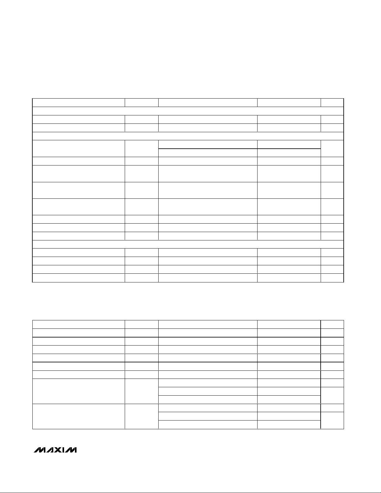
DC ELECTRICAL CHARACTERISTICS (continued)
(V
CC
= +5V ±5%, TA= T
MIN
to T
MAX
, unless otherwise noted. Typical values are at VCC= +5V, TA= +25°C.) (Note 1)
)
TIMING CHARACTERISTICS
(VCC= +5V ±5%, RL= 60Ω, CL= 100pF, TA= T
MIN
to T
MAX
, unless otherwise noted. Typical values are at VCC= +5V and TA= +25°C.)
PARAMETER SYMBOL CONDITIONS MIN TYP MAX UNITS
RXD OUTPUT LEVELS
RXD High Output Voltage Level V
RXD Low Output Voltage Level
DC BUS RECEIVER (V
Differential Input Voltage V
Differential Input Hysteresis V
Common-Mode Input Resistance R
Matching Between CANH and CANL
Common-Mode Input Resistance
Differential Input Resistance R
Common-Mode Input Capacitance V
Differential Input Capacitance V
Input Leakage Current I
SLOPE CONTROL (RS )
Input Voltage for High-Speed Mode V
Input Voltage for Standby V
Slope-Control Mode Voltage V
High-Speed Mode Current I
= VCC, CANH and CANL externally driven)
TXD
OH
V
OL
DIFF
DIFF (HYST
ICM
R
IC_MATCH
DIFF
LI
IL_RS
IH_RS
SLOPE
IL_RS
I = -100µA 0.8 x V
I = 5mA 0.4 V
-12V < V
-12V < V
Normal mode, -12V < V
Normal or standby mode,
V
CANH
Normal or standby mode,
V
CANH
= V
TXD
= V
TXD
V
= 0, V
CC
-200µA < IRS < 10µA 0.4 x V
VRS = 0 -500 µA
< +12V 0.5 0.7 0.9
CM
< +12V, standby mode 0.5 1.1
CM
= V
- V
CANL
CANL
CC
CC
CANH
= ±12V
= 1V
= V
CC
< +12V 70 mV
CM
V
15 35 kΩ
-3 +3 %
25 75 kΩ
20 pF
10 pF
= 5V -5 +5 µA
CANL
0.3 x V
0.75 x V
CC
CC
0.6 x V
CC
CC
CC
V
V
V
V
V
Delay TXD to Bus Active t
Delay TXD to Bus Inactive t
Delay Bus to Receiver Active t
Delay Bus to Receiver Inactive
Delay TXD to RXD Active t
Delay TXD to RXD Inactive T
Delay TXD to RXD Active (Dominant
Loop Delay) Slew-Rate Controlled
Delay TXD to RXD Inactive (Loop
Delay) Slew-Rate Controlled
PARAMETER SYMBOL CONDITIONS MIN TYP MAX UNITS
t
ONLOOP_S
t
OFFLOOP_S
ONTXD
OFFTXD
ONRXD
t
OFFRXD
ONLOOPVRS
OFFLOOPVRS
V
RS
V
RS
V
RS
V
RS
RRS = 24kΩ (500kbps) 280 450 ns
RRS = 100kΩ (125kbps) 0.82 1.6
RRS = 180kΩ (62.5kbps) 1.37 5
RRS = 24kΩ (500kbps) 386 600 ns
RRS = 100kΩ (125kbps) 0.74 1.6
RRS = 180kΩ (62.5kbps) 0.97 5
= 0 (Figure 1) 66 110 ns
= 0 (Figure 1) 61 95 ns
= 0 (Figure 1) 54 115 ns
= 0 (Figure 1) 46 160 ns
= 0 (Figure 1) 121 255 ns
= 0 (Figure 1) 108 255 ns
µs
µs
Page 4
MAX13051
±80V Fault-Protected Can Transceiver
with Autobaud
4 _______________________________________________________________________________________
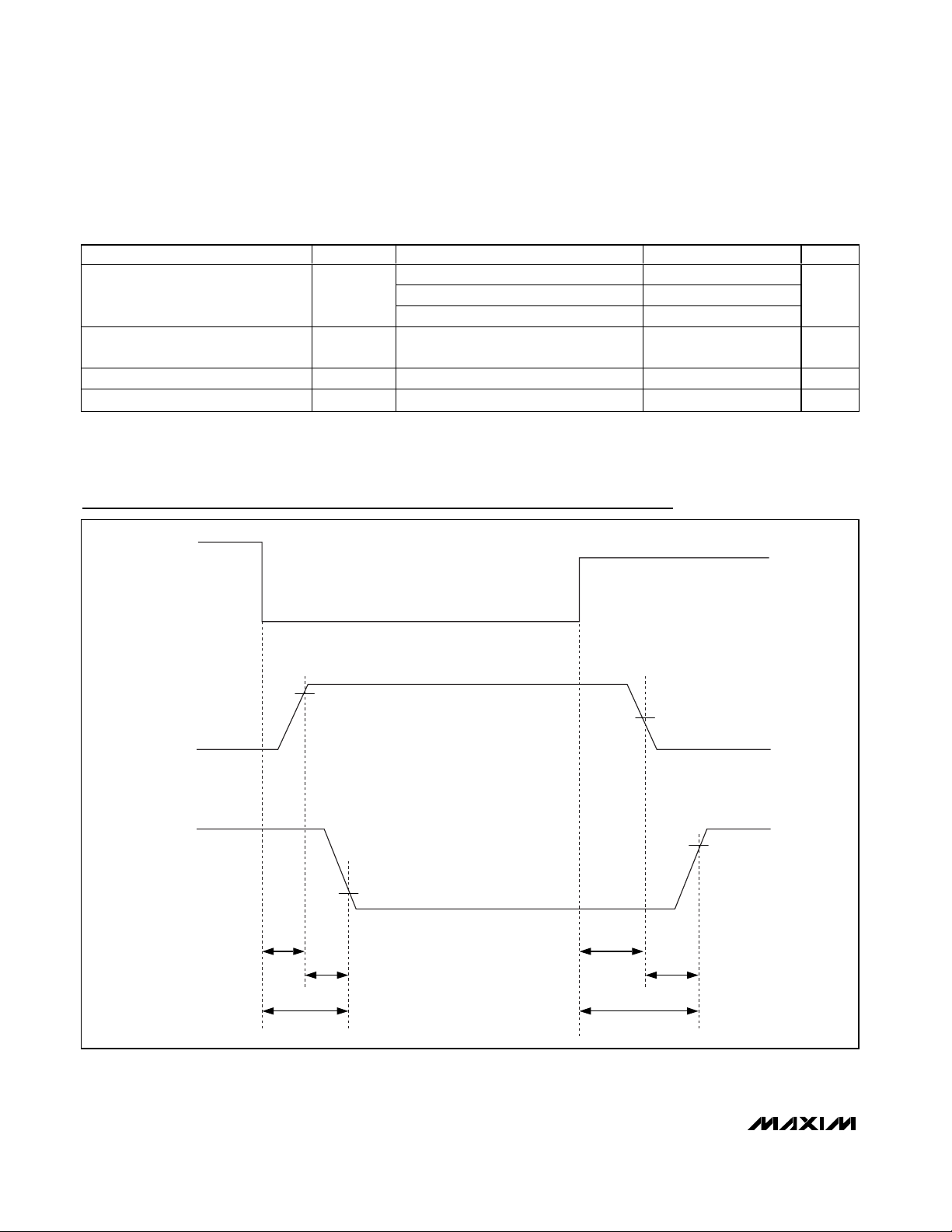
Note 1: All currents into device are positive and all currents out of the device are negative. All voltages are referenced to device
ground unless otherwise noted.
TIMING CHARACTERISTICS (continued)
(VCC= +5V ±5%, RL= 60Ω, CL= 100pF, TA= T
MIN
to T
MAX
, unless otherwise noted. Typical values are at VCC= +5V and TA= +25°C.)
Figure 1. Timing Diagram
Timing Diagrams
PARAMETER SYMBOL CONDITIONS MIN TYP MAX UNITS
Differential-Output Slew Rate
Dominant Time for Wake-Up Through
Bus (Figure 2)
TXD Dominant Timeout t
ESD Protection Human Body Model (CANH, CANL) 6 kV
TXD
|SR|
t
WAKE
DOM
RRS = 24kΩ (500kbps) 10
RRS = 100kΩ (125kbps) 2.7
RRS = 180kΩ (62.5kbps) 1.6
Standby mode, V
V
= 0 0.3 0.6 1.0 ms
TXD
= 3V 0.75 1.5 3.00 µs
DIFF
V/µs
V
DIFF
RXD
t
ONTXD
t
ONLOOP
0.9V
t
ONRXD
0.3 x V
DOMINANT
0.5V
RECESSIVE
0.7 x V
CC
CC
t
OFFTXD
t
OFFRXD
t
OFFLOOP
Page 5

MAX13051
±80V Fault-Protected Can Transceiver
with Autobaud
_______________________________________________________________________________________ 5
Figure 2. Timing Diagram for Standby and Wake-Up Signal
Timing Diagrams (continued)
Typical Operating Characteristics
(VCC= +5V, RL= 60Ω, CL= 100pF, TA= +25°C, unless otherwise specified.)
SLEW RATE
vs. R
RS
AT 100kbps
MAX13051 toc01
RRS (kΩ)
SLEW RATE (V/µs)
18016014012010080604020
5
10
15
20
25
30
0
0 200
RECESSIVE
DOMINANT
SUPPLY CURRENT
vs. DATA RATE
MAX13051 toc02
DATA RATE (kbps)
SUPPLY CURRENT (mA)
900800700600500400300200100
20
25
30
35
40
15
0 1000
TA = +25°CTA = -40°C
TA = +125°C
STANDBY SUPPLY CURRENT
vs. TEMPERATURE (RS = V
CC
)
MAX13051 toc03
TEMPERATURE (°C)
STANDBY SUPPLY CURRENT (µA)
603510-15
11
12
13
14
15
16
17
18
19
20
10
-40 85
STANDBY MODE
DOMINANT
V
DIFF
RXD
0.9V
t
WAKE
Page 6

MAX13051
±80V Fault-Protected Can Transceiver
with Autobaud
6 _______________________________________________________________________________________
Typical Operating Characteristics (continued)
(VCC= +5V, RL= 60Ω, CL= 100pF, TA= +25°C, unless otherwise specified.)
RECEIVER PROPAGATION DELAY
vs. TEMPERATURE
MAX13051 toc04
TEMPERATURE (°C)
RECEIVER PROPAGATION DELAY (ns)
1007525 500-25
10
20
30
40
50
60
70
80
90
100
0
-50 125
RECESSIVE
RRS = GND, DATA RATE = 100kbps
DOMINANT
DRIVER PROPAGATION DELAY
vs. TEMPERATURE
MAX13051 toc05
TEMPERATURE (°C)
DRIVER PROPAGATION DELAY (ns)
603510-15
20
40
60
80
100
120
140
160
180
200
0
-40 85
RECESSIVE
DOMINANT
RRS = GND, DATA RATE = 100kbps
RECEIVER OUTPUT LOW
vs. OUTPUT CURRENT
MAX13051 toc06
OUTPUT CURRENT (mA)
VOLTAGE RXD (V)
2015105
0.2
0.4
0.6
0.8
1.0
1.2
1.4
0
0
TA = -40°C
TA = +125°C
TA = +25°C
RECEIVER OUTPUT HIGH
vs. OUTPUT CURRENT
MAX13051 toc07
OUTPUT CURRENT (mA)
RECEIVER OUTPUT HIGH (V
CC
- RXD) (V)
764 52 31
0.2
0.4
0.6
0.8
1.0
1.2
1.4
1.6
1.8
2.0
0
08
TA = -40°C
TA = +125°C
TA = +25°C
DIFFERENTIAL VOLTAGE
vs. DIFFERENTIAL LOAD
MAX13051 toc08
DIFFERENTIAL LOAD RL (Ω)
DIFFERENTIAL VOLTAGE (V)
26022018014010060
0.5
1.0
1.5
2.0
2.5
3.0
3.5
0
20 300
TA = +125°C
TA = -40°C
TA = +25°C
RECEIVER PROPAGATION DELAY
MAX13051 toc09
200ns
V
DIFF
(1V/div)
RXD
(2V/div)
DRIVER PROPAGATION DELAY,
(with R
RS
= 24kΩ, 75kΩ AND 100kΩ)
MAX13051 toc10
1.00µs
TXD
(5V/div)
V
DIFF
(2V/div)
R
RS
= 24kΩ
V
DIFF
(2V/div)
R
RS
= 75kΩ
V
DIFF
(2V/div)
R
RS
= 100kΩ
Page 7

MAX13051
±80V Fault-Protected Can Transceiver
with Autobaud
_______________________________________________________________________________________ 7
Typical Operating Characteristics (continued)
(VCC= +5V, RL= 60Ω, CL= 100pF, TA= +25°C, unless otherwise specified.)
DRIVER PROPAGATION DELAY,
(R
RS
= GND)
MAX13051 toc11
200ns/div
TXD
(2V/div)
V
DIFF
(1V/div)
LOOPBACK PROPAGATION DELAY
vs. R
RS
MAX13051 toc12
RRS (kΩ)
LOOPBACK PROPAGATION DELAY (µs)
18016014012010080604020
0.2
0.4
0.6
0.8
1.0
1.2
1.4
0
0200
RECESSIVE
DOMINANT
PIN NAME FUNCTION
1 TXD Transmit Data Input. TXD is a CMOS/TTL-compatible input from a CAN controller.
2 GND Ground
3VCCSupply Voltage. Bypass VCC to GND with a 0.1µF capacitor.
4 RXD
Receive Data Output. RXD is a CMOS/TTL-compatible output from the physical bus lines CANH and CANL.
5
Autobaud Input. Drive AUTOBAUD low for normal operation. Drive AUTOBAUD high for autobaud
operation. When operating in autobaud mode, TXD is looped back to RXD without applying a differential
signal at CANH and CANL.
6 CANL CAN Bus Line Low
7 CANH CAN Bus Line High
8RS
Mode-Select Input. Drive RS low or connect to GND for high-speed operation. Connect a resistor between
RS and GND to control output slope. Drive RS high to put into standby mode.
Pin Description
AUTOBAUD
Page 8

MAX13051
Detail Description
±80V Fault Tolerant
The MAX13051 features ±80V fault protection. This
extended voltage range of CANH and CANL allows
communication in high-voltage systems up to 80V.
Operating Modes
High-Speed Mode
The MAX13051 can achieve transmission rates of up to
1Mbps when operating in high-speed mode. To operate in high-speed mode, short RS to ground.
Slope-Control Mode
Connect a resistor from RS to ground to select slopecontrol mode (Table 1). In slope-control mode, CANH
and CANL slew rates are controlled by the resistor,
(16kΩ≤R
RS
≤ 200kΩ), connected between RS and
GND. Controlling the rise and fall slopes reduces highfrequency EMI and allows the use of an unshieldedtwisted pair or a parallel pair of wires as bus lines. The
slew rate can be approximated using the formula
below:
where, SR is the desired slew rate and R
RS
is in kΩ.
Standby Mode
In standby mode (RS = high), the transmitter is
switched off and the receiver is switched to a low-current/low-speed state. The supply current reduces to
15µA to detect and recognize a wake-up event on the
bus line. During standby mode, the bus line is monitored with a low-differential comparator. Once the comparator detects a dominant bus level greater than
t
WAKE
, RXD pulls low.
Autobaud Mode
The MAX13051 logic-controlled autobaud input allows
a microcontroller to compute the incoming baud rate
without destroying CAN protocol communication. When
operating in autobaud mode, TXD is looped back to
RXD without applying a differential signal at CANH and
CANL. See Figure 4.
SR V s
R
RS
/ µ
()
≈
250
±80V Fault-Protected Can Transceiver
with Autobaud
8 _______________________________________________________________________________________
Figure 3. MAX13051 Functional Diagram
V
CC
AUTOBAUD
TXD
RXD
RS
V
CC
TIMEOUT
AND SLOPE-
CONTROL
MODE
AUTOBAUD
CIRCUITRY
ENABLE
MUX
MAX13051
THERMAL
SHUTDOWN
WAKE-UP MODE
CONTROL
WAKE-UP
FILTER
DRIVER
CANH
CANL
GND
Page 9

Transmitter
The transmitter converts a single-ended input (TXD)
from the CAN controller to differential outputs for the
bus lines (CANH, CANL). The truth table for the transmitter and receiver is given in Table 2.
TXD Dominant Timeout
The MAX13051 provides a transmitter-dominant timeout
that prevents erroneous CAN controllers from clamping
the bus to a dominant level by maintaining a continuous
low TXD signal. When the TXD remains in the dominant
state for greater than 1ms (max), the transmitter
becomes disabled, driving the bus line to a recessive
state (Figure 5). After a dominant timeout fault, the
MAX13051’s transmitter becomes enabled upon
detecting a rising edge at TXD.
Receiver
The receiver reads differential inputs from the bus lines
(CANH, CANL) and transfers this data as a singleended output (RXD) to the CAN controller. It consists of
a comparator that senses the difference, V
DIFF
=
(CANH - CANL), with respect to an internal threshold of
0.7V. If this difference is positive, (V
DIFF
> 0.9V), a
logic-low is present at RXD. If negative, (V
DIFF
< 0.5V),
a logic-high is present. The receiver always echoes the
CAN bus data when not operating in autobaud mode.
MAX13051
±80V Fault-Protected Can Transceiver
with Autobaud
_______________________________________________________________________________________ 9
Table 1. Mode Selection Truth Table
Figure 4. MAX13051 Autobaud Timing Diagram
Table 2. Transmitter and Receiver Truth Table when Not Connected to the Bus
*Common-mode input resistance.
CONDITION FORCED AT PIN RS MODE RESULTING CURRENT AT RS
VRS ≤ 0.3V x V
0.4V x VCC < VRS ≤ 0.6V x V
VRS ≥ 0.75V x V
High or Float VRS ≤ 0.75V x V
CC
CC
CC
TXD RS CANH CANL BUS STATE RXD
Low VRS ≤ 0.75V x V
XV
≥ 0.75V x V
RS
CC
CC
CC
TXD
RXD
AUTOBAUD
High Speed 200µA ≤ |I
Slope Control 10µA ≤ |I
Standby
High Low Dominant Low
VCC / 2 VCC / 2 Recessive High
R
GND R
ICM
GND Recessive High
ICM
I
≤ 10µA
|
RS|
TRANSMITTER
INPUT
RECEIVER
OUTPUT
RS|
RS|
≤ 500µA
≤ 200µA
TXD
CANH - CANL
RXD
Page 10

MAX13051
The CANH and CANL common-mode range is ±12V
exceeding the ISO 11898 specification at -2V to +7V.
RXD is logic-high when CANH and CANL are shorted
or undriven.
Driver Output Protection
The MAX13051 current-limiting feature protects the
transmitter output stage against a short circuit to a positive and negative battery voltage. Although the power
dissipation increases during this fault condition, currentlimit protection prevents destruction of the transmitter
output stage. Upon removal of a short, the MAX13051
resumes normal operation.
Thermal Shutdown
If the junction temperature exceeds +165°C, the device
is switched off. The hysteresis is approximately 13°C,
disabling thermal shutdown once the temperature
drops below 152°C. In thermal shutdown, CANH and
CANL go recessive. After a thermal-shutdown event,
the MAX13051 resumes normal operation when the
junction temperature drops below the thermal-shutdown hysteresis, and upon the MAX13051 detecting a
rising edge at TXD.
Applications Information
Reduced EMI and Reflections
In slope-control mode, the CANH and CANL outputs
are slew-rate limited, minimizing high-frequency EMI,
and reducing reflections caused by improperly terminated cables.
In multidrop CAN applications, it is important to maintain a direct point-to-point wiring scheme. A single pair
of wires should connect each element of the CAN bus,
and the two ends of the bus should be terminated with
120Ω resistors, see Figure 6. A star configuration
should never be used.
Any deviation from the point-to-point wiring scheme
creates a stub. The high-speed edge of the CAN data
on a stub can create reflections back down the bus.
These reflections can cause data errors by eroding the
noise margin of the system.
Although stubs are unavoidable in a multidrop system,
care should be taken to keep these stubs as small as
possible, especially in high-speed mode. In slope-control mode, the requirements are not as rigorous, but
stub length should still be minimized.
Layout Consideration
CANH and CANL are differential signals and steps
should be taken to insure equivalent parasitic capacitance. Place the resistor at RS as close as possible to
the MAX13051 to minimize any possible noise coupling
at the input.
±80V Fault-Protected Can Transceiver
with Autobaud
10 ______________________________________________________________________________________
Figure 5. Transmitter-Dominant Timeout Timing Diagram
Figure 6. Multiple Receivers Connected to CAN Bus
t
TXD
DOM
TRANSMITTER
ENABLED
TRANSMITTER
V
CANH
- V
CANL
DISABLED
MAX13051
CANH
TXD
RXD
CANL
TWISTED PAIR
STUB LENGTH
KEEP AS SHORT AS POSSIBLE
TRANSCEIVER 1
RL = 120ΩRL = 120Ω
TRANSCEIVER 2
TRANSCEIVER 3
Page 11

Power Supply and Bypassing
The MAX13051 requires no special layout considerations beyond common practices. Bypass VCCto GND
with a 0.1µF ceramic capacitor mounted closely to the
IC with short lead lengths and wide trace widths.
±6kV ESD Protection
ESD protection structures are incorporated on all inputs
to protect against ESD encountered during handling and
assembly. CANH and CANL inputs have extra protection
to protect against static electricity found in normal operation. Maxim’s engineers have developed state-of-the-art
structures to protect these pins (CANH, CANL) against
±6kV ESD without damage. ESD protection can be tested in several ways. The CANH and CANL inputs are
characterized for protection to ±6kV using the Human
Body Model.
ESD Test Conditions
ESD performance depends on a number of conditions.
Contact Maxim for a reliability report that documents
test setup, methodology, and results.
Human Body Model
Figure 7 shows the Human Body Model, and Figure 8
shows the current waveform it generates when discharged into a low impedance. This model consists of
a 100pF capacitor charged to the ESD voltage of interest, which is then discharged into the device through a
1.5kΩ resistor.
Chip Information
TRANSISTOR COUNT: 1400
PROCESS: BiCMOS
MAX13051
±80V Fault-Protected Can Transceiver
with Autobaud
______________________________________________________________________________________ 11
Figure 7. Human Body ESD Test Model
Figure 8. Human Body Model Current Waveform
R
C
1MΩ
CHARGE-CURRENT-
LIMIT RESISTOR
HIGH-
VOLTAGE
DC
SOURCE
100pF
C
s
R
D
1.5kΩ
DISCHARGE
RESISTANCE
STORAGE
CAPACITOR
DEVICE
UNDER
TEST
IP 100%
90%
AMPERES
36.8%
10%
0
0
t
RL
TIME
t
DL
CURRENT WAVEFORM
PEAK-TO-PEAK RINGING
I
r
(NOT DRAWN TO SCALE)
Page 12

MAX13051
±80V Fault-Protected Can Transceiver
with Autobaud
Maxim cannot assume responsibility for use of any circuitry other than circuitry entirely embodied in a Maxim product. No circuit patent licenses are
implied. Maxim reserves the right to change the circuitry and specifications without notice at any time.
12 ____________________Maxim Integrated Products, 120 San Gabriel Drive, Sunnyvale, CA 94086 408-737-7600
© 2004 Maxim Integrated Products Printed USA is a registered trademark of Maxim Integrated Products.
Package Information
(The package drawing(s) in this data sheet may not reflect the most current specifications. For the latest package outline information,
go to www.maxim-ic.com/packages
.)
N
1
TOP VIEW
D
e
FRONT VIEW
INCHES
DIM
MIN
0.053A
0.004
A1
0.014
B
0.007
C
e 0.050 BSC 1.27 BSC
0.150
HE
A
B
A1
C
L
E
H 0.2440.228 5.80 6.20
0.016L
VARIATIONS:
INCHES
MINDIM
D
0.189 0.197 AA5.004.80 8
0.337 0.344 AB8.758.55 14
D
0∞-8∞
MAX
0.069
0.010
0.019
0.010
0.157
0.050
MAX
0.3940.386D
MILLIMETERS
MAX
MIN
1.35
1.75
0.10
0.25
0.35
0.49
0.19
0.25
3.80 4.00
0.40 1.27
MILLIMETERS
MAX
MIN
9.80 10.00
N MS012
16
AC
SOICN .EPS
SIDE VIEW
PROPRIETARY INFORMATION
TITLE:
PACKAGE OUTLINE, .150" SOIC
REV.DOCUMENT CONTROL NO.APPROVAL
21-0041
1
B
1
 Loading...