

Page 1
General Description
The MAX13046E/MAX13047E ±15kV ESD-protected
bidirectional level translators provide level shifting for
data transfer in a multivoltage system. The MAX13046E
is a single-channel translator, and the MAX13047E is a
dual-channel translator. Externally applied voltages,
VCCand VL, set the logic level on either side of the
device. The MAX13046E/MAX13047E utilize a transmission-gate-based design to allow data translation in
either direction (V
L↔VCC
) on any single data line. The
MAX13046E/MAX13047E accept VLfrom +1.1V to the
minimum of either +3.6V or (V
CC
+ 0.3V), and VCCfrom
+1.65V to +5.5V, making these devices ideal for data
transfer between low-voltage ASICs/PLDs and higher
voltage systems.
The MAX13046E/MAX13047E feature a shutdown mode
that reduces supply current to less than 1µA thermal
short-circuit protection, and ±15kV ESD protection on the
VCCside for enhanced protection in applications that
route signals externally. The MAX13046E/MAX13047E
operate at a guaranteed data rate of 8Mbps when pushpull driving is used.
The MAX13046E is available in a 6-pin µDFN package,
and the MAX13047E is available in a 10-pin UTQFN.
Both devices are specified over the extended -40°C to
+85°C operating temperature range.
Applications
I2C and 1-Wire®Level Translation
CMOS Logic-Level Translation
Cell Phones
Portable Devices
Features
♦ Bidirectional Level Translation
♦ Operation Down to +1.1V on V
L
♦ Ultra-Low Supply Current in Shutdown Mode
1µA (max)
♦ Guaranteed Push-Pull Driving Data Rate
8Mbps (+1.2V ≤ V
L
≤ +3.6V, VCC≤ +5.5V)
16Mbps (+1.8V ≤ V
L
≤ VCC≤ +3.3V)
♦ Extended ESD Protection on the I/O VCCLines
±15kV Human Body Model
±15kV IEC61000-4-2 Air-Gap Discharge Method
±8kV IEC61000-4-2 Contact Discharge
♦ Low Supply Current
♦ Short-Circuit Protection
♦ Space-Saving µDFN and UTQFN Packages
MAX13046E/MAX13047E
Single- and Dual-Bidirectional
Low-Level Translator
________________________________________________________________
Maxim Integrated Products
1
Ordering Information/Selector Guide
19-4149; Rev 1; 8/08
For pricing, delivery, and ordering information, please contact Maxim Direct at 1-888-629-4642,
or visit Maxim’s website at www.maxim-ic.com.
Note: All devices are specified over the extended -40°C to +85°C operating temperature range.
+
Denotes a lead-free/RoHS-compliant package.
EP = Exposed pad.
PART PIN-PACKAGE NUMBER OF CHANNELS TOP MARK
MAX13046EELT+ 6 µDFN (1mm x 1.5mm) 1 OC
MAX13047EEVB+ 10 UTQFN (1.4mm x 1.8mm) 2 AAC
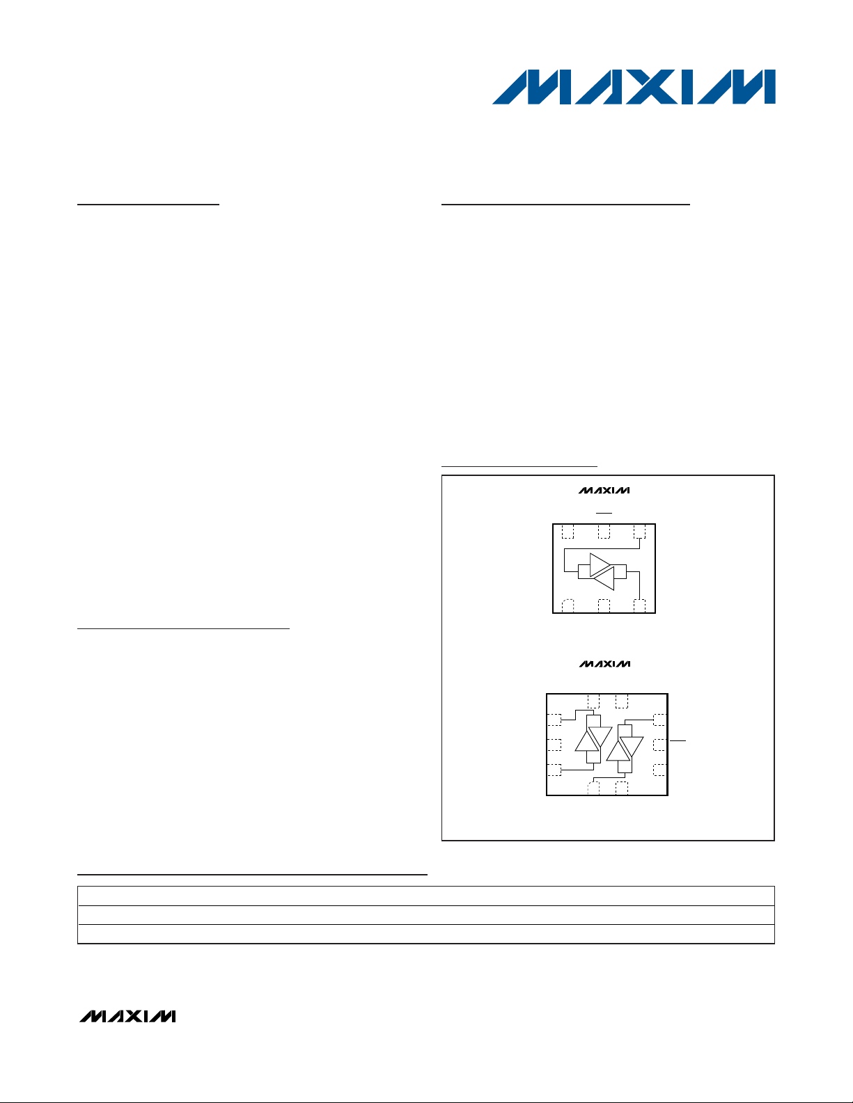
Pin Configurations
TOP VIEW
MAX13046E
µDFN
1mm × 1.5mm
2
5
SHDN
GND
1
6
V
CC
V
L1
3
4
I/O V
CC
I/O V
L
+
UTQFN
1.4mm × 1.8mm
MAX13047E
+
V
CC
N.C.
I/O V
L2VL
1 2
7
6
3
N.C.
4
SHDN
I/O V
CC2
I/O V
L1
GND
I/O V
CC1
5
10
9
8
Typical Application Circuits appear at end of data sheet.
1-Wire is a registered trademark of Maxim Integrated Products, Inc.
Page 2
MAX13046E/MAX13047E
Single- and Dual-Bidirectional
Low-Level Translator
2 _______________________________________________________________________________________
ABSOLUTE MAXIMUM RATINGS
ELECTRICAL CHARACTERISTICS
(VCC= +1.65V to +5.5V, VL= +1.1V to minimum of either +3.6V or ((VCC+ 0.3V)), I/O VL and I/O VCCare unconnected, TA= -40°C to
+85°C, unless otherwise noted. Typical values are V
CC
= +3.3V, VL= +1.8V at TA= +25°C.) (Notes 2, 3)
Stresses beyond those listed under “Absolute Maximum Ratings” may cause permanent damage to the device. These are stress ratings only, and functional
operation of the device at these or any other conditions beyond those indicated in the operational sections of the specifications is not implied. Exposure to
absolute maximum rating conditions for extended periods may affect device reliability.
(All voltages referenced to GND.)
V
CC
...........................................................................-0.3V to +6V
V
L
..............................................................................-0.3V to +4V
I/O V
CC
.......................................................-0.3V to (VCC+ 0.3V)
I/O V
L
............................................................-0.3V to (VL+ 0.3V)
SHDN........................................................................-0.3V to +6V
Short-Circuit Duration I/O V
L
, I/O VCCto GND...........Continuous
Power Dissipation (T
A
= +70°C)
6-Pin µDFN (derate 2.1mW/°C above +70°C) .............168mW
10-Pin UTQFN (derate 6.9mW/°C above +70°C).........559mW
Junction-to-Ambient Thermal Resistance (
θ
JA
) (Note 1)
6-Pin µDFN.................................................................477°C/W
10-Pin UTQFN ...........................................................20.1°C/W
Junction-to-Ambient Thermal Resistance (
θ
JC
) (Note 1)
6-Pin µDFN................................................................20.1°C/W
10-Pin UTQFN .........................................................143.1°C/W
Operating Temperature Range ...........................-40°C to +85°C
Junction Temperature......................................................+150°C
Storage Temperature Range .............................-65°C to +150°C
Lead Temperature (soldering, 10s) .................................+300°C
PARAMETER
CONDITIONS
POWER SUPPLY
VCC > 3.3V 1.1
VL Supply Range V
L
VCC ≤ 3.3V 1.1
V
VCC Supply Range V
CC
5.5 V
Supply Current from V
CC
I
QVCC
10 µA
Supply Current from V
L
I
QVL
15 µA
VCC Shutdown-Mode Supply Current I
SD-VCCTA
= +25°C, SHDN = GND
1µA
VL Shutdown-Mode Supply Current I
SD-VL
TA = +25°C, SHDN = GND
1µA
I/O VL and I/O VCC Shutdown-Mode
Leakage Current
I
SD-LKGTA
= +25°C, SHDN = GND
0.5 µA
SHDN Input Leakage TA = +25°C
0.1 µA
ESD PROTECTION
Human Body Model
IEC 61000-4-2 Air-Gap Discharge
I/O VCC (Note 4)
IEC 61000-4-2 Contact Discharge
kV
All Other Pins Human Body Model ±2 kV
LOGIC-LEVEL THRESHOLDS
I/O VL Input-Voltage High V
IHL
VL -
0.2
V
I/O VL Input-Voltage Low V
ILL
V
Note 1: Package thermal resistances were obtained using the method described in JEDEC specification JESD51-7, using a four-layer
board. For detailed information on package thermal considerations, refer to www.maxim-ic.com/thermal-tutorial
.
SYMBOL
MIN TYP MAX UNITS
V
1.65
0.03
0.03
0.02
0.02
±15V
±15V
±8V
CC
3.6V
+ 0.3V
0.15
Page 3
MAX13046E/MAX13047E
Single- and Dual-Bidirectional
Low-Level Translator
_______________________________________________________________________________________ 3
ELECTRICAL CHARACTERISTICS (continued)
(VCC= +1.65V to +5.5V, VL= +1.1V to minimum of either +3.6V or ((VCC+ 0.3V)), I/O VL and I/O VCCare unconnected, TA= -40°C to
+85°C, unless otherwise noted. Typical values are V
CC
= +3.3V, VL= +1.8V at TA= +25°C.) (Notes 2, 3)
PARAMETER
CONDITIONS
I/O VCC Input-Voltage High V
IHC
VCC -
0.4
V
I/O VCC Input-Voltage Low V
ILC
V
I/O VL Output-Voltage High V
OHL
I/O VL source current = 20µA,
V
I/O VCC
> VCC - 0.4V
0.67 x
V
L
V
I/O VL Output-Voltage Low V
OLL
I/O VL sink current = 1mA,
V
I/O VCC
< 0.15V
0.4 V
I/O VCC Output-Voltage High V
OHC
I/O VCC source current = 20µA,
V
I/O VL
> VL - 0.2V
0.67 x
V
I/O VCC Output-Voltage Low V
OLC
I/O VCC sink current = 1mA,
V
I/O VL
< 0.15V
0.4 V
VL > 1.2 VL - 0.2
SHDN Input-Voltage High
1.1 ≤ VL < 1.2 VL - 0.1
V
SHDN Input-Voltage Low
V
I/O VL-to-I/O V
CC
Resistance 80
Ω
V
CC
Shutdown Threshold Low
V
CC
falling, VL = +3.3V 0.5 0.8 1.1 V
V
CC
Shutdown Threshold High
V
CC
rising, VL = +3.3V 0.3 0.6 0.9 V
VL Shutdown Threshold V
TH_VL
V
Pullup Resistance V
CC
= VL = +3.3V 6 10
kΩ
RISE/FALL-TIME ACCELERATOR STAGE
Accelerator Pulse Duration 20 ns
I/O VL Output-Accelerator Source
Impedance
V
L
= 1.7V 13 Ω
I/O VCC Output-Accelerator Source
Impedance
V
CC
= 2.2V 17 Ω
I/O VL Output-Accelerator Source
Impedance
V
L
= 3.2V 6 Ω
I/O VCC Output-Accelerator Source
Impedance
V
CC
= 3.6V 10 Ω
SYMBOL
V
IH-SHDN
V
IL-SHDN
V
TH_L_VCC
V
TH_H_VCC
MIN TYP MAX UNITS
V
CC
0.35 0.75 1.06
0.15
0.15
250
15.5
Page 4
MAX13046E/MAX13047E
Single- and Dual-Bidirectional
Low-Level Translator
4 _______________________________________________________________________________________
TIMING CHARACTERISTICS FOR +1.2V ≤ VL≤ MINIMUM OF EITHER +3.6V OR (V
CC
+ 0.3V)
(VCC≤ ±5.5V, +1.2V ≤ VL≤ minimum of either +3.6V or ((VCC+ 0.3V)), RS= 50Ω, RL= 1MΩ, CL= 15pF, TA= -40°C to +85°C, unless
otherwise noted. Typical values are V
CC
= +3.3V, VL= +1.8V at TA= +25°C.) (Notes 2, 3, 5)
PARAMETER
CONDITIONS
Push-pull driving, Figure 1a 7 25
I/O VCC Rise Time t
RVCC
Open-drain driving, Figure 1c
ns
Push-pull driving, Figure 1a 6 37
I/O VCC Fall Time t
FVCC
Open-drain driving, Figure 1c 20 50
ns
Push-pull driving, Figure 1b 8 30
I/O VL Rise Time t
RVL
Open-drain driving, Figure 1d
ns
Push-pull driving, Figure 1 3 56
I/O VL Fall Time t
FVL
Open-drain driving, Figure 1d 30 60
ns
Push-pull driving 5 30
Driving I/O V
L
Push-pull driving 4 30
Propagation Delay
Driving I/O V
CC
ns
Push-pull driving 20
Channel-to-Channel Skew t
SKEW
Each translator
equally loaded
50
ns
Push-pull driving 8
Maximum Data Rate
Open-drain driving
TIMING CHARACTERISTICS FOR +1.1V ≤ VL≤ +1.2V
(VCC≤ ±5.5V, +1.1V ≤ VL≤ +1.2V, RS= 50Ω, RL= 1MΩ, CL= 15pF, TA= -40°C to +85°C, unless otherwise noted. Typical values are
V
CC
= +3.3V, VL= +1.8V at TA= +25°C.) (Notes 2, 3, 5)
PARAMETER
CONDITIONS
Push-pull driving, Figure 1a 7
I/O VCC Rise Time t
RVCC
Open-drain driving, Figure 1c
ns
Push-pull driving, Figure 1a 6 37
I/O VCC Fall Time t
FVCC
Open-drain driving, Figure 1c 20 50
ns
Push-pull driving, Figure 1b 8 30
I/O VL Rise Time t
RVL
Open-drain driving, Figure 1d
ns
Push-pull driving, Figure 1 3 30
I/O VL Fall Time t
FVL
Open-drain driving, Figure 1d 30 60
ns
Push-pull driving 5
Driving I/O V
L
Push-pull driving 4
Propagation Delay
Driving I/O V
CC
ns
Push-pull driving 20
Channel-to-Channel Skew t
SKEW
Each translator
equally loaded
50
ns
Push-pull driving 1.2
Maximum Data Rate
Open-drain driving
SYMBOL
t
PD-VL-VCC
t
PD-VCC-VL
Open-drain driving 210 1000
Open-drain driving 190 1000
Open-drain driving
MIN TYP MAX UNITS
170 400
180 400
500 kbps
Mbps
SYMBOL
t
PD-VL-VCC
t
PD-VCC-VL
Open-drain driving 210 1000
Open-drain driving 190 1000
Open-drain driving
MIN TYP MAX UNITS
500 kbps
200
170 400
180 400
200
200
Mbps
Page 5
MAX13046E/MAX13047E
Single- and Dual-Bidirectional
Low-Level Translator
_______________________________________________________________________________________ 5
TIMING CHARACTERISTICS FOR +1.8V ≤ VL≤ VCC≤ +3.3V
(+1.8V ≤ VL≤ VCC≤ +3.3V, RS= 50Ω, RL= 1MΩ, CL= 15pF, TA= -40°C to +85°C, unless otherwise noted. Typical values are VCC= +3.3V,
V
L
= +1.8V at TA= +25°C.) (Notes 2, 3, 5)
PARAMETER
CONDITIONS
I/O VCC Rise Time t
RVCC
Push-pull driving, Figure 1a 15 ns
I/O VCC Fall Time t
FVCC
Push-pull driving, Figure 1a 15 ns
I/O VL Rise Time t
RVL
Push-pull driving, Figure 1b 15 ns
I/O VL Fall Time t
FVL
Push-pull driving, Figure 1b 15 ns
Push-pull driving, driving I/O V
L
15
Propagation Delay
Push-pull driving, driving I/O V
CC
15
ns
Channel-to-Channel Skew t
SKEW
Push-pull driving, each translator
equally loaded
10 ns
Maximum Data Rate Push-pull driving 16
Note 2: All units are 100% production tested at TA= +25°C. Limits over the operating temperature range are guaranteed by design
and not production tested.
Note 3: For normal operation, ensure V
L
< (VCC+ 0.3V). During power-up, VL> (VCC+ 0.3V) does not damage the device.
Note 4: ESD protection is guaranteed by design. To ensure maximum ESD protection, place a 1µF ceramic capacitor between V
CC
and GND. See
Typical Application Circuits
.
Note 5: Timing is measured using 10% of input to 90% of output.
SYMBOL
t
PD-VL-VCC
t
PD-VCC-VL
MIN TYP MAX UNITS
Mbps
Page 6

MAX13046E/MAX13047E
Single- and Dual-Bidirectional
Low-Level Translator
6 _______________________________________________________________________________________
Typical Operating Characteristics
(VCC= +3.3V, VL= +1.8V, RL= 1MΩ, CL= 15pF, push-pull driving data rate = 8Mbps, TA= +25°C, unless otherwise noted.)
VL DYNAMIC SUPPLY CURRENT
vs. V
CC
SUPPLY VOLTAGE
(PUSH-PULL DRIVING ONE I/O V
L
)
VCC SUPPLY VOLTAGE (V)
V
L
SUPPLY CURRENT (μA)
MAX13046E/7E toc01
1.65 2.20 2.75 3.30 3.85 4.40 4.95 5.50
0
50
100
150
200
250
300
350
VL DYNAMIC SUPPLY CURRENT
vs. V
CC
SUPPLY VOLTAGE
(PUSH-PULL DRIVING ONE I/O V
CC
)
VCC SUPPLY VOLTAGE (V)
V
L
SUPPLY CURRENT (μA)
MAX13046E/7E toc02
1.65 2.20 2.75 3.30 3.85 4.40 4.95 5.50
0
50
100
150
200
250
VCC DYNAMIC SUPPLY CURRENT
vs. V
L
SUPPLY VOLTAGE
(PUSH-PULL DRIVING ONE I/O V
L
)
VL SUPPLY VOLTAGE (V)
V
CC
SUPPLY CURRENT (μA)
MAX13046E/7E toc03
1.2 1.9 2.6 3.3
0
100
200
300
400
500
600
VCC DYNAMIC SUPPLY CURRENT
vs. V
L
SUPPLY VOLTAGE
(PUSH-PULL DRIVING ONE I/O V
CC
)
VL SUPPLY VOLTAGE (V)
V
CC
SUPPLY CURRENT (μA)
MAX13046E/7E toc04
1.2 1.9 2.6 3.3
0
10
20
30
40
50
60
70
80
VL DYNAMIC SUPPLY CURRENT
vs. TEMPERATURE
(PUSH-PULL DRIVING ONE I/O V
L
)
TEMPERATURE (°C)
V
L
SUPPLY CURRENT (μA)
MAX13046E/7E toc05
-40 -15 10 35 60 85
0
20
40
60
80
100
120
140
160
180
200
VL DYNAMIC SUPPLY CURRENT
vs. TEMPERATURE
(PUSH-PULL DRIVING ONE I/O V
CC
)
TEMPERATURE (°C)
V
L
SUPPLY CURRENT (μA)
MAX13046E/7E toc06
-40 -15 10 35 60 85
0
50
100
150
200
250
300
350
VL DYNAMIC SUPPLY CURRENT
vs. CAPACITIVE LOAD
(PUSH-PULL DRIVING ONE I/O V
L
)
CAPACITIVE LOAD (pF)
V
L
SUPPLY CURRENT (μA)
MAX13046E/7E toc07
0 1020304050
0
20
40
60
80
100
120
VCC DYNAMIC SUPPLY CURRENT
vs. CAPACITIVE LOAD
(PUSH-PULL DRIVING ONE I/O V
L
)
CAPACITIVE LOAD (pF)
V
CC
SUPPLY CURRENT (μA)
MAX13046E/7E toc08
0 1020304050
0
200
400
600
800
1000
1200
RISE/FALL TIME vs. CAPACITIVE LOAD
(PUSH-PULL DRIVING ONE I/O V
L
)
CAPACITIVE LOAD (pF)
RISE/FALL TIME (ns)
MAX13046E/7E toc09
0 1020304050
0
5
10
15
20
25
t
FVCC
t
RVCC
Page 7

MAX13046E/MAX13047E
Single- and Dual-Bidirectional
Low-Level Translator
_______________________________________________________________________________________ 7
Typical Operating Characteristics (continued)
(VCC= +3.3V, VL= +1.8V, RL= 1MΩ, CL= 15pF, push-pull driving data rate = 8Mbps, TA= +25°C, unless otherwise noted.)
PROPAGATION DELAY vs. CAPACITIVE LOAD
(PUSH-PULL DRIVING ONE I/O V
L
)
CAPACITIVE LOAD (pF)
PROPAGATION DELAY (ns)
MAX13046E/7E toc10
0 1020304050
0
1
2
3
4
5
6
7
RISE/FALL TIME vs. CAPACITIVE LOAD
(PUSH-PULL DRIVING ONE I/O V
CC
)
CAPACITIVE LOAD (pF)
RISE/FALL TIME (ns)
MAX13046E/7E toc11
0 1020304050
0
2
4
6
8
10
12
t
RVL
t
FVL
PROPAGATION DELAY vs. CAPACITIVE LOAD
(PUSH-PULL DRIVING ONE I/O V
CC
)
CAPACITIVE LOAD (pF)
PROPAGATION DELAY (ns)
MAX13046E/7E toc12
0 1020304050
0
0.5
1.0
1.5
2.0
2.5
3.0
3.5
RAIL-TO-RAIL DRIVING
(DRIVING ONE I/O V
L
)
MAX13046E/7E toc13
25ns/div
I/O V
L
I/O V
CC
1V/div
1V/div
EXISTING SHUTDOWN MODE
MAX13046E/7E toc14
250ns/div
I/O V
L
I/O V
CC
1V/div
2V/div
1V/div
SHDN
Page 8

MAX13046E/MAX13047E
Detailed Description
The MAX13046E/MAX13047E ±15kV ESD-protected
bidirectional level translators provide level shifting for
data transfer in a multivoltage system. The MAX13046E
is a single-channel translator and the MAX13047E is a
dual-channel translator. Externally applied voltages,
VCCand VL, set the logic level on either side of the
device. The MAX13046E/MAX13047E utilize a transmission-gate-based design to allow data translation in
either direction (VL↔ VCC) on any single data line. The
MAX13046E/MAX13047E accept VLfrom +1.1V to the
minimum of either +3.6V or (V
CC
+ 0.3V) and VCCfrom
+1.65V to +5.5V, making these devices ideal for data
transfer between low-voltage ASICs/PLDs and higher
voltage systems.
The MAX13046E/MAX13047E feature a shutdown mode
that reduces supply current to less than 1µA thermal
short-circuit protection, and ±15kV ESD protection on the
VCCside for enhanced protection in applications that
route signals externally. The MAX13046E/MAX13047E
operate at a guaranteed data rate of 8Mbps when pushpull driving is used. See the
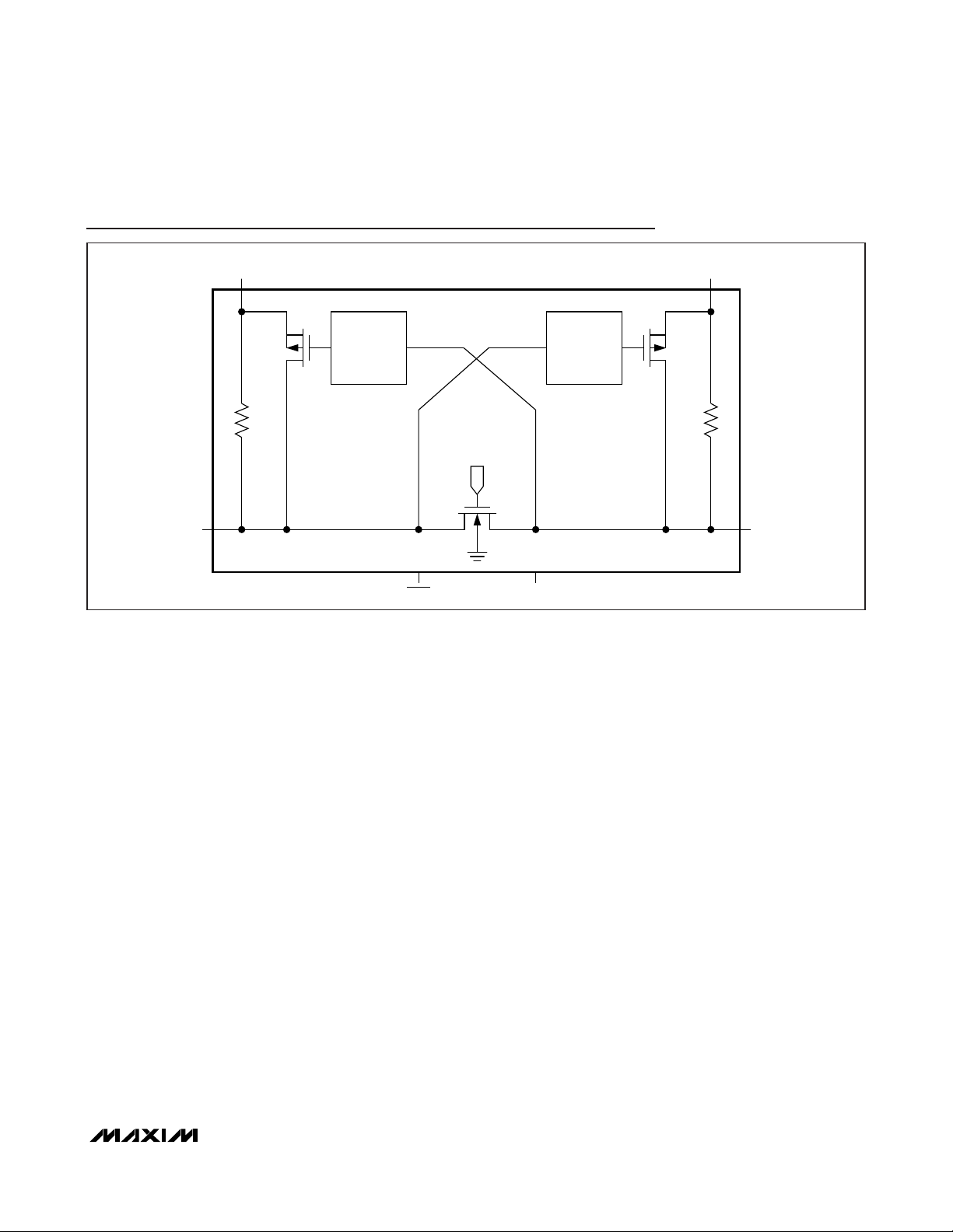
Functional Diagram
.
Single- and Dual-Bidirectional
Low-Level Translator
8 _______________________________________________________________________________________
MAX13046E Pin Description
MAX13046E FUNCTION
µDFN
1VLV L Inp ut S up p l y V ol tag e. Byp ass V L w i th a 0.1µF cer am i c cap aci tor l ocated as cl ose as p ossi b l e to the i np ut.
2 GND Ground
3 I/O VLInput/Output. Referenced to VL.
4
Input/Output. Referenced to VCC.
5 SHDN S hutd ow n Inp ut. D r i ve S HD N hi g h to enab l e the d evi ce. D r i ve S HD N l ow to p ut the d evi ce i n shutd ow n m od e.
6V
CC
V CC Inp ut S up p l y V ol tag e. Byp ass V CC w i th a 1µF cer am i c cap aci tor l ocated as cl ose as p ossi b l e to the i np ut
for ful l E S D p r otecti on. If ful l E S D p r otecti on i s not r eq ui r ed , b yp ass V
CC
w i th a 0.1µF cer am i c cap aci tor .
MAX13047E Pin Description
MAX13047E FUNCTION
1
Input/Output 2. Referenced to VL.
2V
L
VL Input Supply Voltage. Bypass VL with a 0.1µF ceramic capacitor located as close as possible to the
input.
3, 7 N.C. Not Connected. Internally not connected.
4 SHDN Enable Input. Drive SHDN high to enable the device. Drive SHDN low to put the device in shutdown mode.
5
Input/Output 2. Referenced to VCC.
6V
CC
VCC Input Supply Voltage. Bypass VCC with a 1µF ceramic capacitor located as close as possible to the
input for full ESD protection. If full ESD protection is not required, bypass V
CC
with a 0.1µF ceramic
capacitor.
8
Input/Output 1. Referenced to VCC.
9 GND Ground
10
Input/Output 1. Referenced to VL.
— EP Exposed Pad. Connect EP to GND.
NAME
I/O V
CC
UTQFN NAME
I/O V
L2
I/O V
CC2
I/O V
CC1
I/O V
L1
Page 9
Level Translation
For proper operation, ensure that +1.65V ≤ VCC≤
+5.5V and +1.1V ≤ VL≤ the minimum of either +3.6V or
(V
CC
+ 0.3V). During power-up sequencing, VL≥ (V
CC
+ 0.3V) does not damage the device. The speed of the
rise time accelerator circuitry limits the maximum data
rate for the MAX13046E/MAX13047E to 16Mbps.
Rise-Time Accelerators
The MAX13046E/MAX13047E have an internal rise-time
accelerator, allowing operation up to 16Mbps. The risetime accelerators are present on both sides of the
device and act to speed up the rise time of the input
and output of the device, regardless of the direction of
the data. The triggering mechanism for these accelerators is both level and edge sensitive. To guarantee
operation of the rise time accelerators the maximum
parasitic capacitance should be less than 200pF on the
I/O lines.
Shutdown Mode
Drive SHDN low to place the MAX13046E/MAX13047E
in shutdown mode and drive SHDN high for normal
operation. Activating the shutdown mode disconnects
the internal 10kΩ pullup resistors on the I/O VCCand I/O
VLlines. This forces the I/O lines to a high-impedance
state, and decreases the supply current to less than
1µA. The high-impedance I/O lines in shutdown mode
allow for use in a multidrop network. The MAX13046E/
MAX13047E have a diode from each I/O to the corresponding supply rail and GND. Therefore, when in shutdown mode, do not allow the voltage at I/O VLto exceed
(VL + 0.3V), or the voltage at I/O V
CC
to exceed (V
CC
+
0.3V).
Operation with One Supply Disconnected
Certain applications require sections of circuitry to be
disconnected to save power. When VLis connected and
VCCis disconnected or connected to ground, the device
enters shutdown mode. In this mode, I/O VLcan still be
driven without damage to the device; however, data
does not translate from I/O VLto I/O VCC. If VCCfalls
more than V
TH_L_VCC
below VL, the device disconnects
the pullup resistors at I/O VLand I/O VCC. To achieve the
lowest possible supply current from VLwhen VCCis disconnected, it is recommended that the voltage at the
VCCsupply input be approximately equal to GND.
When VCCis connected and VLis less than V
TH_VL
, the
device enters shutdown mode. In this mode, I/O V
CC
can still be driven without damage to the device; however, data does not translate from I/O VCCto I/O VL.
MAX13046E/MAX13047E
Single- and Dual-Bidirectional
Low-Level Translator
_______________________________________________________________________________________ 9
ONE-SHOT
RISE-TIME
ACCELERATOR
V
L
SHDN
I/O V
L
I/O V
CC
V
CC
GATE BIAS
ONE-SHOT
RISE-TIME
ACCELERATOR
PU2PU1
N
10kΩ 10kΩ
GND
Functional Diagram
Page 10

MAX13046E/MAX13047E
When VCCis disconnected or connected to ground, I/O
VCCmust not be driven more than VCC+ 0.3V. When V
L
is disconnected or connected to ground, I/O VLmust
not be driven more than VL+ 0.3V.
Short-Circuit Protection
Thermal-overload detection protects the MAX13046E/
MAX13047E from short-circuit fault conditions. In the
event of a short-circuit fault, when the junction temperature (T
J
) exceeds +150°C, the device enters shutdown
mode. When the device has cooled to below +140°C,
normal operation resumes.
±15kV ESD Protection
ESD protection structures are incorporated on all pins
to protect against electrostatic discharges encountered
during handling and assembly. The ESD structures
withstand electrostatic discharge in all states: normal
operation, shutdown mode, and powered down. The
I/O VCClines of the MAX13046E/MAX13047E are characterized for protection to the following limit:
• ±15kV using the Human Body Model
ESD Test Conditions
ESD performance depends on a variety of conditions.
Contact Maxim for a reliability report that documents
test setup, test methodology, and test results.
Human Body Model
Figure 2a shows the Human Body Model, and Figure
2b shows the current waveform it generates when discharged into a low-impedance state. This model consists of a 100pF capacitor charged to the ESD voltage
of interest that is then discharged into the test device
through a 1.5kΩ resistor.
Single- and Dual-Bidirectional
Low-Level Translator
10 ______________________________________________________________________________________
MAX13046E/
MAX13047E
I/O V
L
I/O V
CC
(t
RISE
,
t
FALL
< 10ns)
DATA
I/O V
CC
V
CC
V
CC
V
L
GND
R
L
C
L
t
PD-VCC-VL
t
PD-VCC-VL
I/O V
L
t
RVL
t
FVL
SHDN
V
L
R
S
50Ω
MAX13046E/
MAX13047E
I/O V
L
I/O V
L
(t
RISE
,
t
FALL
< 10ns)
DATA
I/O V
CC
R
L
C
L
V
CC
V
CC
V
L
GND
t
PD-VL-VCC
t
PD-VL-VCC
I/O V
CC
t
RVCC
t
FVCC
SHDN
V
L
R
S
50Ω
Figure 1a. Rail-to-Rail Driving I/O V
L
Figure 1b. Rail-to-Rail Driving I/O V
CC
Page 11

IEC 61000-4-2
The IEC 61000-4-2 standard covers ESD testing and performance of finished equipment; it does not specifically
refer to integrated circuits. The MAX13046E/MAX13047E
help to design equipment that meets Level 4 of IEC
61000-4-2 without the need for additional ESD-protection
components. The major difference between tests done
using the Human Body Model and IEC 61000-4-2 is higher peak current in IEC 61000-4-2 because series resistance is lower in the IEC 61000-4-2 model. Hence, the
ESD withstand voltage measured to IEC 61000-4-2 can
be lower than that measured using the Human Body
Model. Figure 3a shows the IEC 61000-4-2 model, and
Figure 3b shows the current waveform for the ±8kV, IEC
61000-4-2, Level 4, ESD contact-discharge test. The AirGap test involves approaching the device with a charged
probe. The contact-discharge method connects the
probe to the device before the probe is energized.
Applications Information
Power-Supply Decoupling
To reduce ripple and the chance of transmitting incorrect data, bypass VLand VCCto ground with a 0.1µF
ceramic capacitor
.
To ensure full ±15kV ESD protection, bypass VCCto ground with a 1µF ceramic capacitor. Place all capacitors as close as possible to the
power-supply inputs.
I2C Level Translation
The MAX13046E/MAX13047E level shifts the data present on the I/O lines between +1.1V and +5.5V, making
them ideal for level translation between a low-voltage
ASIC and an I2C device. A typical application involves
interfacing a low-voltage microprocessor to a +3V or
+5V D/A converter, such as the MAX517.
1-Wire Interface Translation
The MAX13046E/MAX13047E are ideal for level translation between a low-voltage ASIC and 1-Wire device. A
MAX13046E/MAX13047E
Single- and Dual-Bidirectional
Low-Level Translator
______________________________________________________________________________________ 11
MAX13046E/
MAX13047E
I/O V
L
I/O V
CC
DATA
I/O V
CC
V
CC
V
CC
V
L
GND
R
L
C
L
t
PD-VCC-VL
t
PD-VCC-VL
I/O V
L
t
RVL
t
FVL
SHDN
V
L
MAX13046E/
MAX13047E
I/O V
L
I/O V
CC
V
CC
V
CC
V
L
GND
I/O V
CC
t
PD-VL-VCC
t
PD-VL-VCC
I/O V
L
t
RVCC
t
FVCC
DATA
R
L
C
L
SHDN
V
L
Figure 1c. Open-Drain Driving I/O V
L
Figure 1d. Open-Drain Driving I/O V
CC
Page 12

MAX13046E/MAX13047E
typical application involves interfacing a low-voltage
microprocessor to an external memory, such as the
DS2502. The maximum data rate depends on the
1-Wire device. For the DS2502, the maximum data rate
is 16.3kbps. A 5kΩ pullup resistor is recommended
when interfacing with the DS2502.
Push-Pull vs. Open-Drain Driving
The MAX13046E/MAX13047E can be driven in a pushpull or open-drain configurations. For open-drain configuration, internal 10kΩ resistors pull up I/O V
L
and I/O
V
CC
to their respective power supplies. See the
Timing
Characteristics
table for maximum data rates when
using open-drain drivers.
PCB Layout
The MAX13046E/MAX13047E require good PCB layout
for proper operation and optimal rise/fall time performance. Ensure proper high-frequency PCB layout even
when operating at low data rates.
Driving High-Capacitive Load
Capacitive loading on the I/O lines impacts the rise time
(and fall time) of the MAX13046E/MAX13047E when driving the signal lines. The actual rise time is a function of
the load capacitance, parasitic capacitance, the supply
voltage, and the drive impedance of the MAX13046E/
MAX13047E.
Operating the MAX13046E/MAX13047E at a low data rate
does NOT increase capacitive load driving capability.
Single- and Dual-Bidirectional
Low-Level Translator
12 ______________________________________________________________________________________
IP 100%
90%
36.8%
t
RL
TIME
t
DL
CURRENT WAVEFORM
PEAK-TO-PEAK RINGING
(NOT DRAWN TO SCALE)
I
r
10%
0
0
AMPERES
Figure 2b. Human Body Current Waveform
CHARGE-CURRENT-
LIMIT RESISTOR
DISCHARGE
RESISTANCE
STORAGE
CAPACITOR
C
s
100pF
R
C
1MΩ
R
D
1500Ω
HIGH-
VOLTAGE
DC
SOURCE
DEVICE
UNDER
TEST
Figure 2a. Human Body ESD Test Model
100%
90%
60ns
10%
tr = 0.7ns TO 1ns
I
PEAK
I
30ns
t
Figure 3b. IEC 61000-4-2 ESD Generator Current Waveform
CHARGE-CURRENT-
LIMIT RESISTOR
DISCHARGE
RESISTANCE
STORAGE
CAPACITOR
C
s
150pF
R
C
50MΩ TO 100MΩ
R
D
330Ω
HIGH-
VOLTAGE
DC
SOURCE
DEVICE
UNDER
TEST
Figure 3a. IEC 61000-4-2 ESD Test Model
Page 13

MAX13046E/MAX13047E
Single- and Dual-Bidirectional
Low-Level Translator
______________________________________________________________________________________ 13
MAX13046E
SHDN
I/O V
L
DATADATA
I/O V
CC
0.1μF 1μF
+3.3V+1.8V
V
CC
+3.3V
SYSTEM
+1.8V
SYSTEM
V
L
Typical Application Circuits
MAX13047E
SHDN
I/O V
L2
DATADATA
I/O V
CC2
0.1μF 1μF
+3.3V+1.8V
V
CC
+3.3V
SYSTEM
+1.8V
SYSTEM
V
L
I/O V
L1
I/O V
CC1
Page 14

MAX13046E/MAX13047E
Single- and Dual-Bidirectional
Low-Level Translator
14 ______________________________________________________________________________________
Chip Information
PROCESS: BiCMOS
Package Information
For the latest package outline information and land patterns, go
to www.maxim-ic.com/packages
.
PACKAGE TYPE PACKAGE CODE DOCUMENT NO.
6 µDFN L611-1
21-0147
10 UTQFN V101A1CN-1
21-0028
Page 15

MAX13046E/MAX13047E
Single- and Dual-Bidirectional
Low-Level Translator
Maxim cannot assume responsibility for use of any circuitry other than circuitry entirely embodied in a Maxim product. No circuit patent licenses are
implied. Maxim reserves the right to change the circuitry and specifications without notice at any time.
Maxim Integrated Products, 120 San Gabriel Drive, Sunnyvale, CA 94086 408-737-7600 ____________________
15
© 2008 Maxim Integrated Products is a registered trademark of Maxim Integrated Products, Inc.
Revision History
REVISION
NUMBER
REVISION
DATE
DESCRIPTION
PAGES
CHANGED
0 5/08 Initial release ⎯
18/08
Removing future product asterisks from MAX13047, changing Electrical
Characteristics Table, packaging changes, changing ESD information
1–4, 6, 10
 Loading...