

General Description
The MAX13042E–MAX13045E 4-channel, bidirectional
level translators provide the level shifting necessary for
100Mbps data transfer in multivoltage systems. The
MAX13042E–MAX13045E are ideally suited for level
translation in systems with four channels. Externally
applied voltages, VCCand VL, set the logic levels on
either side of the device. Logic signals present on the
VLside of the device appear as a high-voltage logic
signal on the VCCside of the device and vice-versa.
The MAX13042E–MAX13045E operate at full speed
with external drivers that source as little as 4mA output
current or larger. Each input/output (I/O) channel is
pulled up to V
CC
or VLby an internal 30µA current
source, allowing the MAX13042E–MAX13045E to be
driven by either push-pull or open-drain drivers.
The MAX13042E–MAX13045E feature an enable (EN)
input that places the devices into a low-power shutdown
mode when driven low. The MAX13042E–MAX13045E
feature an automatic shutdown mode that disables the
part when VCCis less than VL. The state of I/O V
CC_
and
I/O VL_during shutdown is chosen by selecting the
appropriate part version. (See the Ordering Information/
Selector Guide).
The MAX13042E–MAX13045E operate with VCCvoltages from +2.2V to +3.6V and VLvoltages from +1.62V
to +3.2V, making them ideal for data transfer between
low-voltage ASIC/PLDs and higher voltage systems.
The MAX13042E–MAX13045E are available in 12-bump
UCSP™ (1.54mm x 2.12mm) and 14-pin TDFN (3mm x
3mm) packages, and operate over the extended -40°C
to +85°C temperature range.
Applications
Features
♦ Compatible with 4mA Input Drivers or Larger
♦ 100Mbps Guaranteed Data Rate
♦ Four Bidirectional Channels
♦ Enable Input
♦ ±15kV ESD Protection on I/O V
CC_
Lines
♦ +1.62V ≤ VL≤ +3.2V and +2.2V ≤ VCC≤ +3.6V
Supply Voltage Range
♦ 12-Bump UCSP (1.54mm x 2.12mm) and
14-Pin TDFN (3mm x 3mm) Lead-Free Packages
MAX13042E–MAX13045E
1.62V to 3.6V Improved High-Speed LLT
________________________________________________________________ Maxim Integrated Products 1
19-0792; Rev 0; 4/07
For pricing, delivery, and ordering information, please contact Maxim/Dallas Direct! at
1-888-629-4642, or visit Maxim’s website at www.maxim-ic.com.
Ordering Information/Selector Guide
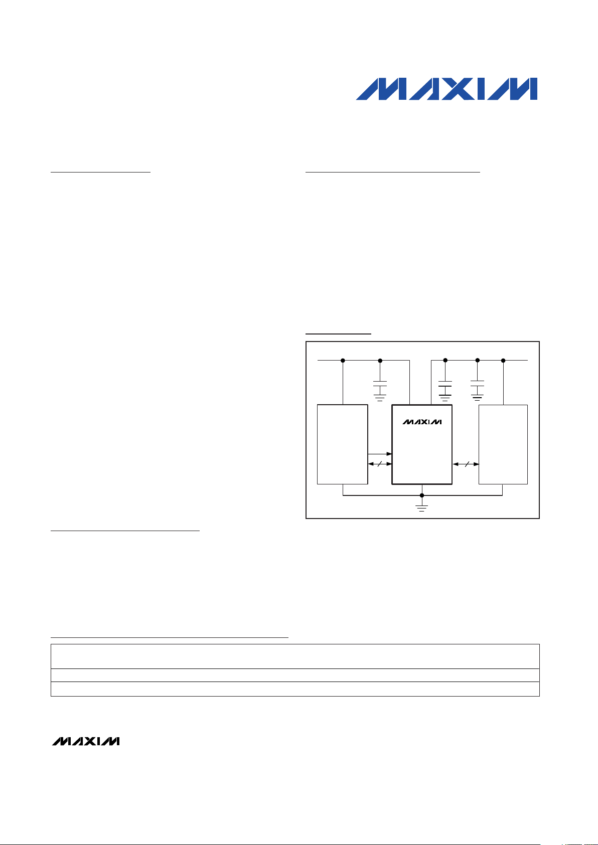
GND GND GND
+1.8V
SYSTEM
CONTROLLER
+3.3V
SYSTEM
V
L
V
CC
I/O V
L_
I/O V
CC_
DATA
DATA
+3.3V
+1.8V
EN
EN
1µF
0.1µF
0.1µF
MAX13042E–
MAX13045E
4
4
Typical Operating Circuit
PART
PINPACKAGE
I/O VL_ STATE DURING
SHUTDOWN
I/O V
CC_
STATE DURING
SHUTDOWN
TOP
MARK
PKG CODE
MAX13042EEBC+T
12 UCSP-12 High Impedance High Impedance
ADQ
B12-3
MAX13042EETD+T
14 TDFN-EP**
High Impedance High Impedance ADE T1433-2
Note: All devices operate over the -40°C to +85°C temperature
range.
+Denotes a lead-free package.
*Future product—contact factory for availability.
**EP = Exposed paddle.
Pin Configurations appear at end of data sheet.
UCSP is a trademark of Maxim Integrated Products, Inc.
SPI is a trademark of Motorola, Inc.
MICROWIRE is a trademark of National Semiconductor Corp.
Ordering Information/Selector Guide continued at end of
data sheet.
CMOS Logic-Level
Translation
Low-Voltage ASIC Level
Translation
Cell Phones
SPI™, MICROWIRE™
Level Translation
Portable POS Systems
Portable Communication
Devices
GPS
Telecommunications
Equipment
MAX13042E–MAX13045E
1.62V to 3.6V Improved High-Speed LLT
2 _______________________________________________________________________________________
ABSOLUTE MAXIMUM RATINGS
Stresses beyond those listed under “Absolute Maximum Ratings” may cause permanent damage to the device. These are stress ratings only, and functional
operation of the device at these or any other conditions beyond those indicated in the operational sections of the specifications is not implied. Exposure to
absolute maximum rating conditions for extended periods may affect device reliability.
(All voltages referenced to GND.)
V
CC
, VL.....................................................................-0.3V to +4V
I/O V
CC_
..................................................... -0.3V to (VCC+ 0.3V)
I/O V
L_
...........................................................-0.3V to (VL+ 0.3V)
EN.............................................................................-0.3V to +4V
Short-Circuit Duration I/O V
L_
, I/O V
CC_
to GND .......Continuous
Continuous Power Dissipation (T
A
= +70°C)
12-Bump UCSP (derate 6.5mW/°C above +70°C) ......519mW
14-Pin TDFN (derate 24.4mW/°C above +70°C) .......1951mW
Operating Temperature Range ...........................-40°C to +85°C
Storage Temperature Range .............................-65°C to +150°C
Junction Temperature......................................................+150°C
Lead Temperature (soldering, 10s) .................................+300°C
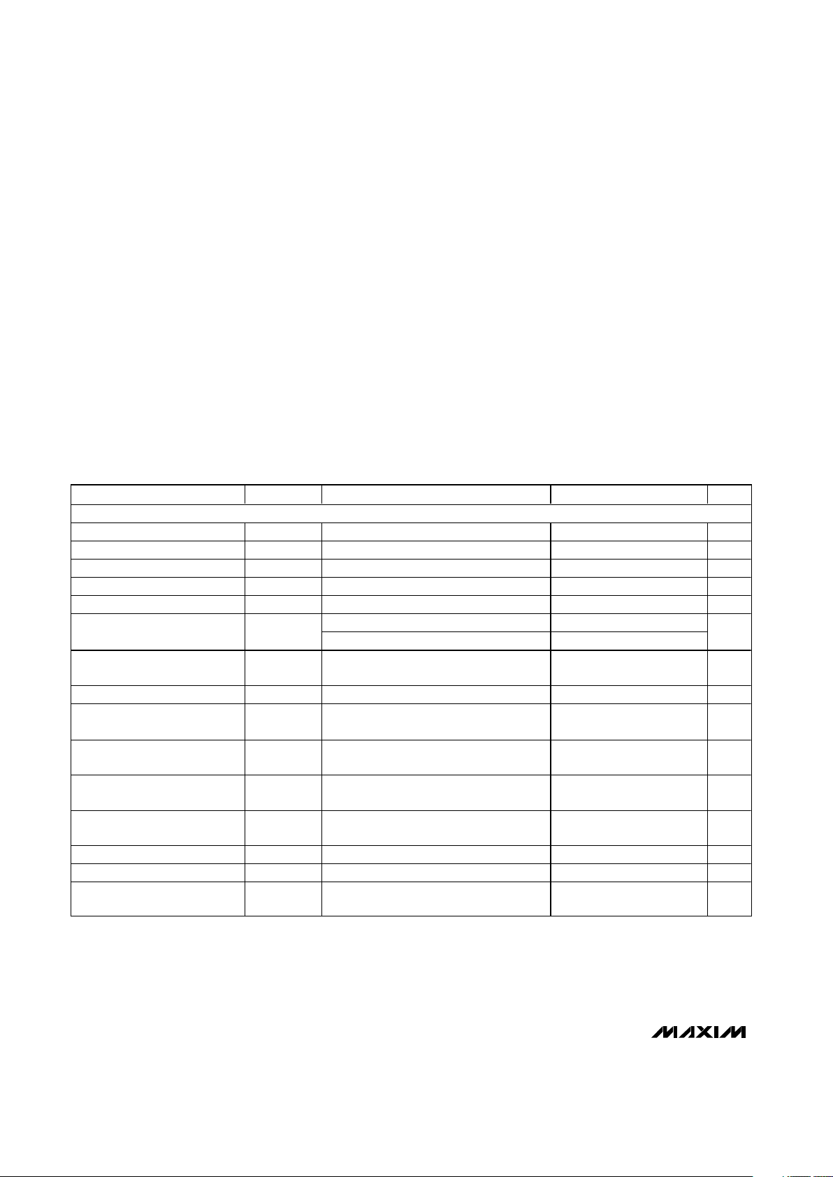
ELECTRICAL CHARACTERISTICS
(VCC= +2.2V to +3.6V, VL= +1.62V to +3.2V, EN = VL, TA= -40°C to +85°C, unless otherwise noted. Typical values are at VCC=
+3.3V, V
L
= +1.8V, and TA= +25°C.) (Notes 1, 2)
PARAMETER
SYMBOL
CONDITIONS MIN TYP
MAX
UNITS
POWER SUPPLIES
VL Supply Range V
L
1.62 3.2 V
VCC Supply Range V
CC
2.2 3.6 V
Supply Current from V
CC
I
QVCC
I/O V
CC_
= VCC, I/O VL_ = V
L
25 µA
Supply Current from V
L
I
QVL
I/O V
CC_
= VCC, I/O VL_ = V
L
10 µA
VCC Shutdown Supply Current
I
SHDN-VCC
TA = +25°C, EN = GND 0.1 1 µA
TA = +25°C, EN = GND 0.1 1
VL Shutdown-Mode Supply
Current
I
SHDN-VL
TA = +25°C, EN = VL, VCC = GND 0.1 4
µA
I/O V
CC_
, I/O VL_ Tri-State
Leakage Current
I
LEAK
TA = +25°C, EN = GND 0.1 2 µA
EN Input Leakage Current I
LEAK_ENTA
= +25°C1µA
VL - VCC Shutdown Threshold
High
V
TH_H
VCC rising (Note 3) 0
0.1V
L
0.8 V
VL - VCC Shutdown Threshold
Low
V
TH_L
VCC falling (Note 3) 0
0.12V
L
0.8 V
I/O V
CC_
Pulldown Resistance
During Shutdown
R
VCC_PD_SD
MAX13043E/MAX13045E 10 16.5 23 kΩ
I/O VL_ Pulldown Resistance
During Shutdown
R
VL_PD_SD
MAX13044E/MAX13045E 10 16.5 23 kΩ
I/O VL_ Pullup Current I
VL_PU_
I/O VL_ = GND, I/O V
CC_
= GND 20 65 µA
I/O V
CC_
Pullup Current I
VCC_PU_
I/O V
CC_
= GND, I/O V
L_
= GND 20 65 µA
I/O V
L_
to I/O V
CC_
DC
Resistance
R
IOVL_IOVCC
(Note 4) 3 kΩ
MAX13042E–MAX13045E
1.62V to 3.6V Improved High-Speed LLT
_______________________________________________________________________________________ 3
PARAMETER
SYMBOL
CONDITIONS MIN TYP
MAX
UNITS
ESD PROTECTION
I/O VL_, EN Human Body Model ±2 kV
Human Body Model, C
VCC
= 1µF ±15
IEC 61000-4-2 Air-Gap Discharge,
C
VCC
= 1µF
±15
I/O V
CC_
IEC 61000-4-2 Contact Discharge,
C
VCC
= 1µF
±8
kV
LOGIC LEVELS
I/O VL_ Input-Voltage High
Threshold
V
IHL
(Note 5)
VL - 0.2
V
I/O VL_ Input-Voltage Low
Threshold
V
ILL
(Note 5) 0.15 V
I/O V
CC_
Input-Voltage High
Threshold
V
IHC
(Note 5)
V
CC
-
0.4
V
I/O V
CC_
Input-Voltage Low
Threshold
V
ILC
(Note 5) 0.2 V
EN Input-Voltage-High
Threshold
V
IH
VL - 0.4
V
EN Input-Voltage-Low
Threshold
V
IL
0.4 V
I/O VL_ Output-Voltage High V
OHL
I/O VL_ source current = 20µA
2/3 V
L
V
I/O VL_ Output-Voltage Low V
OLL
I/O V
L _
si nk cur r ent = 20µA, I/O V
C C _
< 0.2V 1/3 V
L
V
I/O V
CC_
Output-Voltage High V
OHC
I/O V
CC_
source current = 20µA
2/3 V
CC
V
I/O V
CC_
Output-Voltage Low V
OLC
I/O V
C C _
si nk cur r ent = 20µA,
I/O V
L _
< 0.15V
1/3 V
CC
V
RISE-/FALL-TIME ACCELERATOR STAGE
On falling edge 3.5
Accelerator Pulse Duration
On rising edge 3.5
ns
VL = 1.62V 24
VL Output Accelerator Source
Impedance
V
L
= 3.2V 11
Ω
VCC = 2.2V 13
VCC Output Accelerator Source
Impedance
V
CC
= 3.6V 9
Ω
VL = 1.62V 14
VL Output Accelerator Sink
Impedance
V
L
= 3.2V 10
Ω
VCC = 2.2V 11
VCC Output Accelerator Sink
Impedance
V
CC
= 3.6V 9
Ω
ELECTRICAL CHARACTERISTICS (continued)
(VCC= +2.2V to +3.6V, VL= +1.62V to +3.2V, EN = VL, TA= -40°C to +85°C, unless otherwise noted. Typical values are at VCC=
+3.3V, V
L
= +1.8V, and TA= +25°C.) (Notes 1, 2)
MAX13042E–MAX13045E
1.62V to 3.6V Improved High-Speed LLT
4 _______________________________________________________________________________________
PARAMETER
SYMBOL
CONDITIONS
MIN TYP MAX
UNITS
I/O V
CC_
Rise Time t
RVCC
Figure 1 2.5 ns
I/O V
CC_
Fall Time t
FVCC
Figure 1 2.5 ns
I/O VL_ Rise Time t
RVL
Figure 2 2.5 ns
I/O VL_ Fall Time t
FVL
Figure 2 2.5 ns
Propagation Delay
(Driving I/O V
L_
)
t
PVL-VCC
Figure 1 6.5 ns
Propagation Delay
(Driving I/O V
CC_
)
t
PVCC-VL
Figure 2 6.5 ns
Channel-to-Channel Skew t
SKEW
(Note 4) 0.7 ns
Propagation Delay From I/O V
L_
to I/O V
CC_
after EN
t
EN-VCC
Figure 3 5 µs
Propagation Delay From I/O V
CC_
to I/O VL_ after EN
t
EN-VL
Figure 3 5 µs
Maximum Data Rate Push-pull operation
100
Mbps
TIMING CHARACTERISTICS
(+2.2V ≤ VCC≤ +3.6V, +1.62V ≤ VL≤ +3.2V; C
IOVL_
≤ 15pF, C
IOVCC_
≤ 10pF; R
SOURCE
< 150Ω, rise/fall time < 3ns, EN = VL,
T
A
= -40°C to +85°C, unless otherwise noted. Typical values are at VCC= +3.3V, VL= +1.8V, and TA= +25°C.) (Notes 1, 2)
Note 1: All units are 100% production tested at T
A
= +25°C. Limits over the operating temperature range are guaranteed by
correlation and design and not production tested.
Note 2: V
L
must be less than or equal to VCCduring normal operation. However, VLcan be greater than VCCduring startup and
shutdown conditions.
Note 3: When V
CC
is below VLby more than the VL- VCCshutdown threshold, the device turns off its pullup generators and the I/Os
enter their respective shutdown states.
Note 4: Guaranteed by design.
Note 5: Input thresholds are referenced to the boost circuit.
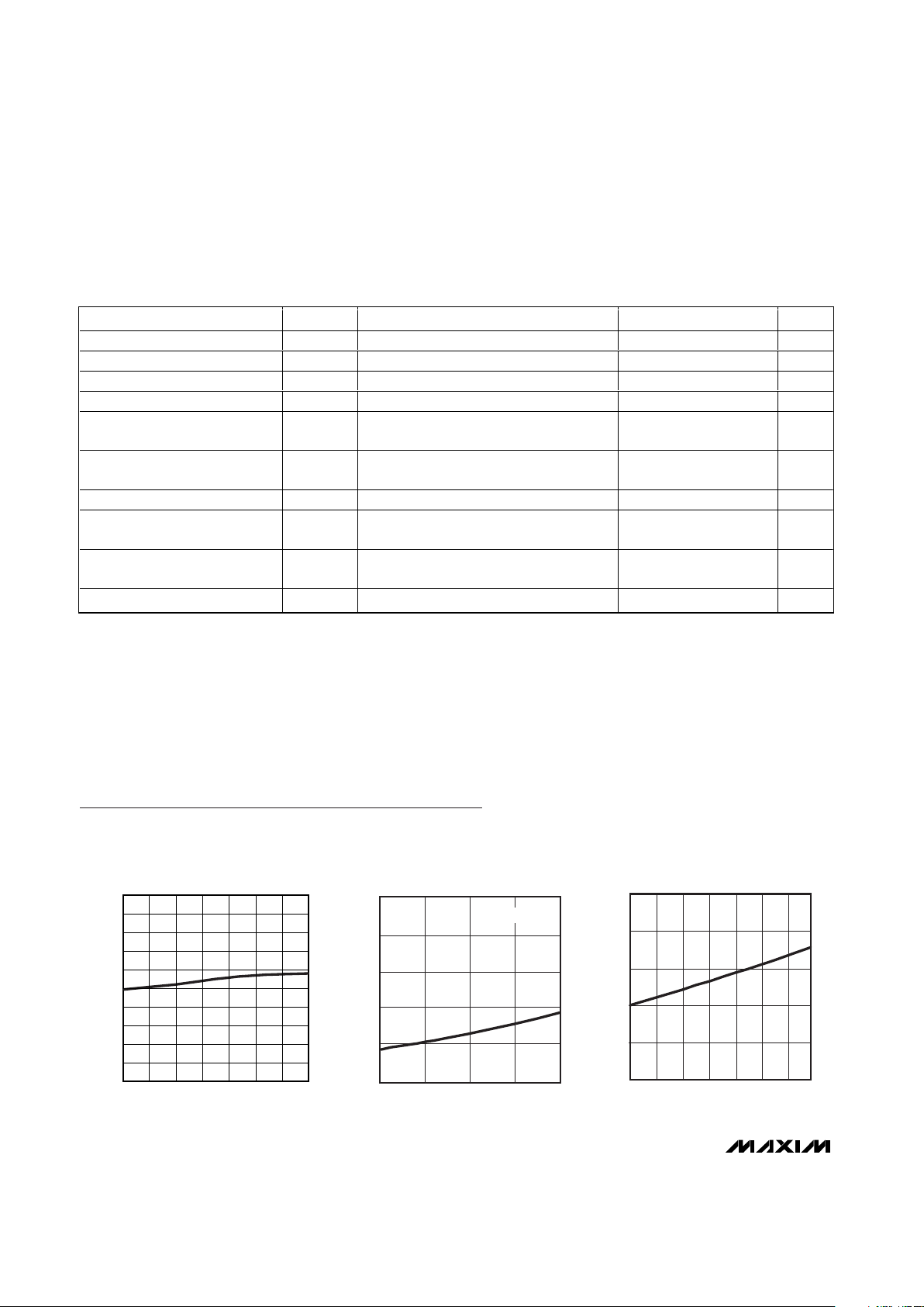
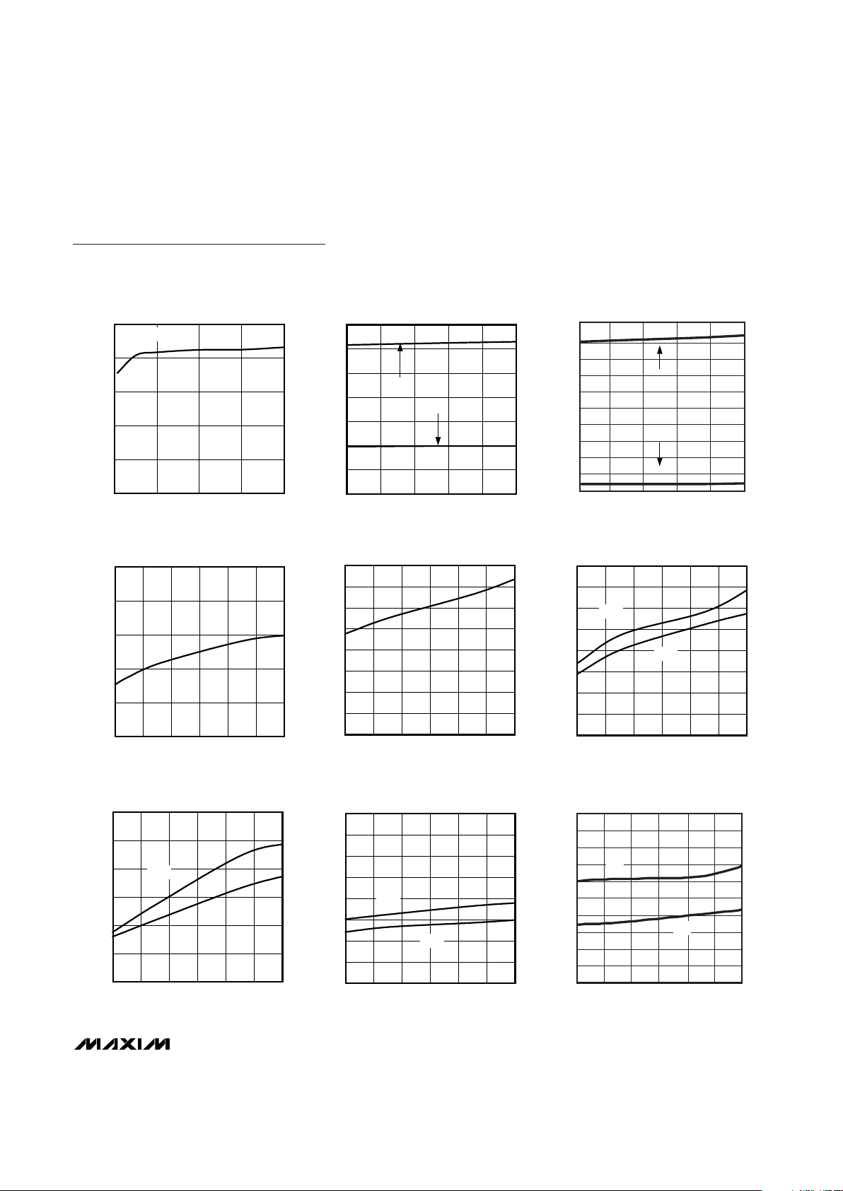
Typical Operating Characteristics
(VCC= 3.3V, VL= 1.8V, C
IOVCC_
= 10pF, C
IOVL_
= 15pF, R
SOURCE
= 150Ω, data rate = 100Mbps, push-pull driver, TA= +25°C,
unless otherwise noted.)
350
360
380
370
390
400
2.2 2.62.4 2.8 3.0 3.2
VL SUPPLY CURRENT vs. VCC SUPPLY
VOLTAGE (DRIVING ONE I/O V
L_
)
MAX13042E toc01
VCC SUPPLY VOLTAGE (V)
V
L
SUPPLY CURRENT (µA)
340
330
320
310
300
3.4 3.6
0
2
6
4
8
10
1.6 2.42.0 2.8 3.2
VL SUPPLY CURRENT vs. VL SUPPLY
VOLTAGE (DRIVING ONE I/O V
CC_
)
MAX13042E toc02
VL SUPPLY VOLTAGE (V)
V
L
SUPPLY CURRENT (mA)
VCC = 3.6V
0
3
9
6
12
15
2.2 2.8 3.0 3.2
VCC SUPPLY CURRENT vs. VCC SUPPLY
VOLTAGE (DRIVING ONE I/O V
L_
)
MAX13042E toc03
VL SUPPLY VOLTAGE (V)
V
CC
SUPPLY CURRENT (mA)
2.4
2.6 3.4
3.6
MAX13042E–MAX13045E
1.62V to 3.6V Improved High-Speed LLT
_______________________________________________________________________________________ 5
Typical Operating Characteristics (continued)
(VCC= 3.3V, VL= 1.8V, C
IOVCC_
= 10pF, C
IOVL_
= 15pF, R
SOURCE
= 150Ω, data rate = 100Mbps, push-pull driver, TA= +25°C,
unless otherwise noted.)
VCC SUPPLY CURRENT vs. VL SUPPLY VOLTAGE
(DRIVING ONE I/O V
CC
_)
VL SUPPLY VOLTAGE (V)
V
CC
SUPPLY CURRENT (mA)
MAX13042E toc04
1.6 2.0 2.4 2.8 3.2
0
2
4
6
8
10
VCC = 3.6V
SUPPLY CURRENT vs. TEMPERATURE
(DRIVING ONE I/O V
CC_
)
TEMPERATURE (°C)
SUPPLY CURRENT (mA)
MAX13042E toc05
-40 -15 10 35 60 85
0
1
2
3
4
5
6
7
I
VCC
I
VL
0
2
6
4
8
10
-40 35
SUPPLY CURRENT vs. TEMPERATURE
(DRIVING ONE I/O V
L_
)
MAX13042E toc06
TEMPERATURE (°C)
SUPPLY CURRENT (mA)
I
VCC
-15
60
85
I
VL
9
1
3
5
7
10
CAPACITIVE LOAD (pF)
V
L
SUPPLY CURRENT (µA)
MAX13042E toc07
10 15 20 25 30 35 40
0
1000
2000
3000
4000
5000
VL SUPPLY CURRENT vs. CAPACITIVE
LOAD ON I/O V
L_
(DRIVING ONE I/O V
CC_
)
V
CC
SUPPLY CURRENT vs. CAPACITIVE
LOAD ON I/O V
CC_
(DRIVING ONE I/O VL_)
CAPACITIVE LOAD (pF)
V
CC
SUPPLY CURRENT (mA)
MAX13042E toc08
10 15 20 25 30 35 40
0
2
4
6
8
10
12
14
16
CAPACITIVE LOAD (pF)
RISE/FALL TIME (ns)
MAX13042E toc09
10 15 20 25 30 35 40
0
0.2
0.4
0.6
0.8
1.0
1.2
1.4
1.6
RISE/FALL TIME vs. CAPACITIVE LOAD ON
I/O V
CC_
(DRIVING I/O VL_)
t
RVCC
t
FVCC
CAPACITIVE LOAD (pF)
RISE/FALL TIME (ns)
MAX13042E toc10
10 15 20 25 30 35 40
0
0.5
1.0
1.5
2.0
2.5
3.0
RISE/FALL TIME vs. CAPACITIVE LOAD ON
I/O V
L_
(DRIVING I/O V
CC_
)
t
FVL
t
RVL
PROPAGATION DELAY vs. CAPACITIVE
LOAD ON I/O V
CC_
(DRIVING I/O VL_)
CAPACITIVE LOAD (pF)
PROPAGATION DELAY (ns)
MAX13042E toc11
10 15 20 25 30 35 40
1.0
1.5
2.0
2.5
3.0
3.5
4.0
4.5
5.0
t
PHL
t
PLH
2.0
3.5
3.0
4.5
5.0
10 25 30
PROPAGATION DELAY vs. CAPACITIVE
LOAD ON I/O V
L_
(DRIVING I/O V
CC_
)
MAX13042E toc12
CAPACITIVE LOAD (pF)
PROPAGATION DELAY (ns)
15
20 35
40
4.0
2.5
1.5
1.0
0.5
0
t
PHL
t
PLH

MAX13042E–MAX13045E
1.62V to 3.6V Improved High-Speed LLT
6 _______________________________________________________________________________________
Pin Description
PIN
UCSP TDFN
NAME FUNCTION
A1 8
I/O VCC4
Input/Output 4. Referenced to VCC.
A2 10
I/O VCC3
Input/Output 3. Referenced to VCC.
A3 12
I/O VCC2
Input/Output 2. Referenced to VCC.
A4 14
I/O VCC1
Input/Output 1. Referenced to VCC.
B1 9 V
CC
Power-Supply Voltage, +2.2V to +3.6V. Bypass VCC to GND with a
0.1µF ceramic capacitor. For full ESD protection, connect an
additional 1µF ceramic capacitor from V
CC
to GND as close to the
V
CC
input as possible.
B2 6 V
L
Logic Supply Voltage, +1.62V to +3.2V. Bypass VL to GND with a
0.1µF ceramic capacitor placed as close to the device as possible.
B3 2 EN
Enable Input. Drive EN to GND for shutdown mode, or drive EN to
V
L
or VCC for normal operation.
B4 13 GND Ground
C1 7
I/O VL4
Input/Output 4. Referenced to VL.
C2 5
I/O VL3
Input/Output 3. Referenced to VL.
C3 3
I/O VL2
Input/Output 2. Referenced to VL.
C4 1
I/O VL1
Input/Output 1. Referenced to VL.
— 4, 11 N.C. No Connection. Leave N.C. unconnected.
— EP EP Exposed Pad. Connect exposed pad to GND.
Typical Operating Characteristics (continued)
(VCC= 3.3V, VL= 1.8V, C
IOVCC_
= 10pF, C
IOVL_
= 15pF, R
SOURCE
= 150Ω, data rate = 100Mbps, push-pull driver, TA= +25°C,
unless otherwise noted.)
TYPICAL I/O VL_ DRIVING
(FREQUENCY = 26MHz, C
IOVCC_
= 40pF)
MAX1342E toc13
I/O V
L_
1V/div
I/O V
CC_
2V/div
10ns/div
TYPICAL I/O V
CC_
DRIVING
(FREQUENCY = 26MHz, C
IOVL_
= 15pF)
MAX1342E toc14
I/O V
L_
1V/div
I/O V
CC_
2V/div
10ns/div
MAX13042E–MAX13045E
1.62V to 3.6V Improved High-Speed LLT
_______________________________________________________________________________________ 7
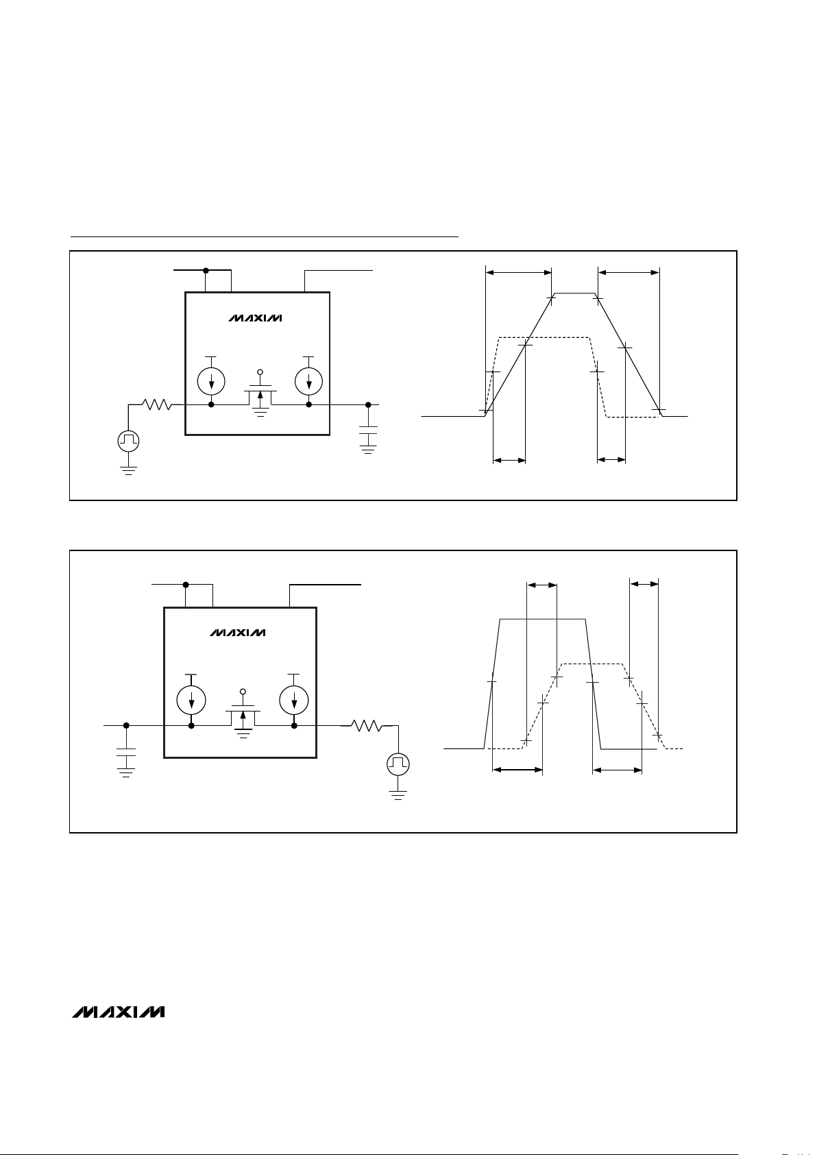
Test Circuits/Timing Diagrams
MAX13042E–MAX13045E
t
FVCC
t
RVCC
I/O V
L_
I/O V
CC_
150Ω
V
L
V
L
V
CC
10%
10%
90%
90%
50%
50%
50%
50%
V
CC
C
IOVCC
t
PLH
t
PHL
t
PVL-VCC
= t
PLH
OR t
PHL
V
CC
EN
V
L
I/O V
CC_
I/O V
L_
Figure 1. Push-Pull Driving I/O VL_Test Circuit and Timing
MAX13042E–MAX13045E
t
FVL
t
RVL
V
L
V
L
V
CC
10%
10%
90%
90%
50%
50%
50%
50%
V
CC
C
IOVL
I/O V
CC_
V
L
V
CC
EN
150Ω
I/O V
L_
I/O V
L_
I/O V
CC_
t
PLH
t
PHL
t
PVCC-VL
= t
PLH
OR t
PHL
Figure 2. Push-Pull Driving I/O V
CC_
Test Circuit and Timing

MAX13042E–MAX13045E
1.62V to 3.6V Improved High-Speed LLT
8 _______________________________________________________________________________________
MAX13042E–
MAX13045E
SOURCE
I/O V
CC_
C
IOVCC
R
LOAD
EN
V
L
0V
V
L
V
CC
0V
0V
I/O V
L_
I/O V
CC_
V
CC
/ 2
EN
V
L
I/O V
L_
SOURCE
C
IOVCC
I/O V
CC_
EN
I/O V
L_
R
LOAD
V
CC
t'
EN-VCC
EN
V
L
0V
V
L
V
CC
0V
0V
I/O V
L_
t
EN-VCC
IS WHICHEVER IS LARGER BETWEEN t'
EN-VCC
AND t"
EN-VCC
.
I/O V
CC_
V
CC
/ 2
t"
EN-VCC
V
L
V
CC
V
L
V
CC
V
L
V
CC
V
L
V
CC
MAX13042E–
MAX13045E
SOURCE
V
CC
EN
V
L
0V
V
CC
V
L
0V
0V
I/O V
CC_
I/O V
L_
VL / 2
EN
I/O V
L_
I/O V
CC_
SOURCE
EN
t'
EN-VL
EN
V
L
0V
V
CC
V
L
0V
0V
I/O V
CC_
t
EN-VCC
IS WHICHEVER IS LARGER BETWEEN t'
EN-VCC
AND t"
EN-VCC
.
I/O V
L_
VL / 2
t"
EN-VL
C
IOVL
R
LOAD
R
LOAD
C
IOVL
I/O V
L_
I/O V
CC_
V
L
MAX13042E–
MAX13045E
MAX13042E–
MAX13045E
Figure 3. Enable Test Circuit and Timing
Test Circuits/Timing Diagrams (continued)

MAX13042E–MAX13045E
1.62V to 3.6V Improved High-Speed LLT
_______________________________________________________________________________________ 9
Detailed Description
The MAX13042E–MAX13045E 4-channel, bidirectional
level translators provide the level shifting necessary for
100Mbps data transfer in multivoltage systems. The
MAX13042E–MAX13045E are ideally suited for level
translation in systems with four channels. Externally
applied voltages, VCCand VL, set the logic levels on
either side of the device. Logic signals present on the
VLside of the device appear as a high-voltage logic
signal on the VCCside of the device and vice-versa.
The MAX13042E–MAX13045E operate at full speed
with external drivers that source as little as 4mA output
current. Each I/O channel is pulled up to VCCor VLby
an internal 30µA current source, allowing the
MAX13042E–MAX13045E to be driven by either pushpull or open-drain drivers.
The MAX13042E–MAX13045E feature an enable (EN)
input that places the devices into a low-power shutdown
mode when driven low. The MAX13042E–MAX13045E
feature an automatic shutdown mode that disables the
part when VCCis less than VL. The state of I/O V
CC_
and
I/O VL_during shutdown is chosen by selecting the
appropriate part version (see the Ordering Information/
Selector Guide).
The MAX13042E–MAX13045E operate with VCCvoltages from +2.2V to +3.6V and VLvoltages from +1.62V
to +3.2V.
Level Translation
For proper operation, ensure that +2.2V ≤ V
CC
≤ +3.6V, +1.62V ≤ VL≤ VCC- 0.2V. When power is
supplied to VL while VCCis missing or less than VL, the
MAX13042E–MAX13045E automatically enter a lowpower mode. The devices will also enter shutdown mode
when EN = 0V. This allows VCCto be disconnected and
still have a known state on I/O VL_. The maximum data
rate depends heavily on the load capacitance (see the
Rise/Fall Time vs. Capacitive Load graphs in the Typical
Operating Characteristics), output impedance of the
driver, and the operating voltage range.
Input Driver Requirements
The MAX13042E–MAX13045E architecture is based on
an nMOS pass gate and output accelerator stages
(Figure 6). The accelerators are active only when there
is a rising/falling edge on a given I/O. A short pulse is
then generated where the output accelerator stages
become active and charge/discharge the capacitances
at the I/Os. Due to its architecture, both input stages
become active during the one-shot pulse. This can lead
to current feeding into the external source that is driving
the translator. However, this behavior helps to speed
up the transition on the driven side.
The MAX13042E–MAX13045E have internal current
sources capable of sourcing 30µA to pull up the I/O
lines. These internal-pullup current sources allow the
inputs to be driven with open-drain drivers as well as
push-pull drivers. It is not recommended to use external
pullup resistors on the I/O lines. The architecture of the
MAX13042E–MAX13045E permits either side to be driven with a minimum of 4mA drivers or larger.
Output Load Requirements
The MAX13042E–MAX13045E I/O are designed to drive
CMOS inputs. Do not load the I/O lines with a resistive
load less than 25kΩ and do not place an RC circuit at
the input of these devices to slow down the edges. If a
slower rise/fall time is required, refer to the MAX3000E/
MAX3001E logic-level translator data sheet.
MAX13042E–MAX13045E
V
L
V
CC
I/O VL1
I/O V
L
2
I/O V
L
3
I/O V
L
4
I/O V
L
1
I/O V
CC
1
I/O V
CC
2
I/O VCC3
I/O V
CC
4
GND
EN
Functional Diagram

MAX13042E–MAX13045E
1.62V to 3.6V Improved High-Speed LLT
10 ______________________________________________________________________________________
Shutdown Mode
The MAX13042E–MAX13045E feature an enable (EN)
input that places the devices into a low-power shutdown
mode when driven low. The MAX13042E–MAX13045E
feature an automatic shutdown mode that disables the
part when VCCis unconnected or less than VL.
Applications Information
Layout Recommendations
Use standard high-speed layout practices when
laying out a board with the MAX13042E–MAX13045E.
For example, to minimize line coupling, place all other
signal lines not connected to the MAX13042E–
MAX13045E at least 1x the substrate height of the
PCB away from the input and output lines of the
MAX13042E–MAX13045E.
Power-Supply Decoupling
To reduce ripple and the chance of introducing data
errors, bypass VLand VCCto ground with 0.1µF ceramic capacitors. Place all capacitors as close to the
power-supply inputs as possible. For full ESD protection, bypass VCCwith a 1µF ceramic capacitor located
as close to the VCCinput as possible.
Unidirectional vs. Bidirectional
Level Translator
The MAX13042E–MAX13045E bidirectional level translators can operate as a unidirectional device to trans-
late signals without inversion. These devices provide
the smallest solution (UCSP package) for unidirectional
level translation without inversion.
ESD Test Conditions
ESD performance depends on a variety of conditions.
Contact Maxim for a reliability report that documents
test setup, test methodology, and test results.
Use with External Pullup/
Pulldown Resistors
Due to the architecture of the MAX13042E–MAX13045E,
it is not recommended to use external pullup or pulldown resistors on the bus. In certain applications, the
use of external pullup or pulldown resistors is desired to
have a known bus state when there is no active driver
on the bus. The MAX13042E–MAX13045E include internal pullup current sources that set the bus state when
the device is enabled. In shutdown mode, the state of
I/O V
CC_
and I/O VL_is dependent on the selected part
version (see the Ordering Information/Selector Guide).
Open-Drain Signaling
The MAX13042E–MAX13045E are designed to pass opendrain as well as CMOS push-pull signals. When used with
open-drain signaling, the rise time will be dominated by the
interaction of the internal pullup current source and the parasitic load capacitance. The MAX13042E–MAX13045E
include internal rise-time accelerators to speed up transitions, eliminating any need for external pullup resistors. For
applications such as I2C or 1-wire that require an external
pullup resistor, please consult the MAX3378E and
MAX3396E data sheets.
UCSP Applications Information
For the latest application details on UCSP construction,
dimensions, tape carrier information, PCB techniques,
bump-pad layout, and recommended reflow temperature
profiles, as well as the latest information on reliability testing
results, go to Maxim’s website at www.maxim-ic.com/ucsp
to find the Application Note: UCSP – A Wafer-Level Chip-
Scale Package.
Chip Information
PROCESS: BiCMOS
30µA
V
L
ENABLE
ENABLE
ENABLE
V
CC
30µA
BOOST
CIRCUIT
I/O V
L_
V
L
V
CC
BOOST
CIRCUIT
V
CC
V
L
I/O V
CC_
NOTE: THE MAX13042E–MAX13045E ARE ENABLED WHEN
V
L
<
VCC AND EN = VL.
Figure 4. Simplified Functional Diagram for One I/O Line

MAX13042E–MAX13045E
1.62V to 3.6V Improved High-Speed LLT
______________________________________________________________________________________ 11
TDFN
(3mm x 3mm)
I/O V
L
1
4
3
2
1
11
12
13
14
N.C.
I/O V
L
2
EN
7
6
5
I/O VL4
V
L
I/O VL3
N.C.
I/O V
CC
2
GND
I/O V
CC
1
8
9
10
I/O VCC4
V
CC
I/O VCC3
MAX13042E–MAX13045E
*EP
+
*CONNECT EXPOSED PAD TO GROUND
UCSP
(1.54mm x 2.12mm)
A
B
C
12 3
4
I/O VCC3
I/O V
CC
1
I/O V
CC
4
I/O VCC2
V
L
GND
V
CC
EN
MAX13042E–MAX13045E
I/O V
L
3
I/O V
L
1
I/O V
L
4
I/O V
L
2
TOP VIEW
(BUMPS ON BOTTOM)
TOP VIEW
+
Pin Configurations
Ordering Information/Selector Guide (continued)
PART
PINPACKAGE
I/O VL_ STATE DURING
SHUTDOWN
I/O V
CC_
STATE DURING
SHUTDOWN
TOP
MARK
PKG CODE
MAX13043EEBC+T
12 UCSP-12 High Impedance 16.5kΩ to GND ADR B12-3
MAX13043EETD+T
14 TDFN-EP**
High Impedance 16.5kΩ to GND ADF T1433-2
MAX13044EEBC+T*
12 UCSP-12 16.5kΩ to GND High Impedance ADS B12-3
MAX13044EETD+T*
14 TDFN-EP**
16.5kΩto GND High Impedance
ADG
T1433-2
MAX13045EEBC+T*
12 UCSP-12 16.5kΩ to GND 16.5kΩ to GND ADT B12-3
MAX13045EETD+T*
14 TDFN-EP**
16.5kΩ to GND 16.5kΩ to GND ADH T1433-2
Note: All devices operate over the -40°C to +85°C temperature
range.
+Denotes a lead-free package.
*Future product—contact factory for availability.
**EP = Exposed paddle.

MAX13042E–MAX13045E
1.62V to 3.6V Improved High-Speed LLT
12 ______________________________________________________________________________________
Package Information
(The package drawing(s) in this data sheet may not reflect the most current specifications. For the latest package outline information,
go to www.maxim-ic.com/packages
.)
12L, UCSP 4x3.EPS
F
1
1
21-0104
PACKAGE OUTLINE, 4x3 UCSP

MAX13042E–MAX13045E
1.62V to 3.6V Improved High-Speed LLT
______________________________________________________________________________________ 13
Package Information (continued)
(The package drawing(s) in this data sheet may not reflect the most current specifications. For the latest package outline information,
go to www.maxim-ic.com/packages
.)
6, 8, &10L, DFN THIN.EPS

MAX13042E–MAX13045E
1.62V to 3.6V Improved High-Speed LLT
Maxim cannot assume responsibility for use of any circuitry other than circuitry entirely embodied in a Maxim product. No circuit patent licenses are
implied. Maxim reserves the right to change the circuitry and specifications without notice at any time.
14 ____________________Maxim Integrated Products, 120 San Gabriel Drive, Sunnyvale, CA 94086 408-737-7600
© 2007 Maxim Integrated Products is a registered trademark of Maxim Integrated Products, Inc.
Springer
Package Information (continued)
(The package drawing(s) in this data sheet may not reflect the most current specifications. For the latest package outline information,
go to www.maxim-ic.com/packages
.)
COMMON DIMENSIONS
SYMBOL MIN. MAX.
A 0.70 0.80
D 2.90 3.10
E 2.90 3.10
A1
0.00 0.05
L 0.20 0.40
PKG. CODE N D2 E2 e JEDEC SPEC b
[(N/2)-1] x e
PACKAGE VARIATIONS
0.25 MIN.k
A2 0.20 REF.
2.00 REF0.25–0.050.50 BSC2.30–0.1010T1033-1
2.40 REF0.20–0.05- - - - 0.40 BSC1.70–0.10 2.30–0.1014T1433-1
1.50–0.10 MO229 / WEED-3
0.40 BSC - - - - 0.20–0.05 2.40 REFT1433-2 14 2.30–0.101.70–0.10
T633-2 6 1.50–0.10 2.30–0.10 0.95 BSC MO229 / WEEA 0.40–0.05 1.90 REF
T833-2 8 1.50–0.10 2.30–0.10 0.65 BSC MO229 / WEEC 0.30–0.05 1.95 REF
T833-3 8 1.50–0.10 2.30–0.10 0.65 BSC MO229 / WEEC 0.30–0.05 1.95 REF
2.30–0.10 MO229 / WEED-3 2.00 REF0.25–0.050.50 BSC1.50–0.1010T1033-2
 Loading...