

General Description
The MAX13036 automotive contact monitor and level
shifter monitors and debounces eight remote mechanical
switches and asserts an interrupt (INT) if a switch
changes state. The state of each switch is sampled
through an SPI™ interface by reading the status register
and any switch can be prohibited from asserting an interrupt by writing to the command register. Four of the
switch inputs are intended for ground-connected switches (IN0–IN3), and the other four inputs (IN4–IN7), are
programmable in groups of two for either ground-connected or battery-connected switches. Two switch inputs
(IN0, IN1) have direct level-shifted outputs (DO0, DO1)
to be used for PWM or other timing-based signals.
Switch input thresholds are set to 50% of the voltage
applied to BATREF. The threshold hysteresis is set by
connecting an external resistor from HYST to ground.
The MAX13036 supplies an adjustable wetting current to
each closed switch to clean mechanical switch contacts
that are exposed to adverse conditions.
The MAX13036 operates with a +6V to +26V battery voltage applied to BAT. A separate +2.7V to +5.5V logic supply input (V
L
) sets the interface voltage. The MAX13036 is
available in a 5mm x 5mm 28-pin TQFN package and
operates over the -40°C to +125°C temperature range.
Applications
Features
o +6V to +26V Operating Voltage Range
o +42V Compatibility on BAT
o Inputs Withstand Reverse Battery
o Withstands Dynamic Battery Voltage Drop While
V
L
is Present
o Ultra-Low Operating Current 17µA (typ) in
Scan Mode
o Resistor-Adjustable Switching Hysteresis
o CMOS-Compatible Logic Outputs (+2.7V min)
o Built-In Switch Debouncing
o Interrupt Output
o Immunity to Transients
o High Modularity
o Thermal Protection
o ±8kV HBM ESD Protection on IN0–IN7 Without
External Components
o Two Inputs (IN0, IN1) Programmable as Direct
Outputs
o Four Inputs (IN4–IN7) Programmable for BAT or
GND Related Switches
MAX13036
Automotive Contact Monitor
and Level Shifter
________________________________________________________________
Maxim Integrated Products
1
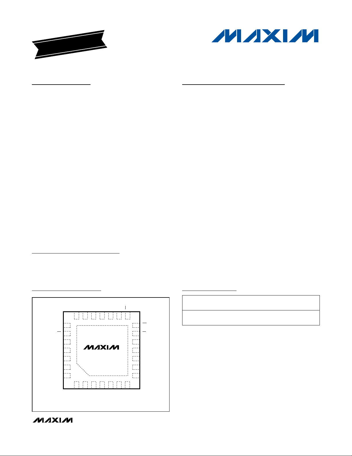
Pin Configuration
19-0808; Rev 0; 4/07
For pricing, delivery, and ordering information, please contact Maxim/Dallas Direct! at
1-888-629-4642, or visit Maxim’s website at www.maxim-ic.com.
EVALUATION KIT
AVAILABLE
Ordering Information
+
Denotes lead-free package.
*
EP = Exposed paddle.
Body Computers
Window Lifters
Seat Movers
Electric Sunroofs
Other Control ECUs
Typical Application Circuit appears at end of data sheet.
SPI is a trademark of Motorola, Inc.
TOP VIEW
DO0
SD
GND
BATREF
BAT
N.C.
INO
*CONNECT EXPOSED PADDLE TO GROUND
DO1
21
22
*EP
23
24
25
26
27
+
28
1
IN1
N.C.
20
2
IN2
L
CLK
V
19
18
MAX13036
3
4
IN3
IN4
TQFN
SDI
SDO
CS
17
16
15
INT
14
13
OT
12
GND
11
TDEB
10
WET
9
HYST
N.C.
8
5
6
7
IN6
IN5
IN7
PART TEMP RANGE
MAX13036ATI+ -40°C to +125°C
PINPACKAGE
28 TQFN-EP*
(5mm x 5mm)
PKG
CODE
T2855-8
MAX13036
Automotive Contact Monitor
and Level Shifter
2 _______________________________________________________________________________________
ABSOLUTE MAXIMUM RATINGS
ELECTRICAL CHARACTERISTICS
(VL= +2.7V to +5.5V, BAT = +6V to +26V, SD = VL, TA= -40°C to +125°C, unless otherwise noted. Typical values are at VL= +3.3V,
BAT = +14V, T
A
= +25°C) (Note 1)
Stresses beyond those listed under “Absolute Maximum Ratings” may cause permanent damage to the device. These are stress ratings only, and functional
operation of the device at these or any other conditions beyond those indicated in the operational sections of the specifications is not implied. Exposure to
absolute maximum rating conditions for extended periods may affect device reliability.
(All voltages referenced to GND, unless otherwise noted.)
V
L
...........................................................................-0.3V to +6.0V
BAT.........................................................................-0.3V to +42V
BATREF, IN_ to BAT ................................................-45V to +45V
BATREF, IN_ to GND...............................................-45V to +45V
SD...........................................................................-0.3V to +45V
HYST, WET, TDEB, OT, INT .....................................-0.3V to 6.0V
CS, CLK, SDI, SDO, DO0, DO1 ....................-0.3V to (V
L
+ 0.3V)
Continuous Current (CS, CLK, SDI, SDO, DO0, DO1) .....±20mA
HBM ESD Protection (IN0–IN7)............................................±8kV
Continuous Power Dissipation (T
A
= +70°C, multilayer board)
28-Pin TQFN (derate 34.5mW/°C above +70°C) .......2759mW
Operating Temperature Range .........................-40°C to +125°C
Junction Temperature......................................................+150°C
Storage Temperature Range .............................-65°C to +150°C
Lead Temperature (soldering, 10s) .................................+300°C
POWER SUPPLY
VL Supply Range V
VL Supply Current I
BAT Supply Range V
Total Supply Current I
Total Supply Current in Scan
Mode
PARAMETER SYMBOL CONDITIONS MIN TYP MAX UNITS
L
VL = +5.5V, V
L
BAT
VL = +5V, V
scan, programmable hysteresis off,
SUP
M0 = M1 =1, WEND = 1, IN0–IN7 =
unconnected,
CS = V
L
V
= +14V, scan mode (SC0 = 0,
I
SUP_SCAN
BAT
SC1= 0, SC2 = 0), CS = V
SDI = CLK = GND (Note 2)
2.7 5.5 V
= +14V 0 1 µA
BAT
626V
= +14V, continuous
BAT
46 80 µA
, SDI = CLK = GND (Note 2)
,
L
17 36 µA
Total Supply Current in Shutdown
Mode
BATREF Input Leakage Current in
Shutdown
BATREF Input Resistance R
VSD = 0V,
V
I
SHDN
BAT
V
B AT RE F
(Note 2)
I
L_BATREFVSD
BATREFVBATREF
= +14V,
= + 14V
= 0V, V
= +14V 1 MΩ
TA = +25°C 2 3.2
T
= -40°C to +125°C 2 4.0
A
= +14V 1 µA
BATREF
SWITCH INPUTS (IN0–IN7)
R
Input-Voltage Threshold Center
(Note 3)
Input-Voltage Threshold
Hysteresis (Note 4)
V
TH_C
V
TH_HYS
= ∞ or programmable hysteresis
HYST
disabled
R
= 90kΩ
HYST
R
= ∞ or programmable hysteresis
HYST
disabled
R
= 90kΩ
HYST
R
= 0Ω
HYST
0.425 x
V
BATREF
0.4 x
V
BATREF
0.133 x
V
BATREF
0.26 x
V
BATREF
0.5 x
V
BATREF
0.5 x
V
BATREF
0.166 x
V
BATREF
0.361 x
V
BATREF
0.5 x
V
BATREF
0.575 x
V
BATREF
0.63 x
V
BATREF
0.22 x
V
BATREF
0.48 x
V
BATREF
µA
V
V
MAX13036
Automotive Contact Monitor
and Level Shifter
_______________________________________________________________________________________ 3
ELECTRICAL CHARACTERISTICS (continued)
(VL= +2.7V to +5.5V, BAT = +6V to +26V, SD = VL, TA= -40°C to +125°C, unless otherwise noted. Typical values are at VL= +3.3V,
BAT = +14V, T
A
= +25°C) (Note 1)
Switch-State Sense Resistor R
Wetting Current Rise/Fall Time
Wetting Current I
IN0–IN7 Input Impedance in
Shutdown
LOGIC-LEVELS
SDO, DO0, DO1 Output
Voltage High
SDO, DO0, DO1 Output
Voltage Low
INT, OT Output Voltage Low V
SD Input Leakage Current I
SD Input-Voltage Low V
SD Input-Voltage High V
CS, CLK, SDI Input-Voltage Low V
CS, CLK, SDI Input-Voltage High V
CS, CLK Input Leakage Current I
INT, OT Leakage Current I
SDI Input Impedance R
THERMAL SHUTDOWN
Thermal Shutdown Temperature T
Thermal Shutdown Hysteresis T
PARAMETER SYMBOL CONDITIONS MIN TYP MAX UNITS
SENSE
I
WET_RISE_
FALL
WET
V
OH
V
OL
INTL
L_SD
IL_SD
IH_SD
IL
IH
IL
OL
SDI
SHDN
HYST
R
= 61kΩ
WET
(Note 5)
R
= 61kΩ 22
WET
R
= 30kΩ, V
WET
R
= 330kΩ 7.5
WET
= 0V, V
V
SD
Source current = 2mA 0.8 x V
Sink current = 4mA 0.2 x V
Sink current = 4mA 0.4 V
VSD = V
IN
= +12V 15 30 µA
BAT
Rise 6
Fall 1
= 14V 28 40 51
BAT
_ = +14V 5.5 8.5 MΩ
11 16 22 kΩ
L
L
0.8
2.4 V
0.33 x
V
L
0.66 x
V
L
-1 +1 µA
-1 +1 µA
65 100 145 kΩ
+170 °C
15 °C
µs
mA
V
V
V
V
V

MAX13036
Automotive Contact Monitor
and Level Shifter
4 _______________________________________________________________________________________
TIMING CHARACTERISTICS
(VL= +2.7V to +5.5V, BAT = +6V to +26V, SD = VL, TA= -40°C to +125°C, unless otherwise noted. Typical values are at VL= +3.3V,
BAT = +14V, T
A
= +25°C) (Note 1)
)
Note 1: All units are 100% production tested at TA= +125°C. Limits over the operating temperature range are guaranteed by
correlation to the +125°C tests.
Note 2: The total supply current is the sum of the current flowing into V
L
, BAT, and BATREF.
Note 3: V
TH_C
= (V
TH_HIGH
+ V
TH_LOW
)/2.
Note 4: V
TH_HYS
= (V
TH_HIGH
- V
TH_LOW
).
Note 5: Wetting current rise/fall time is measured as the time from 10% to 90% of the maximum wetting current.
Note 6: Guaranteed by design.
IN0 to DO0 Propagation Delay V
IN1 to DO1 Propagation Delay
CLK Frequency f
Falling Edge of CS to Rising Edge
of CLK Required Setup Time
Falling Edge of CLK to Rising
Edge of CS Required Setup Time
SDI Valid to Falling Edge of CLK
Required Setup Time
Falling Edge of CLK to SDI
Required Hold Time
Time From Falling Edge of CS to
SDO Low Impedance
Time From Rising Edge of CS to
SDO High Impedance
Time from Rising Edge of CLK to
SDO Data Valid
Debounce time t
Scanning Time Pulse t
Scanning Time Period t
Wetting Time Pulse t
Time from Shutdown To Normal
Operation
PARAMETER SYMBOL CONDITIONS MIN TYP MAX UNITS
= 6V 22 35
t
PROP
CLK
t
LEAD
t
LAG
t
SI(SU)
t
SI(HOLD
t
SO(EN)
t
SO(DIS)VL
t
VALID
DEB
SCAN
SCAN_P
WET
BAT
V
= +14V 22
BAT
Input rise/fall time < 2ns,
V
= +3.0V to +5.5V
L
Input rise/fall time < 2ns,
V
= +3.0V to +5.5V, Figure 1
L
Input rise/fall time < 2ns,
V
= +3.0V to +5.5V, Figure 1
L
Input rise/fall time < 2ns,
V
= +3.0V to +5.5V, Figure 1
L
Input rise/fall time < 2ns,
V
= +3.0V to +5.5V, Figure 1
L
Input rise/fall time < 2ns,
V
= +3.0V to +5.5V, Figure 1
L
110 ns
50 ns
30 ns
20 ns
5 MHz
55 ns
= +3.0V to +5.5V, Figures 1 and 2 55 ns
C
=15pF,
SDO
= +3.0V to +5.5V, Figure 1
V
L
C
= 500pF 3.18 5.9 9.42
TDEB
C
= 10nF (Note 6) 63 120 188
TDEB
70 ns
130 250 400 µs
SC2 = 0, SC1 = 1, SC0 = 1 4 8 14 ms
WTOFF = 0 10 21 35 ms
SD low-to-high transition to input
monitoring enabled
200 µs
µs
ms
MAX13036
Automotive Contact Monitor
and Level Shifter
_______________________________________________________________________________________ 5
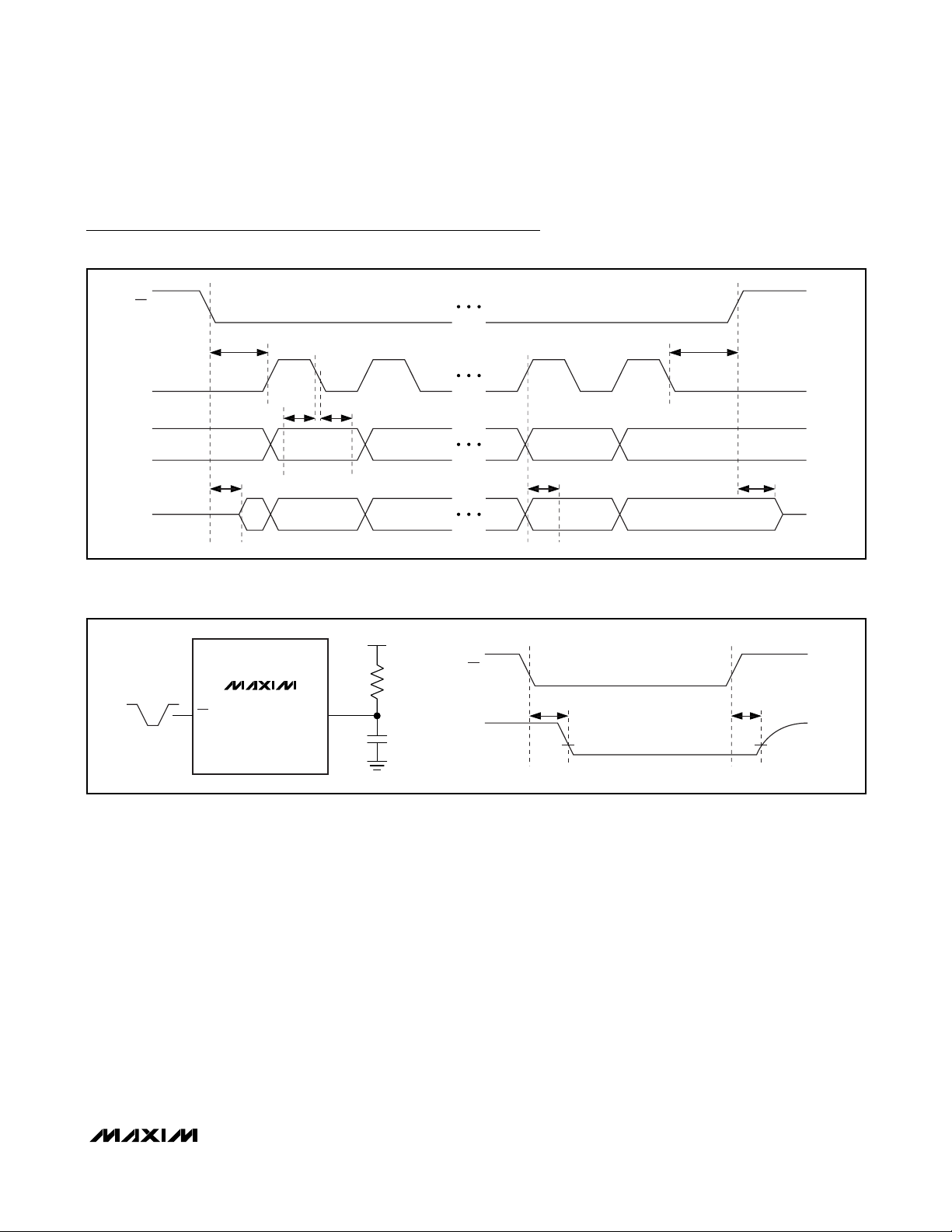
Test Circuits/Timing Diagrams
Figure 1. SPI Timing Characteristics
Figure 2. SDO Enable/Disable Test Circuit and Timing Diagram
CS
t
LEAD
CLK
SDI MSB IN
t
SO(EN)
SDO
MAX13036
t
SI(SU)tSI(HOLD)
t
VALID
MSB OUT LSB OUT
V
L
SDO
CS
t
SO(EN)
1/3V
L
1kΩ
SDOCS
15pF
t
LAG
t
SO(DIS)
t
SO(DIS)
VOL + 0.1V
L
MAX13036
Automotive Contact Monitor
and Level Shifter
6 _______________________________________________________________________________________
Typical Operating Characteristics
(VL= +3.3V, BAT = +14V, SD = VL, R
WET
= 61kΩ, R
HYST
= 90kΩ, C
TDEB
= 4700pF, TA= +25°C, unless otherwise noted.)
WETTING CURRENT vs. V
BAT
V
BAT
(V)
WETTING CURRENT (mA)
MAX13036 toc01
6 1014182226
-30
-20
-10
0
10
20
30
40
GND-CONNECTED SWITCH
BAT-CONNECTED SWITCH
WETTING CURRENT vs. R
WET
R
WET
(kΩ)
WETTING CURRENT (mA)
MAX13036 toc02
30 80 130 180 230 280 330
-60
-50
-40
-30
-20
-10
0
10
20
30
40
50
60
GND-CONNECTED SWITCH
BAT-CONNECTED SWITCH
WETTING CURRENT PULSE
(NORMAL MODE, WTOFF = 0, WEN = WEND = 1)
MAX13036 toc03
20ms/div
V
IN_
10V/div
I
IN_
20mA/div
INT
2V/div
BAT CURRENT vs. TEMPERATURE
(NORMAL MODE)
TEMPERATURE (°C)
I
BAT
(μA)
MAX13036 toc04
-40 -25 -10 5 20 35 50 65 80 95 110 125
0
10
20
30
40
50
60
70
80
90
100
ADJUSTABLE HYSTERESIS OFF
ADJUSTABLE HYSTERESIS ON
BAT CURRENT vs. TEMPERATURE
(SHUTDOWN MODE)
TEMPERATURE (°C)
I
BAT
(μA)
MAX13036 toc05
-40 -25 -10 5 20 35 50 65 80 95 110 125
0
1
2
3
4
5
SD = LOW
BAT CURRENT vs. TEMPERATURE
(SCAN MODE)
TEMPERATURE (°C)
I
BAT
(μA)
MAX13036 toc06
-40 -25 -10 5 20 35 50 65 80 95 110 125
0
5
10
15
20
25
30
SCANNING PERIOD = 64ms
SCANNING PERIOD = 2ms
TYPICAL IN0 DRIVING
(NORMAL MODE, WTOFF = WEN = WEND = 0)
MAX13036 toc07
40μs/div
V
IN0
5V/div
V
DO0
2V/div
f = 5kHz
TYPICAL IN0 DRIVING
(NORMAL MODE, WTOFF = WEN = WEND = 0)
MAX13036 toc08
2ms/div
V
IN0
5V/div
V
DO0
2V/div
f = 100Hz
ADJUSTABLE HYSTERESIS OFF
HYSTERESIS vs. R
HYST
R
(Ω)
HYSTERESIS (V)
MAX13036 toc09
0 200k 400k 600k 800k 1M
0
1
2
3
4
5
6
7
8
ADJUSTABLE HYSTERESIS ON

MAX13036
Automotive Contact Monitor
and Level Shifter
_______________________________________________________________________________________
7
)
Typical Operating Characteristics (continued)
(VL= +3.3V, BAT = +14V, SD = VL, R
WET
= 61kΩ, R
HYST
= 90kΩ, C
TDEB
= 4700pF, TA= +25°C, unless otherwise noted.)
SWITCHING THRESHOLD vs. TEMPERATURE
10
ADJUSTABLE HYSTERESIS OFF
9
8
7
SWITCHING THRESHOLD (V)
6
5
-40 -25 -10 5 20 35 50 65 80 95 110 125
INPUT WAVEFORM IN SCAN MODE
(SCAN MODE, WTOFF = WEN = 0, WEND = 1)
SCANNING PERIOD = 2ms
INPUT SWITCH OPEN
V
IN_
5V/div
VIN_ RISING
VIN_ FALLING
TEMPERATURE (°C)
400μs/div
MAX13036 toc10
MAX13036 toc12
SWITCHING THRESHOLD vs. V
25
ADJUSTABLE HYSTERESIS OFF
20
15
V
RISING
10
SWITCHING THRESHOLD (V)
IN_
5
V
FALLING
IN_
0
6 1014182226
V
(V)
BAT
DEBOUNCE TIME vs. TEMPERATURE
55
54
53
52
51
50
49
48
47
46
45
DEBOUNCE TIME (ms)
44
43
42
41
40
-40-25-10 5 203550658095110125
TEMPERATURE (°C)
BAT
MAX13036 toc11
MAX13036 toc13
DEBOUNCE TIME vs. BAT VOLTAGE
55
54
53
52
51
50
49
48
47
46
45
DEBOUNCE TIME (ms)
44
43
42
41
40
6 1014182226
V
(V
BAT
MAX13036 toc14
120
100
80
60
40
DEBOUNCE TIME (ms)
20
DEBOUNCE TIME vs. C
0
0 2000 4000 6000 8000 10000
C
TDEB
TDEB
(pF)
MAX13036 toc15

MAX13036
Automotive Contact Monitor
and Level Shifter
8 _______________________________________________________________________________________
Pin Description
PIN
FUNCTION
1 IN1
Switch Input Channel 1. Connect IN1 to a switch connected to GND. IN1 can be programmed as a direct
input with a level-shifted output on DO1 (see the Mechanical Switch Inputs (IN0–IN7) section).
2 IN2 Switch Input Channel 2. Connect IN2 to a switch connected to GND.
3 IN3 Switch Input Channel 3. Connect IN3 to a switch connected to GND.
4 IN4 Switch Input Channel 4. Connect IN4 to a switch connected to GND or BAT.
5 IN5 Switch Input Channel 5. Connect IN5 to a switch connected to GND or BAT.
6 IN6 Switch Input Channel 6. Connect IN6 to a switch connected to GND or BAT.
7 IN7 Switch Input Channel 7. Connect IN7 to a switch connected to GND or BAT.
8, 20, 27
N.C. No Connection. Not internally connected.
9 HYST
Hysteresis Input. Connect HYST to GND with a 0 to 900kΩ resistor to set the input voltage hysteresis on
IN0–IN7.
10 WET
Wetting Current Input. Connect a 30kΩ to 330kΩ resistor from WET to GND to set the wetting current on
IN0–IN7.
11 TDEB
Switch Debounce Time Input. Connect a 500pF to 10nF capacitor from TDEB to GND to set the switch
debounce time.
12, 24 GND Ground
13 OT
Overtemperature Warning Output. OT is an open-drain output that asserts low when the thermal warning
threshold is exceeded.
14 INT
Interrupt Output. INT is an open-drain output that asserts low when one or more of the IN0–IN7 inputs
change state and is enabled for interrupts.
15 CS
SPI Chip-Select Input. Drive CS low to enable clocking of data into and out of the MAX13036. SPI data is
latched into the MAX13036 on the rising edge of CS.
16 SDO
SPI Serial Data Output. SPI data is output on SDO on the rising edges of CLK while CS is held low. SDO
is tri-stated when CS is high.
17 SDI
SPI Serial Data Input. SPI data is latched into the internal shift register on the falling edges of CLK while
CS is held low. SDI has an internal 100kΩ pulldown resistor.
18 CLK SPI Serial Clock Input
19 V
L
Logic Power-Supply Input. Connect VL to a positive 2.7V to 5.5V power supply. Bypass VL to ground with
a 0.1µF capacitor placed as close as possible to V
L
.
21 DO1 Data Output Channel 1. DO1 is the level-shifted output of IN1 when WEND = 0 (normal mode only).
22 DO0 Data Output Channel 0. DO0 is the level-shifted output of IN0 when WEND = 0 (normal mode only).
23 SD
Shutdown Input. Drive SD low to place the MAX13036 into shutdown mode. Drive SD high for normal
operation. SD is compatible with voltages up to +45V.
25
Battery Reference Input. Switch thresholds are set to 50% of the voltage applied to BATREF. Connect
BATREF to the system’s battery supply voltage.
26 BAT
Battery Supply Input. Connect BAT to a positive 6V to 26V battery supply voltage. Bypass BAT to ground
with a 0.1µF ceramic capacitor placed as close as possible to BAT. In addition, bypass BAT with a 10µF
or greater capacitor.
28 IN0
Switch Input Channel 0. Connect IN0 to a switch connected to GND. IN0 can be programmed as a direct
input with a level-shifted output on DO0 (see Mechanical Switch Inputs (IN0–IN7) section).
— EP Exposed Paddle. Connect EP to GND.
NAME
BATREF

Detailed Description
The MAX13036 automotive contact monitor and level
shifter monitors and debounces eight remote mechanical
switches and asserts an interrupt (INT) if a switch
changes state. Any of the switch inputs can be prohibited
from asserting an interrupt. The switch threshold levels
are set to 50% of the voltage applied to BATREF. All
switch inputs feature a common adjustable hysteresis,
debounce time and wetting current. Two switch inputs
(IN0, IN1) are programmable to have direct outputs (DO0,
DO1) useable for PWM or other timing based signals.
The MAX13036 features an SPI interface to monitor
individual switch inputs and to configure interrupt
masking, hysteresis and wetting current enable/disable,
switch configuration (battery connected or ground connected), and scanning period.
The MAX13036 features three modes of operation: normal mode, scan mode, and shutdown mode. In normal
mode, the part is fully functional and sensing resistors
are connected to all switch inputs. In scan mode, the
sensing resistors are connected for a finite duration to
reduce power consumption. In shutdown mode, all
switch inputs are high impedance to further reduce
power consumption.
VL
VLis the power-supply input for the digital input/output
buffers. The SPI interface (CS, CLK, SDI, SDO), and
digital outputs (DO0, DO1) are referenced to the voltage on VL. Connect VLto the system’s +2.7V to +5.5V
logic-level supply. Bypass VLto ground with a 0.1µF
capacitor placed as close as possible to the device.
BAT
BAT is the main power-supply input. Bypass BAT to
ground with a 0.1µF ceramic capacitor placed as close
as possible to BAT. In addition, bypass BAT with a
10µF or greater capacitor. BAT can withstand DC voltages up to +42V.
Mechanical Switch Inputs (IN0–IN7)
IN0 through IN7 are the inputs for remote mechanical
switches. The status of each switch input is indicated
by the SW0 through SW7 bits in the status register, and
each switch input can be programmed to not assert an
interrupt (INT) by writing to the P0 through P7 bits in the
command register. All switch inputs are configured to
assert an interrupt upon power-up.
MAX13036
Automotive Contact Monitor
and Level Shifter
_______________________________________________________________________________________ 9
Functional Diagram
MAX13036
LEVEL
TRANSLATORS
WETTING
CURRENT
CONTROL
DIGITAL
INTERFACE
SHIFT
REGISTER
INTERRUPT
LOGIC
SPI
INTERFACE
IN0
BATREF
IN1
IN2
IN3
IN4
IN5
IN6
IN7
HYSTWET TDEB GND
BAT V
L
SD
DO0
DO1
CS
CLK
SDI
SDO
INT
OT

MAX13036
The first four inputs (IN0–IN3) are intended for groundconnected switches. The remaining four inputs (IN4–IN7)
can be programmed in sets of two for either ground-connected or battery-connected switches by writing to the
M0 and M1 bits (see Table 5). The default state after
power-up is IN2–IN7 configured for ground-connected
switches, and IN0/IN1 configured for direct inputs.
All switch inputs have internal 16kΩ sense resistors to
detect switch transitions. Inputs configured for groundconnected switches are pulled up to BAT and inputs
configured for battery-connected switches are pulled
down to GND. Figure 3 shows the switch input structure
for IN0 and IN1. IN0 and IN1 can be programmed as
direct inputs with level-shifted outputs (DO0 and DO1)
by clearing the WEND bit in the command register (normal mode only). When programmed as direct inputs,
IN0 and IN1 can be used for PWM or other signaling.
Clearing the WEND bit disables the sense resistors and
wetting currents on IN0 and IN1. When programmed as
direct inputs, the status of IN0 and IN1 is not reflected
in the status register, and interrupts are not allowed on
these inputs.
Switch Threshold Levels and
Hysteresis (BATREF, HYST)
Input thresholds for the remote switches are 50% of the
voltage applied to BATREF. The BATREF input is typically connected to the battery voltage before the
reverse-battery protection diode. The MAX13036 features adjustable hysteresis on the switch inputs by connecting an external 0 to 900kΩ resistor from HYST to
ground (normal mode only). Short HYST to ground to
obtain the maximum hysteresis of (0.5 x V
BATREF
). The
approximate formula for hysteresis is given below:
To reduce power consumption, the adjustable hysteresis can be disabled by setting [SC2:SC1:SC0 = 1:1:0]
in the command register. When the adjustable hysteresis is disabled, the hysteresis is set to 0.166 x V
BATREF.
Switch Debounce and Deglitch
The switch inputs IN0–IN7 share a common programmable debounce timer to increase the noise immunity
of the system in normal and scan mode. The switch
debounce time is set by connecting a capacitor
between the t
DEB
input and ground. The minimum
value of this capacitor is 500pF and the maximum value
is 10nF, corresponding to a debounce time of 5ms to
100ms respectively. To calculate other debounce times
the following formula should be used:
C(nF) = t
DEB
(ms)/10
All switch input glitches of less than 20µs in duration
are automatically rejected by the MAX13036.
Debounce in Normal Mode
When a change of state occurs at the switch input the
debounce timer starts. If the new state is stable for at
least t
DEB
, the status register is updated and an interrupt is generated (if enabled). If the input returns to its
previous state before the debounce time has elapsed,
an interrupt is not generated and the status register is
not updated.
Debounce in Scan Mode
A change of state at the switch input causes the device
to automatically enter normal mode and the debounce
timing to start. The device remains in normal mode as
long as the input state differs from the previous state.
As soon as the debounce time ends, the status register
is updated, an interrupt is generated, and the device
re-enters scan mode.
If the input returns to its previous state before the end
of the debounce time, the device re-enters scan mode,
an interrupt is not generated, and the status register is
not updated.
Automotive Contact Monitor
and Level Shifter
10 ______________________________________________________________________________________
Figure 3. Input Structure of IN0 and IN1
V
⎡
=+
0 166
HYST
⎢
⎢
⎣
43
R
+
123.(( )
HYST(k )
⎤
V
()
⎥
BATREF
⎥
Ω
⎦
V
BAT
MAX13036
CONTROL
LOGIC
WETTING*
CURRENT
16kΩ*
IN0, IN1
NOTES:
* WETTING CURRENT AND PULLUP/DOWN RESISTORS ARE
CONTROLLED BY THE WEN AND WEND BITS IN THE COMMAND
REGISTER (SEE TABLE 4)

Wetting Current (WET)
The MAX13036 features adjustable wetting current to
any closed switch to clean switch contacts that are
exposed to adverse conditions. The wetting current is
set by connecting a 30kΩ to 330kΩ resistor from WET
to ground. A 30kΩ resistor corresponds to a wetting
current of 40mA (typ) and a 330kΩ resistor corresponds to a 7.5mA (typ) wetting current. See the
Typical Operating Characteristics
section for the rela-
tionship between the wetting current and R
WET
.
The WEN and WEND bits in the command register
enable and disable the wetting currents and the WTOFF
bit allows the wetting current to be activated for a duration of 20ms (typ) (see the
Command Register
section).
Disabling wetting currents, or limiting the active wetting
current time reduces power consumption. The default
state upon power-up is all wetting currents disabled.
Wetting current is activated on closed switches just
after the debounce time. The wetting current pulse
starts after the debounce time. A wetting current pulse
is provided to all closed switches when a valid input
change is detected. Wetting current rise and fall times
are controlled to enhance EMC performance. There is
one wetting current timer for all switch inputs.
Therefore, it is possible to observe wetting pulses
longer than expected whenever two switches turn on in
sequence and are spaced out less than t
WET
. In scan
mode, the wetting current is enabled during the polling
pulse only.
When using wetting currents, special care must be taken
to avoid exceeding the maximum power dissipation of the
MAX13036 (see the
Applications Information
section).
Switch Outputs (DO0, DO1)
DO0 and DO1 are direct level-shifted outputs of the
switch inputs IN0 and IN1 when the WEND bit of the
command register is cleared and when operating in
normal mode. When configured as direct inputs, the
wetting currents and sensing resistors are disabled on
IN0 and IN1. DO0 and DO1 are tri-stated when the
WEND bit is set or when operating in scan mode.
When programmed as direct inputs, the status of IN0
and IN1 are not reflected in the status register and
interrupts are not allowed on these inputs.
Interrupt Output (
INT
)
INT is an active-low, open-drain output that asserts
when any of the switch inputs changes state, as long
as the particular input is enabled for interrupts (set by
clearing P7–P0 in the command register). A pullup
resistor to VLis needed on INT. INT is cleared when CS
is driven low for a read/write operation.
The INT output will still assert when V
L
is absent provid-
ed that it is pulled up to a different supply voltage.
Thermal Protection (OT)
The MAX13036 features thermal protection that prevents the device from being damaged by overheating.
When the internal temperature of the device exceeds
the thermal warning threshold of +170°C (typ), all wetting currents are disabled. The MAX13036 returns to
normal operation after the internal temperature
decreases below +155°C (typ). The thermal shutdown
does not activate below +150°C. The thermal protection feature is disabled when WEN = 0 or when all
inputs are open.
An open-drain, active-low output (OT) asserts low when
the internal temperature of the device rises above the
thermal warning threshold. OT is immediately cleared
when the CS input is driven low for write/read operations, regardless of whether the temperature is above
the threshold or not. The overtemperature status of the
MAX13036 can also be monitored by reading the OT bit
in the status register. The OT bit is set when the internal
temperature rises above the temperature threshold and
it is cleared when the temperature falls below the temperature hysteresis level. This allows a microprocessor
(µP) to monitor the overtemperature status, even if the
OT output has been cleared. See Figure 4 for an example timing diagram of the overtemperature alerts.
If desired, the OT and INT outputs can be connected to
the same µP GPIO in a wired-OR configuration to save a
µP pin. The OT output still asserts when V
L
is absent
provided that it is pulled up to a different supply voltage.
Serial Peripheral Interface
(
CS
, SD0, SDI, CLK)
The MAX13036 operates as a Serial Peripheral Interface
(SPI) slave device. An SPI master accesses the
MAX13036 by reading from a status register and writing
to a command register. Both registers are 16 bits long
and are accessed most significant bit (MSB) first.
MAX13036
Automotive Contact Monitor
and Level Shifter
______________________________________________________________________________________ 11
Figure 4. Example Timing Diagram of the Overtemperature Alerts
TEMPERATURE
OT
CS
OT BIT

MAX13036
On the falling edge of CS, the status register is immediately loaded to an internal shift register and the contents
are transferred out of the SDO output on the rising edge
of CLK. Serial data on the SDI input is latched into the
shift register on the falling edge of CLK. On the rising
edge of CS, the contents of the shift register are copied
to the command register (see Figure 5). The status and
command registers are 16 bits wide, so it is essential to
clock a total of 16 bits while CS is low for the input and
output data to be valid. When CS is high, the SDO output is high-impedance and any transitions on CLK and
SDI are ignored. The INT and OT flags are cleared on
the CS falling edge. Input status changes occurring
during the CS reading/writing operation are allowed. If
a switch status changes when CS is low, the interrupt is
asserted as usual. This allows the part to be used even
if VLis absent provided that the INT output is pulled up
to another supply voltage.
Status Register
The status register contains the status of the switches
connected to IN7 through IN0 and it also contains an
overtemperature warning bit (see Table 1). The status
register is accessed through an SPI-compatible master.
Notes:
Bits 15–8: Switch 7 Through 0 Status (SW7–SW0)
SW7 through SW0 reflect the status of the switches
connected to inputs IN7 through IN0, respectively.
Open switches are returned as a [0] and closed switches are returned as a [1].
Bit 7: Overtemperature Warning (OT)
The OT bit returns a [1] when the internal temperature
of the MAX13036 is above the temperature warning
threshold of +170°C (typ). The OT bit returns a [0]
when the MAX13036 is either below the temperature
threshold, or it has fallen below the temperature hysteresis level following an overtemperature event.
Bits 6–0: Unused
Bits 6 through 0 are unused and should be ignored.
Command Register
The command register is used to configure the
MAX13036 for various modes of operation and is
accessed by an SPI-compatible master (see Table 2).
The power-on reset (POR) value of the command register is 0x00.
Automotive Contact Monitor
and Level Shifter
12 ______________________________________________________________________________________
Table 1. Status Register
Table 2. Command Register
Figure 5. SPI Read/Write Example
STATUS REGISTER
IS COPIED TO
SHIFT REGISTER
CS
15
CLK
SDI
SDO
* = UNUSED.
14131211109876543210
SC2 SC1 SC0 WEN WEND M1 M0 P7 P6 P5 P4 P3 P2 P1 P0
WTOFF
SW7 SW6 SW5 SW4 SW3 SW2 SW1 SW0 OT * * * * * * *
SHIFT REGISTER IS
COPIED TO COMMAND
REGISTER
BIT 15 14 13 12 11 10 9 8 7 6 5 4 3 2 1 0
NAME SW7 SW6 SW5 SW4 SW3 SW2 SW1 SW0 OT — — — — — — —
BIT 15 14 13 12 11 10 9 8 7 6 5 4 3 2 1 0
NAME WTOFF SC2 SC1 SC0 WEN WEND M1 M0 P7 P6 P5 P4 P3 P2 P1 P0
POR 0 0000 0 0000000000

Notes:
Bit 15: Wetting Current Mode (WTOFF)
Set the WTOFF bit to configure the wetting currents as
continuous on closed switches. Clear the WTOFF bit to
configure the wetting current as a pulse where the wetting current is turned on for a set duration of 20ms after
a switch closes (and the debounce is timed out). After
20ms elapses, the wetting current is turned off. Either
wetting current mode is only applicable to switches that
have wetting currents enabled (see WEN and WEND
bits). In scan mode, the wetting currents are on for the
polling time of 250µs (typ) and are pulsed at the programmed scanning period. When WTOFF is set, the
wetting current continuously pulses at the programmed
scanning period. When WTOFF is cleared, the wetting
current pulses at the programmed scanning period, but
turns off after 20ms elapses.
Bits 14, 13, 12: Scanning Period (SC2, SC1, SC0)
The SC2, SC1, and SC0 bits are used to program the
scanning period as depicted in Table 3. Switch inputs
are simultaneously polled for a finite duration of 250µs
(typ) and polling occurs at a period selected through
the SC2, SC1, and SC0 inputs. Figure 6 shows a timing
diagram of switch scanning and sampling. When the
inputs are not being polled, the sense resistors are discon-nected, reducing the current consumption caused
from polling closed switches. For a continuous scan-
ning period ([SC2:SC1:SC0] = [1:1:1] or [1:1:0]), the
switch inputs are constantly being monitored and the
sense resistors are always connected. The state
[SC2:SC1:SC0] = [1:1:0] also disables adjustable hysteresis (normally set by R
HYST
) and fixes hysteresis at
0.166 x V
BATREF
. When adjustable hysteresis is not
needed, it is recommended to disable this feature to
reduce power consumption.
Bit 11: Global Wetting Current Enable (WEN)
The WEN bit is a global enable for the wetting currents
on all the channels. Set the WEN bit to enable wetting
currents on all channels and clear the WEN bit to disable wetting currents. Even with wetting currents globally enabled, the wetting currents and sense resistors
on IN0 and IN1 can still be turned off with the WEND bit
(see Table 4).
Bit 10: IN0 and IN1 Wetting Current Enable (WEND)
The WEND bit is used to turn on wetting currents and
sense resistors on inputs IN0 and IN1. Set the WEND
bit to enable wetting currents on IN0 and IN1 and clear
the WEND bit to turn off the wetting current and sense
resistors on IN0 and IN1. When the wetting currents
and sense resistors are disabled (WEND = 0), IN0 and
IN1 are configured as direct inputs with level-shifted
outputs on DO0 and D01. DO0 and DO1 can only be
used as level-shifted outputs in normal mode and are
tri-stated in scan mode (see the
Scan Mode
section).
Note that both the WEN and WEND bits need to be set
for wetting currents to be enabled on IN0 and IN1 (see
MAX13036
Automotive Contact Monitor
and Level Shifter
______________________________________________________________________________________ 13
Table 3. Programmable Scanning Period
Figure 6. Switch Sampling in Scan Mode
Table 4. Truth Table for WEN and WEND
SC2 SC1 SC0 SCANNING PERIOD (ms)
000 64
001 32
010 16
011 8
100 4
101 2
110
1 1 1 Continuous
Continuous / Adjustable
Hysteresis Off
t
SCAN
SWITCHES ARE
POLLED FOR 250μs
GND-CONNECTED
SWITCH INPUT
t
SCAN-P
INT
SWITCH
CLOSES
SWITCH
DEBOUNCE
STARTS
t
DEB
STATUS REGISTERS AND
INT ARE UPDATED
AFTER t
DEB
WEN WEND
0 0 Off Off Off On
0 1 Off On Off On
1 0 Off Off On On
1 1 On On On On
WETTING CURRENT
(IN0, IN1)
16kΩΩΩΩ SENSE RESISTOR
(IN0, IN1)
WETTING CURRENT
(IN2–IN7)
16kΩΩΩΩ SENSE RESISTOR
(IN2–IN7)

MAX13036
Table 4). The DO0 and DO1 outputs are tri-stated when
WEND = 1. When programmed as direct inputs (WEND
= 0), any input changes on IN0 and IN1 are not reflected
by the status register.
Bits 9 and 8: Switch Configuration for IN7–IN4 (M1, M0)
The M1 and M0 bits set the switch configuration in
groups of two for IN7 through IN4 (see Table 5). Set M1
to configure IN7 and IN6 for battery-connected switches
and clear M1 for ground-connected switches. Set M0 to
configure IN5 and IN4 for battery-connected switches
and clear M0 for ground-connected switches.
Bits 7–0: Interrupt Enable for IN7–IN0 (P7–P0)
The P7 through P0 bits allow independent control of
whether inputs IN7 through IN0 generate an interrupt
(INT). Set any bit to disable interrupts on the corre-
sponding input and clear the bit to enable interrupts on
the corresponding channel. An interrupt is asserted
when any input configured for interrupts changes state.
IN0 and IN1 do not generate an interrupt when configured as direct inputs (WEND = 0).
Operating Modes
The MAX13036 features three modes of operation: normal mode, scan mode, and shutdown mode. Normal
mode is entered when the scanning period bits in the
command register are configured for continuous scanning ([SC2:SC1:SC0] = [1:1:1] or [1:1:0]). Scan mode is
entered when the scanning period bits are set for a periodic scanning time as shown in Table 3. Shutdown
mode is entered by driving the shutdown input (SD) low.
The default mode after power-up is scan mode (when
SD = high) with a scan period of 64ms.
Normal Mode (Continuous Scanning)
In normal mode, the input sense resistors are always
connected to the switch inputs to detect any input status
change (except IN0 and IN1 when WEND = [0]). Wetting
currents are enabled according to the WEN, WEND and
WTOFF bits in the command register. If adjustable hysteresis is not required, this feature can be disabled to
reduce power consumption (see the
Typical Operating
Characteristics
) by setting the scanning period bits in the
command register to ([SC2:SC1:SC0] = [1:1:0]). The
hysteresis is set to 0.166 x V
BATREF
when adjustable
hysteresis is disabled.
Scan Mode
In scan mode, each sense resistor is connected for a
finite duration of 250µs (typ) and is repeated at a period
according to the scanning period bits SC2, SC1, and
SC0 (see Table 3). All input resistors are connected
simultaneously and the inputs are polled at the same
time. Scan mode reduces the current consumption from
BAT to 17µA (typ) when all external switches are open
and the scanning period is 64ms. Wetting currents (if
enabled) are applied to closed switches during the
polling time of 250µs (typ) and are pulsed at the programmed scanning period. When WTOFF is set, the
wetting current continuously pulses at the programmed
scanning period. When WTOFF is cleared, the wetting
current pulses at the programmed scanning period, but
turns off after 20ms elapses. Inputs IN0 and IN1 cannot
be used as direct inputs (WEND = 0) in scan mode.
When configured as direct inputs in scan mode, the
outputs DO0 and DO1 are high impedance. The quiescent current for a given scan mode can be calculated
by the following formula:
Where SD = 3.3V, I
BAT
is the BAT current expressed in
microamps and t
SCAN_P
is the scanning period
expressed in miliseconds.
Shutdown Mode
In shutdown mode, all switch inputs are high impedance
and the external switches are no longer monitored, reducing current consumption on BAT to 2µA (typ). The
MAX13036 resets upon entering shutdown mode and the
contents of the command register are lost. Exit shutdown
mode by bringing the voltage on SD above +2.4V. The
SD input is compatible with voltages up to V
BAT
. The
MAX13036 takes 200µs (typ) to exit shutdown, at which
point the command register is restored to its power-up
Automotive Contact Monitor
and Level Shifter
14 ______________________________________________________________________________________
Table 5. Switch Configuration Controlled by M1 and M0
M1 M0
0 0 Ground Ground Ground
0 1 Ground Battery Ground
1 0 Battery Ground Ground
1 1 Battery Battery Ground
IN7 AND IN6 SWITCH
CONFIGURATION
IN5 AND IN4 SWITCH
CONFIGURATION
I
BAT( A)
μ
IN3–IN0 SWITCH
CONFIGURATION
⎛
=×+
16 1
⎜
⎝
1
t
SCAN P(ms)
_
⎞
⎟
⎠
default (0x00) and the MAX13036 enters scan mode.
Note that SD is compatible with both V
L
and BAT voltage
levels. Having SD compatible to V
BAT
allows the
MAX13036 to retain the settings in the command register
as well as input monitoring even when V
L
is missing, pro-
vided that SD = V
BAT
. To reduce current consumption,
connect SD to BAT through a 470kΩ resistor. Having SD
compatible with V
L
has the advantage of reducing input
leakage current into SD when SD = VL.
Applications Information
Automotive Considerations
Reverse-Battery Tolerance
The BATREF and IN0–IN7 inputs withstand voltages
down to -45V without damage so that reverse battery is
not an issue. The BAT pin should be protected with a
reverse-battery diode as shown in the
Typical
Application Circuit
. The shutdown input (SD) can be
controlled from a battery-level source but should be
protected against reverse battery in the application.
Wetting Currents and Power Dissipation
It is important to consider the effects of wetting currents
on the power dissipated by the MAX13036. For example,
assume all inputs are configured for a continuous wetting
current of 25mA, all external switches have an on-resistance of 1Ω and the battery voltage is 16V. If all switches
are simultaneously closed, the corresponding power dissipated by the MAX13036 is (16V - (25mA x 1Ω)) x 25mA
x 8 = 3.12W; this is higher than the absolute maximum
power dissipation of 2759mW at TA= +70°C.
ESD Protection
As with all Maxim devices, ESD-protection structures are
incorporated on all pins to protect against electrostatic
discharges encountered during handling and assembly.
The IN7–IN0 inputs have extra protection against static
electricity. Maxim’s engineers have developed state-ofthe-art structures to protect these pins against ESD of
±8kV without damage.
Human Body Model
The MAX13036 IN7–IN0 pins are characterized for
±8kV ESD protection using the Human Body Model.
Figure 7a shows the Human Body Model and Figure 7b
shows the current waveform it generates when discharged into a low impedance. This model consists of
a 100pF capacitor charged to the ESD voltage of interest, which is then discharged into the device through a
1.5kΩ resistor.
MAX13036
Automotive Contact Monitor
and Level Shifter
______________________________________________________________________________________ 15
Figure 7a. Human Body ESD Test Model
Chip Information
PROCESS: BiCMOS
Figure 7b. Human Body Model Current Waveform
1MΩ RD 1500Ω
R
C
STORAGE
s
CAPACITOR
TIME
CURRENT WAVEFORM
DISCHARGE
RESISTANCE
I
r
t
DL
DEVICE
UNDER
TEST
PEAK-TO-PEAK RINGING
(NOT DRAWN TO SCALE)
CHARGE-CURRENT-
LIMIT RESISTOR
HIGH-
VOLTAGE
DC
SOURCE
IP 100%
90%
AMPERES
36.8%
10%
0
C
100pF
0
t
RL

MAX13036
Automotive Contact Monitor
and Level Shifter
16 ______________________________________________________________________________________
Typical Application Circuit
ECU CONNECTOR
0.01μF
IN0
4700pF
TDEB
IN1 IN2 IN3 IN4 IN5 IN6 IN7
BATTERY
+6V TO +26V,
+42V LOAD
DUMP
BATREF
61kΩ
90kΩ
WET
HYST
GND
DO0
DO1 SDO SDI
MAX13036
μP
CLK
CSSD OT
INT
BAT
47μF
0.1μF
V
L
0.1μF
20kΩ
IN
+3.3V
REGULATOR
OUT
20kΩ

MAX13036
Package Information
(The package drawing(s) in this data sheet may not reflect the most current specifications. For the latest package outline information,
go to www.maxim-ic.com/packages
.)
Automotive Contact Monitor
and Level Shifter
______________________________________________________________________________________ 17
QFN THIN.EPS
PACKAGE OUTLINE,
16, 20, 28, 32, 40L THIN QFN, 5x5x0.8mm
21-0140
1
K
2

MAX13036
Automotive Contact Monitor
and Level Shifter
Maxim cannot assume responsibility for use of any circuitry other than circuitry entirely embodied in a Maxim product. No circuit patent licenses are
implied. Maxim reserves the right to change the circuitry and specifications without notice at any time.
18
____________________Maxim Integrated Products, 120 San Gabriel Drive, Sunnyvale, CA 94086 408-737-7600
© 2007 Maxim Integrated Products is a registered trademark of Maxim Integrated Products. Inc.
Springer
Package Information (continued)
(The package drawing(s) in this data sheet may not reflect the most current specifications. For the latest package outline information,
go to www.maxim-ic.com/packages
.)
PACKAGE OUTLINE,
16, 20, 28, 32, 40L THIN QFN, 5x5x0.8mm
21-0140
2
K
2
 Loading...