

Page 1
General Description
The MAX13030E–MAX13035E 6-channel, bidirectional
level translators provide the level shifting necessary for
100Mbps data transfer in multivoltage systems. The
MAX13030E–MAX13035E are ideally suited for memory-card level translation, as well as generic level translation in systems with six channels. Externally applied
voltages, VCCand VL, set the logic levels on either side
of the device. Logic signals present on the VLside of
the device appear as a higher voltage logic signal on
the V
CC
side of the device and vice versa. The
MAX13035E features a CLK_RET output that returns the
same clock signal applied to the CLK_VLinput.
The MAX13030E–MAX13035E operate at full speed
with external drivers that source as little as 4mA output
current. Each I/O channel is pulled up to VCCor VLby
an internal 30µA current source, allowing the
MAX13030E–MAX13035E to be driven by either pushpull or open-drain drivers.
The MAX13030E–MAX13034E feature an enable (EN)
input that places the device into a low-power shutdown
mode when driven low. The MAX13030E–MAX13035E
features an automatic shutdown mode that disables the
part when V
CC
is less than VL. The state of I/O V
CC_
and I/O VL_during shutdown is chosen by selecting the
appropriate part version (see
Ordering Information/
Selector Guide
).
The MAX13030E–MAX13035E accept V
CC
voltages
from +2.2V to +3.6V and V
L
voltages from +1.62V to
+3.2V, making them ideal for data transfer between
low-voltage ASIC/PLDs and higher voltage systems.
The MAX13030E–MAX13035E are available in 16-bump
UCSP (2mm x 2mm) and 16-pin TQFN (4mm x 4mm)
packages, and operate over the extended -40°C to
+85°C temperature range.
Applications
SD Card Level Translation
MiniSD Card Level Translation
MMC Level Translation
Transflash Level Translation
Memory Stick Card Level Translation
Features
o Compatible with 4mA Input Drivers or Larger
o 100Mbps Guaranteed Data Rate
o Six Bidirectional Channels
o Clock Return Output (MAX13035E)
o Enable Input (MAX13030E–MAX13034E)
o ±15kV ESD Protection on I/O V
CC
Lines
o +1.62V ≤ V
L
≤ +3.2V and +2.2V ≤ VCC≤ +3.6V
Supply Voltage Range
o Lead-Free, 16-Bump UCSP (2mm x 2mm) and
16-pin TQFN (4mm x 4mm) Packages
MAX13030E–MAX13035E
6-Channel High-Speed Logic-Level Translators
________________________________________________________________
Maxim Integrated Products
1
19-0626; Rev 0; 1/07
For pricing, delivery, and ordering information, please contact Maxim/Dallas Direct! at
1-888-629-4642, or visit Maxim’s website at www.maxim-ic.com.
EVALUATION KIT
AVAILABLE
Ordering Information/Selector Guide
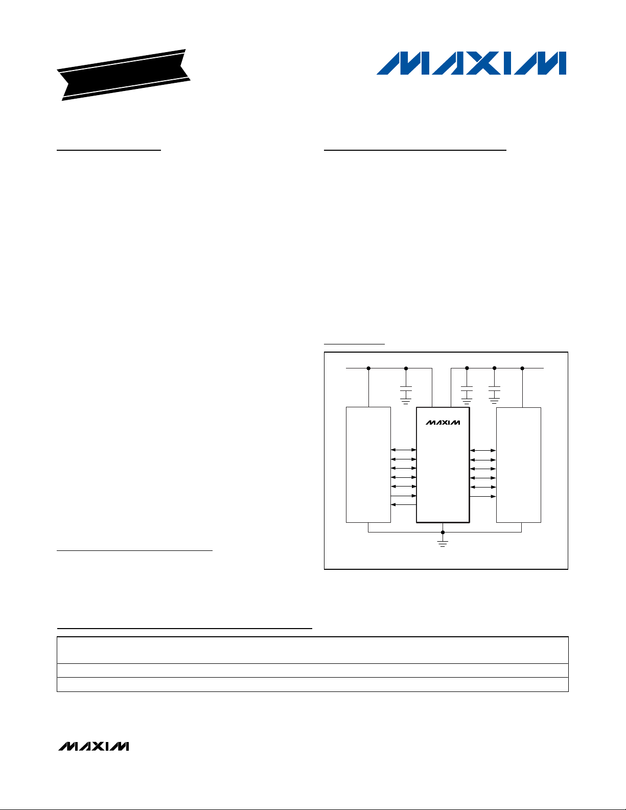
GND GND GND
+1.8V
SYSTEM
CONTROLLER
+3.3V
SD CARD
V
L
V
CC
CLK_RET
CLK_V
CC
CLOCK_IN
+3.3V
+1.8V
CLK_V
L
0.1μF
1μF
0.1μF
MAX13035E
DAT3
DAT2
DAT1
DAT0
CMD
CLOCK
I/O V
L_
I/O V
L_
I/O V
L_
I/O V
L_
I/O V
L_
I/O V
CC_
I/O V
CC_
I/O V
CC_
I/O V
CC_
I/O V
CC_
DAT3
DAT2
DAT1
DAT0
CMD
CLOCK
Typical Operating Circuits
Functional Diagram and Pin Configurations appear at end
of data sheet.
Typical Operating Circuits continued at end of data sheet.
Note: All devices are specified over the -40°C to +85°C operating
temperature range.
+
Denotes a lead-free package.
**
EP = Exposed paddle.
Ordering Information/Selector guide continued at end of
data sheet.
PART PIN-PACKAGE
MAX13030EEBE+ 16 UCSP High impedance High impedance B16-1
MAX13030EETE+ 16 TQFN-EP** High impedance High impedance T1644-4
I/O V
STATE DURING
L_
SHUTDOWN
I/O VCC_ STATE DURING
SHUTDOWN
PKG CODE
Page 2
MAX13030E–MAX13035E
6-Channel High-Speed Logic-Level Translators
2 _______________________________________________________________________________________
ABSOLUTE MAXIMUM RATINGS
Stresses beyond those listed under “Absolute Maximum Ratings” may cause permanent damage to the device. These are stress ratings only, and functional
operation of the device at these or any other conditions beyond those indicated in the operational sections of the specifications is not implied. Exposure to
absolute maximum rating conditions for extended periods may affect device reliability.
(All voltages referenced to GND.)
V
CC
, VL.....................................................................-0.3V to +4V
I/O V
CC_
, CLK_VCC....................................-0.3V to (VCC+ 0.3V)
I/O V
L_
, CLK_VL, CLK_RET ..........................-0.3V to (VL+ 0.3V)
EN.............................................................................-0.3V to +4V
Short-Circuit Duration I/O V
L_
, I/O V
CC_
,
CLK_V
CC
, CLK_VL, CLK_RET to GND.......................Continuous
Continuous Power Dissipation (T
A
= +70°C)
16-Bump UCSP (derate 8.2mW/°C)..............................660mW
16-Pin TQFN (derate 25.0mW/°C)...............................2000mW
Operating Temperature Range ...........................-40°C to +85°C
Storage Temperature Range .............................-65°C to +150°C
Junction Temperature......................................................+150°C
Bump Temperature (soldering)........................................+235°C
Lead Temperature (soldering, 10s) .................................+300°C
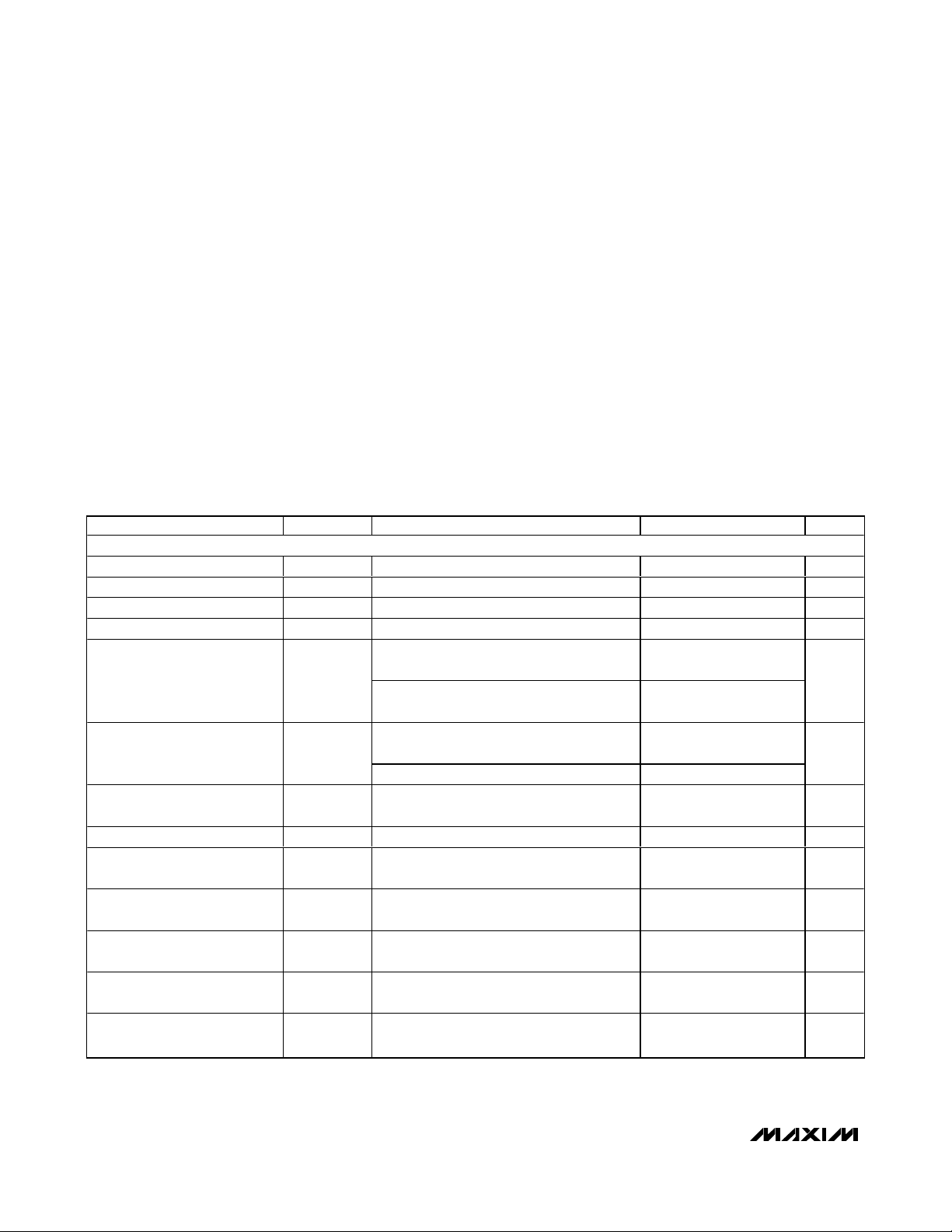
ELECTRICAL CHARACTERISTICS
(VCC= +2.2V to +3.6V, VL= +1.62V to +3.2V, EN = VL, TA= -40°C to +85°C, unless otherwise noted. Typical values are at VCC=
+3.3V, V
L
= +1.8V and TA= +25°C.) (Notes 1, 2)
PARAMETER SYMBOL CONDITIONS MIN TYP MAX UNITS
POWER SUPPLIES
VL Supply Range V
VCC Supply Range V
Supply Current from V
Supply Current from V
CC
L
VCC Shutdown Supply Current I
VL Shutdown Supply Current I
I/O V
, I/O VL_, CLK_V
CC_
CC
Tri-State Leakage Current
EN Input Leakage Current I
VL - VCC Shutdown Threshold
High
VL - VCC Shutdown Threshold
Low
I/O V
Pulldown Resistance
CC_
During Shutdown
I/O V
Pullup Resistance
CC_
During Shutdown
I/O VL_ Pulldown Resistance
During Shutdown
I
QVCC
I
SHDN-VCC
SHDN-VL
I
LEAK
LEAK_ENTA
V
V
R
VCC_PD_SD
R
VCC_PU_SD
R
VL_PD_SD
L
CC
QVL
TH_H
TH_L
(Note 2) 1.62 3.20 V
I/O VCC_ = VCC, I/O VL_ = V
I/O VCC_ = VCC, I/O VL_ = V
TA = +25°C, EN = GND or VL > VCC + 0.7V,
MAX13030E–MAX13034E
TA = +25°C, VL > VCC + 0.7V,
MAX13035E,
TA = +25°C, EN = GND or VL > VCC + 0.7V,
MAX13030E–MAX13034E
TA = +25°C, VL > VCC + 0.7V, MAX13035E 0.1 4
TA = +25°C, EN = GND or VL > VCC + 0.7V 0.1 2 µA
= +25°C, MAX13030E–MAX13034E 1 µA
VCC rising -0.2 0.05V
VCC falling -0.2 0.1V
EN = GND, MAX13032E/MAX13034E 10 16.5 23 kΩ
EN = GND, MAX13031E 10 16.5 23 kΩ
EN = GND, MAX13033E/MAX13034E 10 16.5 23 kΩ
2.2 3.6 V
L
L
16 25 µA
610µA
24
24
0.1 4
0.7 V
L
0.7 V
L
µA
µA
Page 3
MAX13030E–MAX13035E
6-Channel High-Speed Logic-Level Translators
_______________________________________________________________________________________ 3
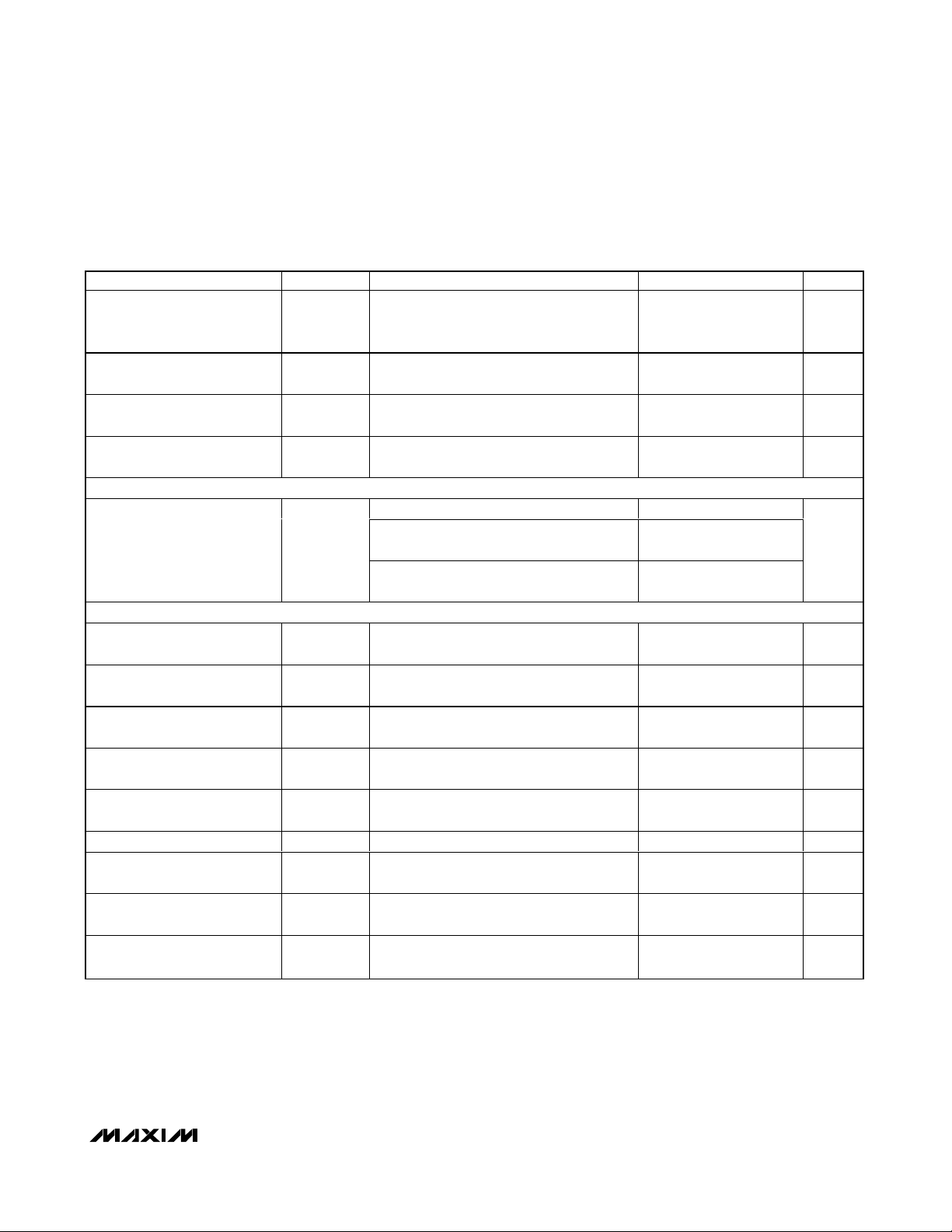
ELECTRICAL CHARACTERISTICS (continued)
(VCC= +2.2V to +3.6V, VL= +1.62V to +3.2V, EN = VL, TA= -40°C to +85°C, unless otherwise noted. Typical values are at VCC=
+3.3V, V
L
= 1.8V and TA= +25°C.) (Notes 1, 2)
PARAMETER SYMBOL CONDITIONS MIN TYP MAX UNITS
I/O VL_, CLK_VL, CLK_RET
Pullup Resistance During
Shutdown
I/O VL_, CLK_VL, CLK_RET
Pullup Current
I/O V
, CLK_VCC Pullup
CC_
Current
I/O VL to I/O VCC DC
Resistance
ESD PROTECTION (Note 3)
I/O V
CC_
, CLK_V
CC
LOGIC-LEVEL THRESHOLDS
I/O V
CLK_VL Input-Voltage
L_,
High Threshold
I/O V
CLK_VL Input-Voltage
L_,
Low Threshold
I/O V
, CLK_VCC Input-
CC_
Voltage High Threshold
I/O V
, CLK_VCC Input-
CC_
Voltage Low Threshold
EN Input-Voltage High
Threshold
EN Input-Voltage Low
I/O VL_, CLK_VL, CLK_RET
Output-Voltage High
I/O V
, CLK_V
L_
, CLK_RET
L
Output-Voltage Low
I/O VCC_, CLK_VCC OutputVoltage High
R
VL_PU_SD(VL
R
VL_PU
R
VCC_PU
R
IOVL_IOVCC
V
IHL
V
ILL
V
IHC
V
ILC
V
IH
V
IL
V
OHL
V
OLL
V
OHC
> VCC + 0.7V), MAX13035E 45 75 105 kΩ
EN = VCC or VL, I/O VL_ = GND 20 µA
EN = VCC or VL, I/O V
= GND 20 µA
CC_
(Note 3) 3 kΩ
Human Body Model, C
IEC 61000-4-2 Air-Gap Discharge,
C
= 1.0µF
VCC
IEC 61000-4-2 Contact Discharge,
= 1.0µF
C
VCC
(Note 4)
= 1.0µF ±15
VCC
±12
±8
V
0.2
kV
-
L
V
(Note 4) 0.15 V
(Note 4)
CC
0.4
V
V
-
(Note 4) 0.2 V
V
-
MAX13030E–MAX13034E
0.4
L
V
MAX13030E–MAX13034E 0.4 V
I/O VL_, CLK_VL, CLK_RET source current
= 20µA, I/O V
I/O V
, CLK_V
L_
20µA, I/O V
_ ≥ VCC - 0.4V
CC
, CLK_RET sink current =
L
_ ≤ 0.2V
CC
I/O VCC_, CLK_VCC source current = 20µA,
I/O V
_ ≥ VL - 0.2V
L
2/3 V
2/3
V
CC
L
1/3 V
V
V
L
V
Page 4
MAX13030E–MAX13035E
6-Channel High-Speed Logic-Level Translators
4 _______________________________________________________________________________________
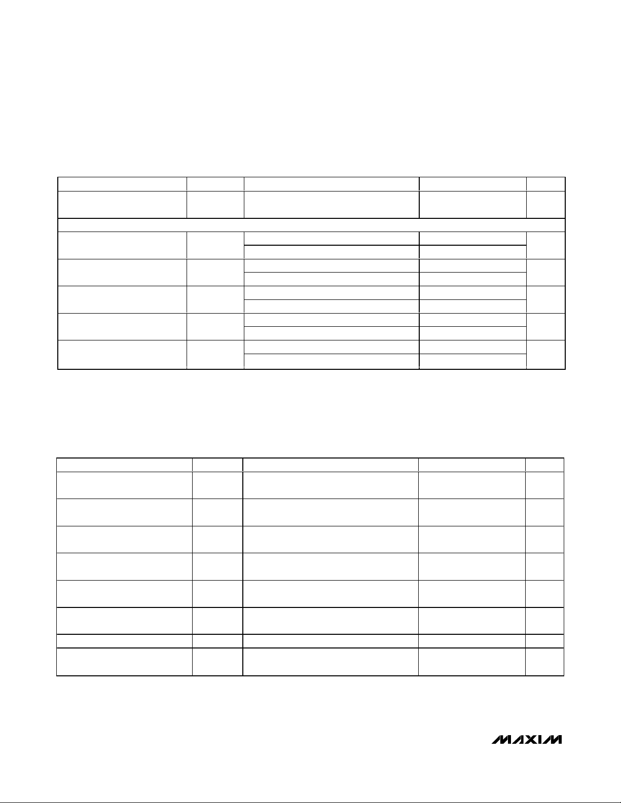
ELECTRICAL CHARACTERISTICS (continued)
(VCC= +2.2V to +3.6V, VL= +1.62V to +3.2V, EN = VL, TA= -40°C to +85°C, unless otherwise noted. Typical values are at VCC=
+3.3V, V
L
= 1.8V and TA= +25°C.) (Notes 1, 2)
TIMING CHARACTERISTICS
(VCC= +2.2V to +3.6V, VL= +1.62V to +3.2V, C
I/OVL
≤ 15pF, C
I/OVCC
≤ 15pF, R
SOURCE
= 150Ω, EN = VL, I/O VL_to I/O V
CC_
rise/fall time = 3ns, TA= -40°C to +85°C, unless otherwise noted. Typical values are at VCC= +3.3V, VL= 1.8V and TA= +25°C.)
(Note 1)
PARAMETER SYMBOL CONDITIONS MIN TYP MAX UNITS
I/O V
Voltage Low
, CLK_VCC Output-
CC_
V
OLC
I/O V
I/O V
RISE/FALL TIME ACCELERATOR STAGE (Note 3)
Accelerator Pulse Duration
VL-Output-Accelerator Source
Impedance
VCC-Output-Accelerator Source
Impedance
VL-Output-Accelerator Sink
Impedance
VCC-Output-Accelerator Sink
Impedance
On falling edge 3
On rising edge 3
VL = 1.62V 11
V
L
VCC = 2.2V 9
V
CC
VL = 1.62V 9
V
L
VCC = 2.2V 10
V
CC
, CLK_VCC sink current = 20µA,
CC_
_ ≤ 0.15V
L
= 3.2V 6
= 3.6V 8
= 3.2V 8
= 3.6V 9
1/3
V
CC
I/O VCC_, CLK_VCC Rise Time t
I/O VCC_, CLK_VCC Fall Time t
I/O VL_, CLK_VL Rise Time t
I/O VL_, CLK_VL Fall Time t
Propagation Delay
(Driving I/O V
Propagation Delay
(Driving I/O V
Channel-to-Channel Skew t
Propagation Delay from
I/O V
PARAMETER SYMBOL CONDITIONS MIN TYP MAX UNITS
RVCC
FVCC
RVL
FVL
t
PVL-VCC
t
PVCC-VL
SKEW
t
EN-VCC
to I/O V
L_
_, CLK_VL)
L
_, CLK_VCC)
CC
after EN
CC_
RS = 150Ω, C
I/OVCC
= 10pF, C
10pF, push-pull drivers (Figure 1)
RS = 150Ω, C
I /OV C C
= 10p F, C
10p F ( Figures 1, 2)
RS = 150Ω, C
I /OV L
= 15p F, C
push-pull drivers (Figure 3)
RS = 150Ω, C
I /OV L
= 15p F, C
( Figures 3, 4)
RS = 150Ω, C
I/OVCC
= 10pF, C
10pF, push-pull drivers (Figure 1)
RS = 150Ω, C
I /OV L
= 15p F, C
push-pull drivers (Figure 3)
RS = 150Ω, C
R
= 1MΩ, C
LOAD
I /OV C C
I/OVCC
= 10p F, C
= 10pF (Figure 5)
(MAX13030E–MAX13034E)
CLK_VCC
C LK _V C C
C LK _V L
C LK _V L
CLK_VCC
C LK _V L
I /OV L
=
=
= 15p F,
= 15p F
=
= 15p F,
= 15p F 0.8 ns
5µs
2.5 ns
2.5 ns
2.5 ns
2.5 ns
6.5 ns
6.5 ns
V
ns
Ω
Ω
Ω
Ω
Page 5
MAX13030E–MAX13035E
6-Channel High-Speed Logic-Level Translators
_______________________________________________________________________________________ 5
TIMING CHARACTERISTICS (continued)
(VCC= +2.2V to +3.6V, VL= +1.62V to +3.2V, C
I/OVL
≤ 15pF, C
I/OVCC
≤ 15pF, R
SOURCE
= 150Ω, EN = VL, I/O VL_to I/O V
CC_
rise/fall time = 3ns, TA= -40°C to +85°C, unless otherwise noted. Typical values are at VCC= +3.3V, VL= 1.8V and TA= +25°C.)
(Note 1)
Note 1: All units are 100% production tested at T
A
= +25°C. Limits over the operating temperature range are guaranteed by design
and not production tested.
Note 2: V
L
must be less than or equal to VCC- 0.2V during normal operation. However, VLcan be greater than VCCduring startup
and shutdown conditions and the part will not latch-up or be damaged.
Note 3: Guaranteed by design.
Note 4: Input thresholds are referenced to the boost circuit.
Propagation Delay from
I/O V
Maximum Data Rate
PARAMETER SYMBOL CONDITIONS MIN TYP MAX UNITS
t
to I/O VL_ after EN
CC_
EN-VL
R
= 1MΩ, C
LOAD
(MAX13030E–MAX13034E)
Push-pull operation, R
C
C
I/OVCC_
CLK_VCC
= 10pF, C
= 10pF, C
= 15pF (Figure 5)
I/OVL
SOURCE
I/OVL_
CLK_VL
= 150_,
= 15pF,
= 15pF
5µs
100 Mbps
Page 6
MAX13030E–MAX13035E
6-Channel High-Speed Logic-Level Translators
6 _______________________________________________________________________________________
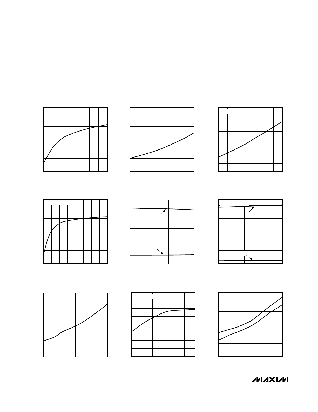
Typical Operating Characteristics
(VCC= 3.3V, VL= 1.8V, CL= 15pF, R
SOURCE
= 150Ω, data rate = 100Mbps, push-pull driver, TA= +25°C, unless otherwise noted.)
750
780
770
760
800
790
840
830
820
810
850
2.2 2.4 2.6 2.8 3.0 3.2 3.4 3.6
VL SUPPLY CURRENT vs. VCC SUPPLY
VOLTAGE (DRIVING I/O V
L_
, VL = 1.8V)
MAX13030E toc01
VCC SUPPLY VOLTAGE (V)
V
L
SUPPLY CURRENT (μA)
DRIVING ONE I/O V
L
0
2
1
4
3
6
5
7
9
8
10
1.6 2.0 2.21.8 2.4 2.6 2.8 3.0 3.2
VL SUPPLY CURRENT vs. VL SUPPLY
VOLTAGE (DRIVING I/O V
CC_
, VCC = 3.6V)
MAX13030E toc02
VL SUPPLY VOLTAGE (V)
V
L
SUPPLY CURRENT (mA)
DRIVING ONE I/O V
CC
5.0
10.0
7.5
15.0
12.5
22.5
20.0
17.5
25.0
2.2 2.62.4 2.8 3.0 3.2 3.4 3.6
VCC SUPPLY CURRENT vs. VCC SUPPLY
VOLTAGE (DRIVING I/O V
L_
, VL = 1.8V)
MAX13030E toc03
VCC SUPPLY VOLTAGE (V)
V
CC
SUPPLY CURRENT (mA)
DRIVING ONE I/O V
L
15.0
16.0
15.5
17.0
16.5
18.0
17.5
18.5
19.5
19.0
20.0
1.6 2.0 2.21.8 2.4 2.6 2.8 3.0 3.2
VCC SUPPLY CURRENT vs. VL SUPPLY
VOLTAGE (DRIVING I/O V
CC_
, VCC = 3.6V)
MAX13030E toc04
VL SUPPLY VOLTAGE (V)
V
CC
SUPPLY CURRENT (mA)
DRIVING ONE I/O V
CC
0
4
2
10
8
6
16
14
12
18
-40 10-15 35 60 85
SUPPLY CURRENT
vs. TEMPERATURE (DRIVING I/O V
CC_
)
MAX13030E toc05
TEMPERATURE (°C)
SUPPLY CURRENT (mA)
DRIVING ONE I/O V
CC
I
CC
I
L
0
6
4
2
8
10
12
14
16
18
20
-40 10-15 35 60 85
SUPPLY CURRENT
vs. TEMPERATURE (DRIVING I/O V
L_
)
MAX13030E toc06
TEMPERATURE (°C)
SUPPLY CURRENT (mA)
I
CC
I
L
DRIVING ONE I/O V
L
1.0
1.5
2.0
2.5
3.0
3.5
4.0
4.5
5.0
10 2015 25 30 35 40
VL SUPPLY CURRENT vs. CAPACITIVE
LOAD ON I/O V
L_
(DRIVING I/O V
CC_
)
MAX13030E toc07
CAPACITIVE LOAD (pF)
V
L
SUPPLY CURRENT (mA)
DRIVING ONE I/O V
CC
16.0
16.5
17.0
17.5
18.0
18.5
19.0
19.5
20.0
10 2015 25 30 35 40
VCC SUPPLY CURRENT vs. CAPACITIVE
LOAD ON I/O V
CC_
(DRIVING I/O VL_)
MAX13030E toc08
CAPACITIVE LOAD (pF)
V
CC
SUPPLY CURRENT (mA)
DRIVING ONE I/O V
L
500
800
700
600
900
1000
1100
1200
1300
1400
1500
10 2015 25 30 35 40
RISE/FALL TIME vs. CAPACITIVE
LOAD ON I/O V
CC_
(DRIVING I/O VL_)
MAX13030E toc09
CAPACITIVE LOAD (pF)
RISE/FALL TIME (ps)
t
RVCC
t
FVCC
Page 7

MAX13030E–MAX13035E
6-Channel High-Speed Logic-Level Translators
_______________________________________________________________________________________
7
Typical Operating Characteristics (continued)
(VCC= 3.3V, VL= 1.8V, CL= 15pF, R
SOURCE
= 150Ω, data rate = 100Mbps, push-pull driver, TA= +25°C, unless otherwise noted.)
RISE/FALL TIME vs. CAPACITIVE
LOAD ON I/O V
3000
2750
2500
2250
2000
1750
1500
RISE/FALL TIME (ps)
1250
1000
750
500
10 2015 25 30 35 40
CAPACITIVE LOAD (pF)
PROPAGATION DELAY vs. CAPACITIVE
LOAD ON I/O V
5.0
4.5
4.0
3.5
3.0
2.5
PROPAGATION DELAY (ns)
2.0
1.5
1.0
10 2015 25 30 35 40
CAPACITIVE LOAD (pF)
(DRIVING I/O V
L_
t
RVL
(DRIVING I/O V
L_
t
PHL
t
PLH
)
CC_
MAX13030E toc10
t
FVL
)
CC_
MAX13030E toc12
PROPAGATION DELAY vs. CAPACITIVE
LOAD ON I/O V
5.0
4.5
4.0
3.5
3.0
PROPAGATION DELAY (ns)
2.5
2.0
10 20 2515 30 35 40
(DRIVING I/O VL_)
CC_
t
PLH
t
PHL
CAPACITIVE LOAD (pF)
TYPICAL I/O VL_ DRIVING
(FREQUENCY = 26MHz, C
IOVCC
10ns/div
= 40pF)
MAX13030E toc13
MAX13030E toc11
I/O V
L_
1V/div
I/O V
CC_
2V/div
TYPICAL I/O V
(FREQUENCY = 26MHz, C
10ns/div
CC_
DRIVING
= 15pF)
IOVL
MAX13030E toc14
I/O V
2V/div
I/O V
1V/div
CC_
L_
TYPICAL CLK_ VL DRIVING
(FREQUENCY = 26MHz, C
10ns/div
CLK_VCC
= 40pF)
MAX13030E toc15
CLK_ V
1V/div
CLK_ V
2V/div
CLK_RET
1V/div
L
CC
Page 8

MAX13030E–MAX13035E
6-Channel High-Speed Logic-Level Translators
8 _______________________________________________________________________________________
Pin Description
PIN
MAX13030E–MAX13034E MAX13035E
UCSP TQFN UCSP TQFN
A1 4 A1 4 I/O VL3 Input/Output 3. Referenced to VL.
A2 6 A2 6 I/O VCC3 Input/Output 3. Referenced to VCC.
A3 7 A3 7 I/O VCC4 Input/Output 4. Referenced to VCC.
A4 9 A4 9 I/O VL4 Input/Output 4. Referenced to VL.
B1 3 B1 3 I/O VL2 Input/Output 2. Referenced to VL.
B2 5 B2 5 I/O VCC2 Input/Output 2. Referenced to VCC.
B3 8 B3 8 I/O VCC5 Input/Output 5. Referenced to VCC.
B4 10 B4 10 I/O VL5 Input/Output 5. Referenced to VL.
C1 2 C1 2 V
C2 16 C2 16 V
C3 13 C3 13 GND Ground
C4 11 — — EN
D1 1 D1 1 I/O VL1 Input/Output 1. Referenced to VL.
D2 15 D2 15 I/O VCC1 Input/Output 1. Referenced to VCC.
D3 14 — — I/O VCC6 Input/Output 6. Referenced to VCC.
D4 12 — — I/O VL6 Input/Output 6. Referenced to VL.
— — C4 11 CLK_RET
— — D3 14 CLK_V
— — D4 12 CLK_VLTranslator Channel for a Clock Applied to V
— EP — EP EP Exposed Paddle. Connect exposed paddle to GND.
NAME FUNCTION
L
CC
CC
Logic-Supply Voltage, +1.62V to +3.2V. Bypass VL to GND with
a 0.1µF capacitor placed as close as possible to the device.
Power-Supply Voltage, +2.2V to +3.6V. Bypass VCC to GND with
a 0.1µF ceramic capacitor. For full ESD protection, connect a
1µF ceramic capacitor from V
the V
input.
CC
Enable Input. Drive EN to GND for shutdown mode, or drive EN to
or VCC for normal operation.
V
L
Clock Return Output. CLK_RET is the returned signal of a clock
applied to CLK_V
Translator Channel for a Clock Applied to V
. CLK_RET is referenced to VL.
L
to GND as close as possible to
CC
CC
L
Page 9

MAX13030E–MAX13035E
6-Channel High-Speed Logic-Level Translators
_______________________________________________________________________________________ 9
Test Circuits/Timing Diagrams
Figure 1. Push-Pull Driving I/O VL_Test Circuit and Timing
Figure 2. Open-Drain Driving I/O VL_ Test Circuit and Timing
V
L
V
CC
V
CC
I/O V
L_
(CLK_VL*)
V
L
V
L
EN**
MAX13030E–
MAX13035E
150Ω
*MAX13035E ONLY
**MAX13030E–MAX13034E ONLY
V
L
EN**
V
L
MAX13030E–
MAX13035E
V
L
I/O V
L_
(CLK_VL*)
V
GATE
V
CC
V
CC
I/O V
CC_
(CLK_VCC*)
I/O V
CC_
(CLK_VCC*)
t
V
CC
RVCC
90%
I/O V
L
50%
50%
I/O V
10%
CC
C
(C
CLK_VCC
*)
t
PLH
t
= t
RVCC
PLH
OR t
PHL
I/O V
CC
PVL-VCC
t
IOVCC
V
CC
90%
V
GATE
50%
50%
10%
C
(C
CLK_VCC
*)
IOVCC
90%
50%
t
PHL
90%
50%
t
FVCC
t
FVCC
50%
10%
50%
10%
*MAX13035E ONLY
**MAX13030E–MAX13034E ONLY
t
PLH
t
PVL-VCC
t
PHL
= t
PHL
Page 10

MAX13030E–MAX13035E
6-Channel High-Speed Logic-Level Translators
10 ______________________________________________________________________________________
Test Circuits/Timing Diagrams (continued)
Figure 3. Push-Pull Driving I/O V
CC_
Test Circuit and Timing
Figure 4. Open-Drain Driving I/O V
CC_
Test Circuit and Timing
50%
t
FVL
90%
50%
10%
I/O V
t
PHL
(C
C
CLK_VL
IOVL
V
L
I/O V
L_
(CLK_VL*)
*)
*MAX13035E ONLY
V
L
V
L
EN**
MAX13030E–
MAX13035E
V
V
**MAX13030E–MAX13034E ONLY
t
10%
t
PLH
t
PVCC-VL
RVL
I/O V
CC
90%
50%
= t
OR t
PLH
PHL
V
CC
CC
CC
50%
I/O V
CC_
(CLK_VCC*)
150Ω
L
V
CLK_VL
*)
*)
I/O V
L_
(CLK_VL*)
L
(C
C
IOVL
(C
CLK_VL
*MAX13035E ONLY
EN**
V
L
MAX13030E–
MAX13035E
V
L
**MAX13030E–MAX13034E ONLY
V
V
CC
V
CC
I/O V
CC_
(CLK_VCC*)
t
CC
RVL
I/O V
90%
50%
50%
50%
10%
V
GATE
t
PLH
t
PVCC-VL
= t
PHL
t
FVL
L
90%
50%
10%
t
PHL
Page 11

MAX13030E–MAX13035E
6-Channel High-Speed Logic-Level Translators
______________________________________________________________________________________ 11
Test Circuits/Timing Diagrams (continued)
Figure 5. Enable Test Circuit and Timing
SOURCE
SOURCE
V
EN-VCC
0
V
0
V
0
AND t"
L
L
CC
V
0
V
0
V
0
L
L
CC
EN-VCC
.
EN
I/O V
I/O V
CC_
EN
L_
t'
EN-VCC
V
/ 2
CC
MAX13030E–
V
L
MAX13034E
I/O V
L_
V
L
V
CC
I/O V
CC_
C
R
LOAD
V
CC
IOVCC
EN
MAX13030E–
V
L
R
V
CC
LOAD
EN
t"
EN-VCC
MAX13034E
I/O V
L_
I/O V
CC_
C
IOVCC
I/O V
L_
I/O V
CC_
t
IS WHICHEVER IS LARGER BETWEEN t'
EN-VCC
V
/ 2
CC
EN
V
MAX13030E–
L
SOURCE
I/O V
L_
C
LOAD
IOVL
R
MAX13034E
EN
MAX13030E–
V
L
MAX13034E
SOURCE
I/O V
V
L
R
LOAD
L_
C
IOVL
V
L
I/O V
I/O V
I/O V
CC_
CC_
EN
t'
EN-VL
0
V
CC
0
V
L_
EN
VL / 2
t"
EN-VL
L
0
V
L
0
V
CC
V
CC
I/O V
CC_
V
CC
V
CC
0
I/O V
CC_
I/O V
L_
t
IS WHICHEVER IS LARGER BETWEEN t'
EN-VCC
VL / 2
EN-VCC
AND t"
V
L
0
EN-VCC
.
Page 12

MAX13030E–MAX13035E
Detailed Description
The MAX13030E–MAX13035E 6-channel, bidirectional
level translators provide the level shifting necessary for
100Mbps data transfer in multivoltage systems. The
MAX13030E–MAX13035E are ideally suited for memory
card level translation, as well as generic level translation
in systems with six channels. Externally applied voltages, V
CC
and VL, set the logic levels on either side of
the device. Logic signals present on the VLside of the
device appear as a higher voltage logic signal on the
VCCside of the device, and vice versa. The MAX13035E
features a CLK_RET output that returns the same clock
signal applied to the CLK_VL input.
The MAX13030E–MAX13035E operate at full speed
with external drivers that source as little as 4mA output
current. Each I/O channel is pulled up to VCCor VLby
an internal 30µA current source, allowing the
MAX13030E–MAX13035E to be driven by either pushpull or open-drain drivers.
The MAX13030E–MAX13034E feature an enable (EN)
input that places the device into a low-power shutdown
mode when driven low. The MAX13030E–MAX13035E
features an automatic shutdown mode that disables the
part when V
CC
is less than VL. The state of I/O V
CC_
and
I/O VL_during shutdown is chosen by selecting the
appropriate part version (see
Ordering Information/
Selector Guide
).
The MAX13030E–MAX13035E accept VCCvoltages from
+2.2V to +3.6V and VLvoltages from +1.62V to +3.2V.
Level Translation
For proper operation, ensure that +2.2V ≤ VCC≤ +3.6V,
and +1.62V ≤ VL≤ VCC- 0.2V. When power is supplied to
V
L
while VCCis either missing or less than VL,
the MAX13030E–MAX13035E automatically enters a
low- power mode. In addition, the MAX13030E–
MAX13034E enters a low-power mode if EN = 0V. This
allows V
CC
to be disconnected and still have a known
state on I/O VL_. The maximum data rate depends heavily
on the load capacitance (see the
Typical Operating
Characteristics Rise/Fall Times
), output impedance of the
driver, and the operating voltage range.
Input Driver Requirements
The MAX13030E–MAX13035E architecture is based on
an nMOS pass gate and output accelerator stages (see
Figure 6). Output accelerator stages are always in tristate mode except when there is a transition on any of
the translators on the input side, either I/O VL_, CLK_VL,
I/O V
CC_
, or CLK_VCC. A short pulse is then generated
during which the output accelerator stages become
active and charge/discharge the capacitances at the
I/Os. Due to its architecture, both input stages become
active during the one-shot pulse. This can lead to some
current feeding into the external source that is driving the
translator. However, this behavior helps to speed up the
transition on the driven side.
The MAX13030E–MAX13035E have internal current
sources capable of sourcing 30µA to pullup the I/O
lines. These internal pullup current sources allow the
inputs to be driven with open-drain drivers, as well as
push-pull drivers. It is not recommended to use external pullup resistors on the I/O lines. The architecture of
the MAX13030E–MAX13035E permit either side to be
driven with a minimum of 4mA drivers or larger.
Output Load Requirements
The MAX13030E–MAX13035E I/O are designed to drive
CMOS inputs. Do not load the I/O lines with a resistive
load less than 25kΩ and do not place an RC circuit at
the input of these devices to slow down the edges. If a
slower rise/fall time is required, refer to the MAX3000E/
MAX3001E logic-level translator datasheet. For I2C
level translation, refer to the MAX3372E–MAX3379E/
MAX3390E–MAX3393E datasheet.
Shutdown Mode
The MAX13030E–MAX13034E feature an enable (EN)
input that places the device into a low-power shutdown
mode when driven low. The MAX13030E–MAX13035E
features an automatic shutdown mode that disables the
part when VCCis missing or less than VL.
6-Channel High-Speed Logic-Level Translators
12 ______________________________________________________________________________________
Figure 6. Simplified Functional Diagram for One I/O Line
ENABLE
V
I/O V
CC
V
L
ENABLE
ENABLE
30μA
I/O V
L_
BOOST
CIRCUIT
BOOST
CIRCUIT
V
CC
V
CC
<
VCC - 0.2V
L
V
L
V
L
NOTES: 1) THE MAX13030E–MAX13034E ARE ENABLED WHEN
V
2) THE MAX13035E IS ENABLED WHEN V
<
VCC - 0.2V
L
AND EN = VL.
30μA
.
CC_
Page 13

Clock Return (CLK_RET)
The MAX13035E features a CLK_RET output that returns
the clock signal applied to CLK_V
L
. CLK_VLand
CLK_VCCare identical to the other I/O channels, the only
difference being that CLK_VCCis internally tied to the
VCCside of CLK_RET (see the
Functional Diagram
).
Application Information
Layout Recommendations
Use standard high-speed layout practices when laying
out a board with the MAX13030E–MAX13035E. For
example, to minimize line coupling, place all other signal
lines not connected to the MAX13030E–MAX13035E at
least 1x the substrate height of the PCB away from the
input and output lines of the MAX13030E–MAX13035E.
Power-Supply Decoupling
To reduce ripple and the chance of introducing data
errors, bypass VLand VCCto ground with 0.1µF ceramic capacitors. Place all capacitors as close as possible
to the power-supply inputs. For full ESD protection,
bypass VCCwith a 1µF ceramic capacitor located as
close as possible to the VCCinput.
Unidirectional vs. Bidirectional Level
Translator
The MAX13030E–MAX13035E bidirectional level translators can operate as a unidirectional device to translate signals without inversion. These devices provide
the smallest solution (UCSP package) for unidirectional
level translation without inversion.
Use with External Pullup/Pulldown
Resistors
Due to the architecture of the MAX13030E–
MAX13035E, it is not recommended to use external
pullup or pulldown resistors on the bus. In certain applications, the use of external pullup or pulldown resistors
is desired to have a known bus state when there is no
active driver on the bus. For example, this may happen
when interfacing to a memory card slot with no memory
card inserted. The MAX13030E–MAX13035E include
internal pullup current sources that set the bus state
when the device is enabled. In shutdown mode,
the state of I/O V
CC_
and I/O V
L_
is dependent on
the selected part version (see
Ordering Information/
Selector Guide
for further information).
Open-Drain Signaling
The MAX13030E–MAX13035E are designed to pass
open-drain as well as CMOS push-pull signals. When
used with open-drain signaling, the rise time is dominated by the interaction of the internal pullup current
source and the parasitic load capacitance. The
MAX13030E–MAX13035E include internal rise time
accelerators to speed up transitions, eliminating any
need for external pullup resistors.
SD Card Detection
SD, MiniSD, MMC and similar types of cards provide
detection of a card through a pullup resistor on one of
the DAT lines, or by use of a mechanical switch. This
pullup resistor is internal to the memory card itself. The
MAX13030E–MAX13035E only support detection of
a memory card through a mechanical switch, and it
is recommended that the internal resistor for card
detection be switched off by the command interface.
For example, when using SD cards, the command
SET_CLR_CARD_DETECT (ACMD42) disables this
resistor.
UCSP Applications Information
For the latest application details on UCSP construction,
dimensions, tape carrier information, PCB techniques,
bump-pad layout, and recommended reflow temperature profiles, as well as the latest information on reliability testing results, go to Maxim’s web site at
www.maxim-ic.com/ucsp to find the Application Note:
UCSP – A Wafer-Level Chip-Scale Package.
Chip Information
Process: BiCMOS
MAX13030E–MAX13035E
6-Channel High-Speed Logic-Level Translators
______________________________________________________________________________________ 13
Page 14

MAX13030E–MAX13035E
6-Channel High-Speed Logic-Level Translators
14 ______________________________________________________________________________________
Functional Diagram
V
L
V
CC
V
L
V
CC
MAX13030E–
MAX13034E
I/O V
I/O V
1
1
L
L
2
I/O V
L
I/O VL3
I/O V
4
I/O V
L
5
L
I/O V
I/O V
I/O VCC3
I/O V
I/O V
MAX13035E
I/O VL1
1
CC
I/O VL2
2
CC
I/O VL3
I/O V
I/O V
4
L
5
L
4
CC
5
CC
I/O V
CC
I/O V
CC
I/O VCC3
I/O V
CC
I/O V
CC
1
2
4
5
I/O V
6
L
EN
GND
I/O V
CC
L
CLK_RET
GND
CLK_ V
6
CLK_ V
CC
Page 15

MAX13030E–MAX13035E
6-Channel High-Speed Logic-Level Translators
______________________________________________________________________________________ 15
Pin Configurations
TOP VIEW
6
L
EN
I/O V
12 11 10 9
GND
13
I/O V
6
CC
14
MAX13030E–
I/O VCC1
V
15
16
CC
+
MAX13034E
*EP
1234
L
1
L
V
I/O V
16 TQFN (4mm x 4mm)
*CONNECT EXPOSED PADDLE TO GROUND
TOP VIEW
CLK_VLCLK_RET
12 11 10 9
GND
13
CLK_V
CC
14
I/O VCC1
V
15
16
CC
+
MAX13035E
*EP
1234
L
1
L
V
I/O V
16 TQFN (4mm x 4mm)
*CONNECT EXPOSED PADDLE TO GROUND
5
I/O V
2
I/O V
5
L
I/O V
2
L
I/O V
4
L
L
I/O V
TOP VIEW
(BUMPS ON BOTTOM)
I/O V
8
CC
I/O V
7
CC
I/O V
6
CC
I/O VCC2
5
12 3
+
A
5
4
3
I/O V
B
I/O V
MAX13030E–MAX13034E
3
I/O VCC3
L
2
I/O VCC2
L
I/O VCC4
I/O VCC5
I/O V
I/O V
4
4
L
5
L
C
V
I/O V
L
L
3
L
L
I/O V
D
V
CC
1
I/O VCC1
GND
I/O V
EN
6
I/O V
CC
6
L
16 UCSP (2mm x 2mm)
4
L
I/O V
3
L
I/O V
8
7
6
5
TOP VIEW
(BUMPS ON BOTTOM)
I/O V
5
CC
4
I/O V
CC
I/O V
3
CC
I/O VCC2
12 3
+
A
I/O V
3
L
B
I/O V
2
L
C
V
L
D
I/O VL1
I/O VCC3
I/O VCC2
V
CC
I/O VCC1
MAX13035E
I/O VCC4
I/O VCC5
GND
CLK_V
4
I/O V
4
L
I/O V
5
L
CLK_RET
CLK_V
CC
L
16 UCSP (2mm x 2mm)
Page 16

MAX13030E–MAX13035E
6-Channel High-Speed Logic-Level Translators
16 ______________________________________________________________________________________
Typical Operating Circuits (continued)
Ordering Information/Selector Guide (continued)
Note: All devices are specified over the -40°C to +85°C operating
temperature range.
+
Denotes a lead-free package.
**
EP = Exposed paddle.
+1.8V
0.1μF
+1.8V
SYSTEM
CONTROLLER
EN
DATA
GND GND GND
EN
I/O V
6
PART PIN-PACKAGE
MAX13031EEBE+* 16 UCSP High impedance 16.5kΩ to V
MAX13031EETE+* 16 TQFN-EP** High impedance 16.5kΩ to V
MAX13032EEBE+ 16 UCSP High impedance 16.5kΩ to GND B16-1
MAX13032EETE+ 16 TQFN-EP** High impedance 16.5kΩ to GND T1644-4
MAX13033EEBE+* 16 UCSP 16.5kΩ to GND High impedance B16-1
MAX13033EETE+* 16 TQFN-EP** 16.5kΩ to GND High impedance T1644-4
MAX13034EEBE+* 16 UCSP 16.5kΩ to GND 16.5kΩ to GND B16-1
MAX13034EETE+* 16 TQFN-EP** 16.5kΩ to GND 16.5kΩ to GND T1644-4
MAX13035EEBE+ 16 UCSP 75kΩ to V
MAX13035EETE+ 16 TQFN-EP** 75kΩ to V
I/O V
L_
STATE DURING
SHUTDOWN
V
V
L
CC
MAX13030E–
MAX13034E
I/O V
L_
L
L
CC_
+3.3V
0.1μF
1μF
+3.3V
SYSTEM
DATA
6
I/O VCC_ STATE DURING
SHUTDOWN
High impedance B16-1
High impedance T1644-4
CC
CC
PKG CODE
B16-1
T1644-4
Page 17

MAX13030E–MAX13035E
6-Channel High-Speed Logic-Level Translators
______________________________________________________________________________________ 17
Package Information
(The package drawing(s) in this data sheet may not reflect the most current specifications. For the latest package outline information,
go to www.maxim-ic.com/packages
.)
16L,UCSP.EPS
PACKAGE OUTLINE, 4x4 UCSP
21-0101
1
H
1
Page 18

MAX13030E–MAX13035E
6-Channel High-Speed Logic-Level Translators
Maxim cannot assume responsibility for use of any circuitry other than circuitry entirely embodied in a Maxim product. No circuit patent licenses are
implied. Maxim reserves the right to change the circuitry and specifications without notice at any time.
18
____________________Maxim Integrated Products, 120 San Gabriel Drive, Sunnyvale, CA 94086 408-737-7600
© 2007 Maxim Integrated Products is a registered trademark of Maxim Integrated Products, Inc.
Boblet
Package Information (continued)
(The package drawing(s) in this data sheet may not reflect the most current specifications. For the latest package outline information,
go to www.maxim-ic.com/packages
.)
24L QFN THIN.EPS
PACKAGE OUTLINE,
12, 16, 20, 24, 28L THIN QFN, 4x4x0.8mm
21-0139
PACKAGE OUTLINE,
12, 16, 20, 24, 28L THIN QFN, 4x4x0.8mm
21-0139
1
E
2
2
E
2
 Loading...