

Page 1
General Description
The MAX13020/MAX13021 ±60V fault-protected lowpower local interconnect network (LIN) transceivers are
ideal for use in automotive network applications where
high reliability is required. The devices provide the
interface between the LIN master/slave protocol controller, and the physical bus described in the LIN 2.0
specification package and SAE J2602 specification.
The devices are intended for in-vehicle subnetworks
with a single master and multiple slaves.
The extended fault-protected voltage range of ±60V on
the LIN bus line allows for use in +12V, +24V, and
+42V automotive applications. The devices allow communication up to 20kbaud, and include slew-rate limited transmitters for enhanced electromagnetic
emissions (EME) performance. The devices feature a
low-power 4µA sleep mode and provide wake-up
source detection.
The MAX13020 is a pin-to-pin replacement and is functionally compatible with the Philips TJA1020. The
MAX13021 includes enhanced bus dominant clamping
fault management for reduced quiescent current during
LIN bus shorts to GND. The MAX13020/MAX13021 are
available in the 8-pin SO package, and operate over
the -40°C to +125°C automotive temperature range.
Applications
+12V/+42V Automotive
+24V Heavy Truck and Bus
Features
♦ MAX13020 is a Pin-to-Pin Upgrade for TJA1020
♦ ESD Protection
±12kV Human Body Model (LIN)
±4kV Contact Discharge (LIN, NWAKE, BAT)
♦ LIN 2.0/SAE J2602 Compatible
♦ Slew-Rate Limited Transmitter for Low
Electromagnetic Emissions (EME)
♦ Robust Electromagnetic Immunity (EMI)
♦ Passive Behavior in Unpowered State
♦ TXD Dominant Timeout Function
♦ LIN Bus Dominant Management (MAX13021 Only)
♦ Input Levels Compatible with +3.3V and +5V
Controllers
♦ Integrated 30kΩ Termination Resistor for Slave
Applications
♦ Low 4µA Sleep Mode with Local and Remote
Wake-Up Detection
♦ Wake-Up Source Recognition
♦ Thermal Shutdown
MAX13020/MAX13021
±60V Fault-Protected LIN Transceivers
________________________________________________________________ Maxim Integrated Products 1
19-0559; Rev 1; 6/06
For pricing, delivery, and ordering information, please contact Maxim/Dallas Direct! at
1-888-629-4642, or visit Maxim’s website at www.maxim-ic.com.
Ordering Information
PART
L IN B U S
D O M IN A N T
PIN-
PACKAGE
CODE
MAX13020ASA+
— 8 SO S8-5
MAX13021ASA+
Yes 8 SO S8-5
BAT
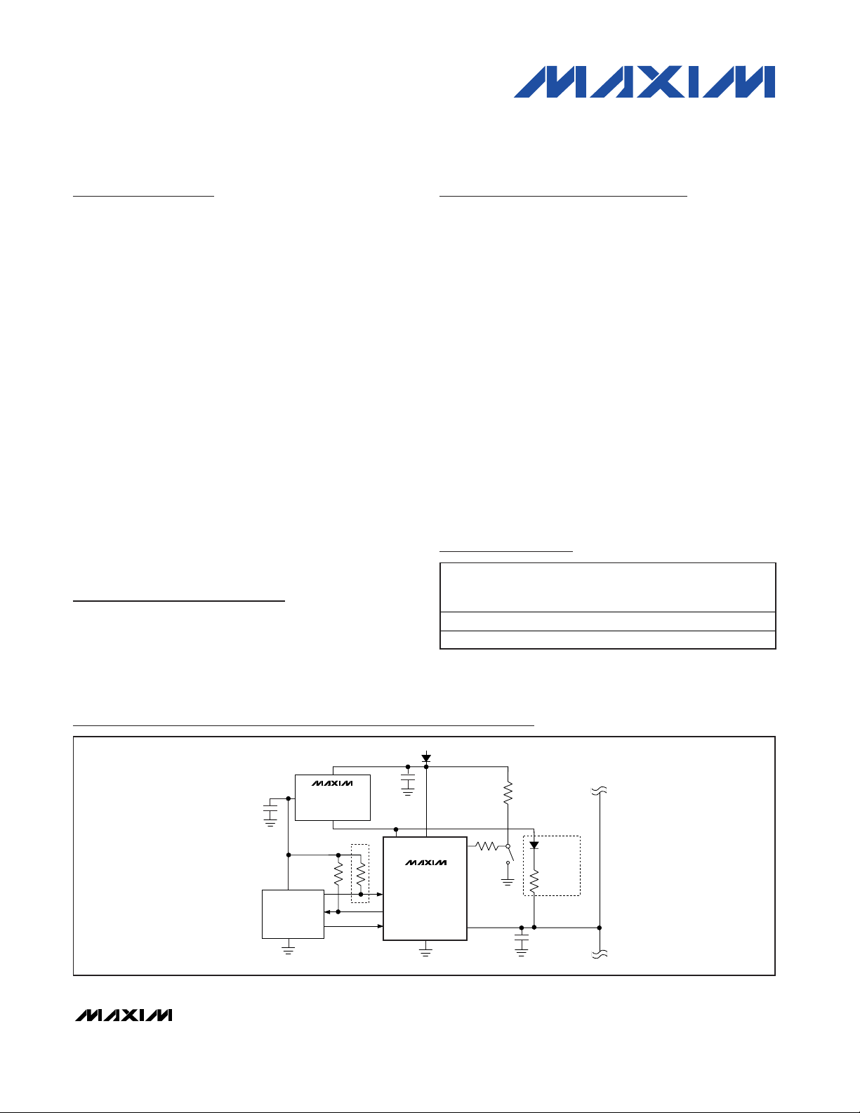
TXD
RXD
NSLP
LIN
GND
INH
NWAKE
MICROCONTROLLER
LIN
BUS
1kΩ
V
BAT
MASTER NODE
ONLY
+5V LDO
*
EN
MAX5023
MAX13020
MAX13021
*OPTIONAL TXD PULLUP RESISTOR FOR READING WAKE-UP SOURCE FLAG
Typical Operating Circuit
Note: All devices are specified over the -40°C to +125°C automotive temperature range.
+Denotes lead-free package.
Pin Configuration appears at end of data sheet.
M A N A G EM EN T
PACKAGE
Page 2
MAX13020/MAX13021
±60V Fault-Protected LIN Transceivers
2 _______________________________________________________________________________________
ABSOLUTE MAXIMUM RATINGS
Stresses beyond those listed under “Absolute Maximum Ratings” may cause permanent damage to the device. These are stress ratings only, and functional
operation of the device at these or any other conditions beyond those indicated in the operational sections of the specifications is not implied. Exposure to
absolute maximum rating conditions for extended periods may affect device reliability.
(All voltages referenced to GND, unless otherwise noted.
Positive currents flow into the device.)
BAT.........................................................................-0.3V to +40V
TXD, RXD, NSLP.......................................................-0.3V to +7V
LIN ...........................................................0V to ±60V Continuous
LIN to BAT..........................................................-80V Continuous
NWAKE...................................................................-0.3V to +80V
NWAKE Current (NWAKE < -0.3V) ....................................-15mA
INH ..............................................................-0.3V to V
BAT
+ 0.3V
INH Current .......................................................-50mA to +15mA
Continuous Power Dissipation
8-Pin SO (derate 5.9mW/°C above +70°C)...................471mW
Operating Temperature Range .........................-40°C to +125°C
Storage Temperature Range .............................-65°C to +150°C
Junction Temperature......................................................+150°C
Lead Temperature (soldering, 10s) ................................+300°C
ELECTRICAL CHARACTERISTICS
(V
BAT
= +5V to +38V, TA= -40°C to +125°C, unless otherwise noted. Typical values are at V
BAT
= +12V and TA= +25°C. Positive
currents flow into the device.)
PARAMETER
SYMBOL
CONDITIONS
MIN
TYP
MAX
UNITS
BAT Supply Voltage V
BAT
Operating range 5.0
V
V
BAT
= +27V,
V
LIN
= V
BAT
148
Sleep mode,
V
NWAKE
= V
BAT,
V
BAT
= +38V,
V
LIN
= V
BAT
8
Standby mode, bus recessive,
V
BAT
= +5V to +27V,
V
LIN
= V
INH
= V
NWAKE
= V
BAT,
V
TXD
= V
NSLP
= GND
Standby mode, bus dominant,
V
BAT
= +12V, V
INH
= V
NWAKE
= V
BAT,
V
LIN
= V
TXD
= V
NSLP
= GND
Normal/low slope mode,
bus recessive, V
BAT
= +5V to +27V,
V
LIN
= V
INH
= V
NWAKE
= V
BAT,
V
TXD
= V
NSLP
= +5V
µA
Normal/low slope mode,
bus dominant, no load,
V
BAT
= V
INH
= V
NWAKE
= +12V,
V
TXD
= GND, V
NSLP
= +5V
1 4.5 8 mA
Sleep mode, bus dominant,
V
BAT
= V
NWAKE
= +12V,
V
LIN
= V
TXD
= V
NSLP
= GND
90
Fault mode, bus dominant (MAX13021),
V
INH
= V
NWAKE
= V
BAT
,
V
LIN
= GND, V
NSLP
= +5V
30 60
BAT Supply Current I
BAT
Disable mode, bus dominant (MAX13021),
20 30
µA
38.0
V
TXD
= V
NSLP
= GND
V
= V
BA T
IN H
= V
N WAK E
= + 12V , V
= G N D
LI N
100 650 1000
300 1000 2000
100 650 1000
Page 3
MAX13020/MAX13021
±60V Fault-Protected LIN Transceivers
_______________________________________________________________________________________ 3
ELECTRICAL CHARACTERISTICS (continued)
(V
BAT
= +5V to +38V, TA= -40°C to +125°C, unless otherwise noted. Typical values are at V
BAT
= +12V and TA= +25°C. Positive
currents flow into the device.)
PARAMETER SYMBOL CONDITIONS
UNITS
TRANSMITTER DATA INPUT (TXD)
High-Level Input Voltage V
IH
Output recessive 2 V
Low-Level Input Voltage V
IL
Output dominant 0.8 V
Pulldown Resistance R
TXD
kΩ
Low-Level Input Current I
IL
V
TXD
= GND -5 0 +5 µA
Low-Level Output Current I
OL
Standby mode, V
NWAKE
= GND,
V
LIN
= V
BAT
, V
TXD
= +0.4V,
local wake-up request
1.5 6 mA
RECEIVER DATA OUTPUT (RXD)
Low-Level Output Current I
OL
V
LIN
= GND, V
RXD
= +0.4V 1.2 4.1 mA
High-Level Leakage Current I
LH
Normal/low slope mode,
V
LIN
= V
BAT
, V
RXD
= +5V
-5 0 +5 µA
NSLP INPUT
High-Level Input Voltage V
IH
2V
Low-Level Input Voltage V
IL
0.8 V
Pulldown Resistance R
NSLP
V
NSLP
= +5V
kΩ
Low-Level Input Current I
IL
V
NSLP
= GND -5 0 +5 µA
NWAKE INPUT
High-Level Input Voltage V
IH
V
BAT
- 1.0 V
Low-Level Input Voltage V
IL
V
NWAKE Pullup Current I
IL
V
NWAKE
= GND -30
-3 µA
High-Level Leakage Current I
LH
V
NWAKE
= +38V, V
BAT
= +38V -5 0 +5 µA
INH OUTPUT
Switch On-Resistance Between
BAT and INH
R
SW
S tand b y, nor m al /l ow sl op e m od es, I
IN H
=
- 15m A, V
BAT
= + 12V
22 50 Ω
High-Level Leakage Current I
LH
Sleep mode,
V
NWAKE
= +38V, V
BAT
= +38V
-5 0 +5 µA
LIN BUS I/O
LIN Recessive Output Voltage
)
V
TXD
= +5V, I
LIN
= -1µA V
BAT
-1.0V V
LIN Dominant Output Voltage V
O(DOM)
Normal/low slope mode,
V
TXD
= GND, V
BAT
= +7V to +27V,
R
TERM
= 500Ω to BAT
V
MIN TYP MAX
125 330 800
125 330 800
-10
V
V
O(RECES
0.2 x V
BAT
- 3.3
BAT
Page 4

MAX13020/MAX13021
±60V Fault-Protected LIN Transceivers
4 _______________________________________________________________________________________
ELECTRICAL CHARACTERISTICS (continued)
(V
BAT
= +5V to +38V, TA= -40°C to +125°C, unless otherwise noted. Typical values are at V
BAT
= +12V and TA= +25°C. Positive
currents flow into the device.)
PARAMETER SYMBOL CONDITIONS
MIN
TYP
MAX
UNITS
High-Level Leakage Current I
LH
V
LIN
= V
BAT
, V
TXD
= +5V -5 0 +5 µA
Device Leakage Current, V
BAT
Disconnected
I
L(BAT)
V
BAT
= GND, V
LIN
= +18V -5 0 +5 µA
Device Leakage Current, GND
Disconnected
I
L(GND)
V
BAT
= GND, V
LIN
= -18V
0µA
LIN Current After Short Detection
I
IL(FAULT)
Fault mode, disable mode (MAX13021)
V
LIN
= GND
-10 -2 µA
Short-Circuit Recovery Threshold
Voltage
)
Fault mode, disable mode (MAX13021)
V
BAT
-
2.5
V
BAT
-
0.9
V
LIN Pullup Current I
IL
-10 -2 µA
Slave Termination Resistance to
V
BAT
R
SLAVE
S tand b y, nor m al /l ow sl op e m od es, V
LIN
=
GN D , V
BAT
= + 12V
20 30 47 kΩ
V
LIN
= V
BAT
= +12V,
V
TXD
= GND, t < t
DOM
27 40 60
V
LIN
= +12V, V
BAT
= +27V,
V
TXD
= GND, t < t
DOM
(Note 1)
45 70 100
Short-Circuit Output Current I
O(SC)
t < t
DOM
45
mA
Receiver Dominant State V
th(DOM)
V
BAT
= +7V to +38V
V
Receiver Recessive State V
th(REC)
V
BAT
= +7V to +38V 0.6 x V
BAT
V
Receiver-Threshold Center
Voltage
)
V
BAT
= +7V to +38V
0.475 x
0.5 x
0.525 x
V
Receiver-Threshold Hysteresis
Voltage
V
th(HYS)
V
BAT
= +7V to +38V
0.145 x
0.16 x
0.175 x
V
Thermal-Shutdown Threshold T
SHDN
°C
Thermal-Shutdown Hysteresis 10 °C
ESD PROTECTION
Human Body Model LIN
kV
Contact Discharge
IEC61000-4-2
LIN, NWAKE, BAT
(tested to IBEE test setup)
C
1
= 100nF on V
BAT
,
C
2
= 220pF on LIN,
R = 33kΩ on NWAKE
±4 kV
V
th(RECOVERY
-100
Sleep mode, V
= GND, V
LIN
NSLP
= GND
V
= +12V, V
BAT
= +60V, V
LIN
V
th(CENTER
= GND,
TXD
V
V
BAT
BAT
V
V
+165
±12
0.4 x V
BAT
BAT
BAT
V
BAT
V
BAT
Page 5

MAX13020/MAX13021
±60V Fault-Protected LIN Transceivers
_______________________________________________________________________________________ 5
TIMING CHARACTERISTICS
(V
BAT
= +5V to +38V, TA= -40°C to +125°C, unless otherwise noted. Typical values are at V
BAT
= +12V and TA= +25°C. Positive
currents flow into the device.)
PARAMETER SYMBOL CONDITIONS
UNITS
LIN Duty Factor 1
D1 = t
BUS(REC)(MAX)
/(2 x t
BIT
)
D1
V
BAT
= +7V to +18V, V
th(REC)(MAX)
=
0.744 x V
BAT,
V
th(DOM)(MAX)
= 0.581 x V
BAT,
t
BIT
= 50µs (Figure 4, Note 2)
—
LIN Duty Factor 2
D2 = t
BUS(REC)(MAX)
/(2 x t
BIT
)
D2
V
BAT
= +8V to +18V,
V
th(REC)(MIN)
= 0.422 x V
BAT,
V
th(DOM)(MIN)
= 0.284 x V
BAT,
t
BIT
= 50µs (Figure 4, Note 2)
—
LIN Duty Factor 3
D3 = t
BUS(REC)(MAX)
/(2 x t
BIT
)
D3
V
BAT
= +7V to +18V,
V
th(REC)(MAX)
= 0.778 x V
BAT,
V
th(DOM)(MAX)
= 0.616 x V
BAT,
t
BIT
= 96µs (Figure 4, Note 2)
—
LIN Duty Factor 4
D4 = t
BUS(REC)(MAX)
/(2 x t
BIT
)
D4
V
th(REC)(MIN)
= 0.389 x V
BAT,
V
th(DOM)(MIN)
= 0.251 x V
BAT
,
V
BAT
= +8V to +18V,
t
BIT
= 96µs (Figure 4, Note 2)
—
Propagation Delay of Receiving
Node
t
p(RX)
V
BAT
= +7V to +18V,
C
RXD
= 20pF (Figure 4)
6µs
Receiver Propagation Delay
Symmetry
t
p(RX)(SYM)
V
BAT
= +7V to +18V,
C
RXD
= 20pF, R
RXD
= 1kΩ
-2 +2 µs
Continuously Dominant-Clamped
LIN Bus Detection Time
)
Normal/low slope mode (MAX13021),
V
LIN
= GND
40 80
ms
Continuously Dominant-Clamped
LIN Bus Recovery Time
)
Normal/low slope mode (MAX13021),
V
LIN
= GND
0.5 1 2 ms
Dominant Time for Wake-Up of
the LIN Transceiver
t
BUS
Sleep mode (Figure 3) 30 70
µs
TXD Permanent Dominant
Disable Time
)
Normal/low slope mode,
V
TXD
= GND
20 80 ms
Dominant Time for Wake-Up
Through NWAKE
t
NWAKE
Sleep mode 7 20 50 µs
Rising edge with respect to falling edge,
t
LIN(DOM)(DET
t
LIN(DOM)(REC
t
TXD(DOM)(DIS
MIN TYP MAX
0.396
0.581
0.417
0.590
160
150
Page 6

MAX13020/MAX13021
±60V Fault-Protected LIN Transceivers
6 _______________________________________________________________________________________
TIMING CHARACTERISTICS (continued)
(V
BAT
= +5V to +38V, TA= -40°C to +125°C, unless otherwise noted. Typical values are at V
BAT
= +12V and TA= +25°C. Positive
currents flow into the device.)
PARAMETER SYMBOL CONDITIONS
MIN
TYP
MAX
UNITS
Mode Change Time from
Sleep/Standby Mode to
Normal/Low Slope Mode
(Note 3) 2 5 10 µs
Mode Change Time from
Normal/Low Slope Mode to Sleep
Mode
(Note 4) 2 5 10 µs
Note 1: Guaranteed by design for V
BAT
= V
LIN
= +27V.
Note 2: Selected bit time, t
BIT
= 50µs or 96µs (20kbaud or 10.4kbaud). Bus load conditions (C
BUS
/ R
BUS
): 1nF/1kΩ, 6.8nF/660Ω,
10nF/500Ω.
Note 3: t
GOTONORM
is measured from rising edge of N
SLP
to RXD active.
Note 4: t
GOTOSLEEP
is measured from falling edge of N
SLP
to RXD high impedance.
0
2
1
5
4
3
6
7
9
8
10
-40 -10 5-25 203550658095110125
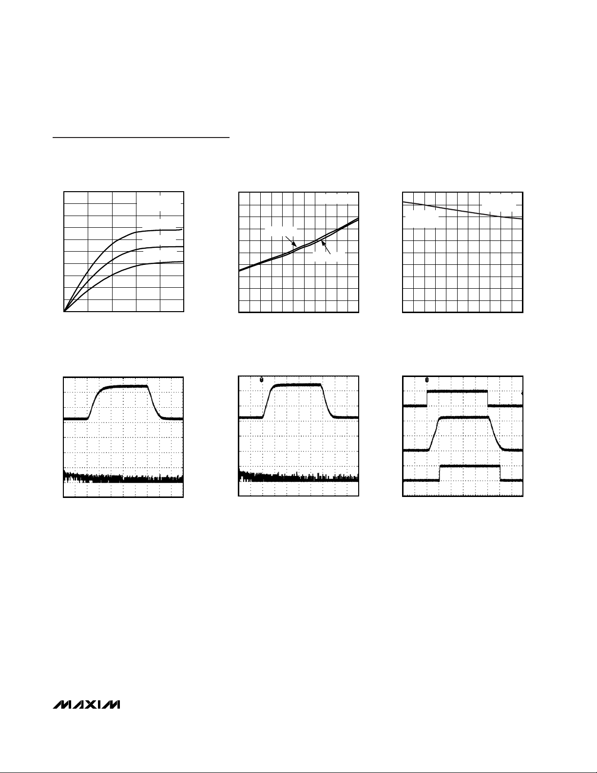
SUPPLY CURRENT
vs. TEMPERATURE
MAX13020 toc01
TEMPERATURE (°C)
SUPPLY CURRENT (mA)
SLEEP MODE
V
LIN
= V
BAT
V
BAT
= +38V
V
BAT
= +12V
0
5
25
40
50
OPERATING CURRENT
vs. SUPPLY VOLTAGE
MAX13020 toc02
SUPPLY VOLTAGE (V)
OPERATING CURRENT (mA)
5202510 15 30 35 40
LOW SLOPE MODE
10.4kbps
NORMAL SLOPE MODE
20kbps
RL = 500Ω
C
L
= 10nF
RL = 1000Ω
C
L
= 1nF
45
10
35
30
20
15
0
10
5
20
15
25
30
021345
SINK CURRENT vs. RXD OUTPUT
LOW VOLTAGE
MAX13020 toc03
RXD OUTPUT LOW VOLTAGE (V)
SINK CURRENT (mA)
TA = +125°C
TA = +25°C
TA = -40°C
Typical Operating Characteristics
(V
BAT
= +12V and TA= +25°C, unless otherwise noted.)
t
GOTONORM
t
GOTOSLEEP
Page 7
MAX13020/MAX13021
±60V Fault-Protected LIN Transceivers
_______________________________________________________________________________________ 7
0
15
10
5
20
25
30
35
40
45
50
021345
SINK CURRENT vs. TXD PULLDOWN
OUTPUT VOLTAGE
MAX13020 toc04
OUTPUT LOW VOLTAGE (V)
SINK CURRENT (mA)
TA = +125°C
TA = +25°C
TA = -40°C
STANDBY MODE
AFTER A LOCAL
0
10
5
25
20
15
30
35
45
40
50
-40 -10 5-25 203550658095110125
INH ON-RESISTANCE
vs. TEMPERATURE
MAX13020 toc05
TEMPERATURE (°C)
INH ON-RESISTANCE (Ω)
I
SINK
= 15mA
V
BAT
= +38V
V
BAT
= +12V
0
20
10
50
40
30
60
70
90
80
100
-40 -10 5-25 20 35 50 65 80 95 110 125
I
BAT
FAULT CURRENT
vs. TEMPERATURE
MAX13020 toc06
TEMPERATURE (°C)
I
BAT
FAULT CURRENT (µA)
MAX13020
V
BAT
= +12V
SLEEP MODE
V
LIN
= 0V
10µs/div
2.5MHz/div
LIN OUTPUT SPECTRUM
LIN
5V/div
FFT
20dB/div
MAX13020 toc07
RL = 660Ω
C
L
= 6.8nF
NORMAL SCOPE MODE
20kbps
20µs/div
2.5MHz/div
LIN OUTPUT SPECTRUM
LIN
5V/div
FFT
20dB/div
MAX13020 toc08
RL = 660Ω
C
L
= 6.8nF
LOW SCOPE MODE
10.4kbps
20µs/div
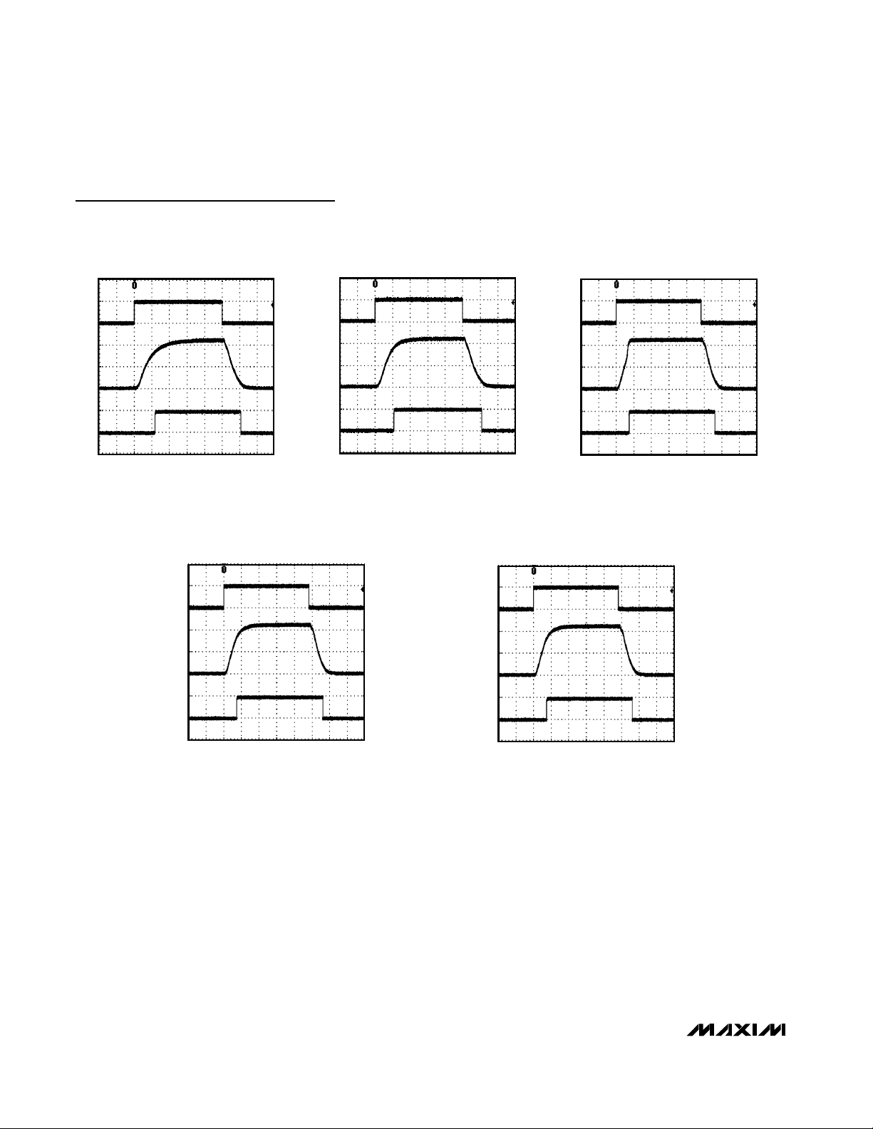
LIN TRANSMITTING NORMAL
SLOPE MODE
TX
5V/div
RX
5V/div
MAX13020 toc09
RL = 1kΩ
C
L
= 1nF
NORMAL SCOPE MODE
20kbps
LIN
5V/div
Typical Operating Characteristics (continued)
(V
BAT
= +12V and TA= +25°C, unless otherwise noted.)
Page 8
MAX13020/MAX13021
±60V Fault-Protected LIN Transceivers
8 _______________________________________________________________________________________
Typical Operating Characteristics (continued)
(V
BAT
= +12V and TA= +25°C, unless otherwise noted.)
10µs/div
LIN TRANSMITTING NORMAL
SLOPE MODE
TX
5V/div
RX
5V/div
MAX13020 toc10
RL = 660kΩ
C
L
= 6.8nF
NORMAL SCOPE MODE
20kbps
LIN
5V/div
10µs/div
TX
5V/div
RX
5V/div
MAX13020 toc11
RL = 500kΩ
C
L
= 10nF
NORMAL SCOPE MODE
20kbps
LIN
5V/div
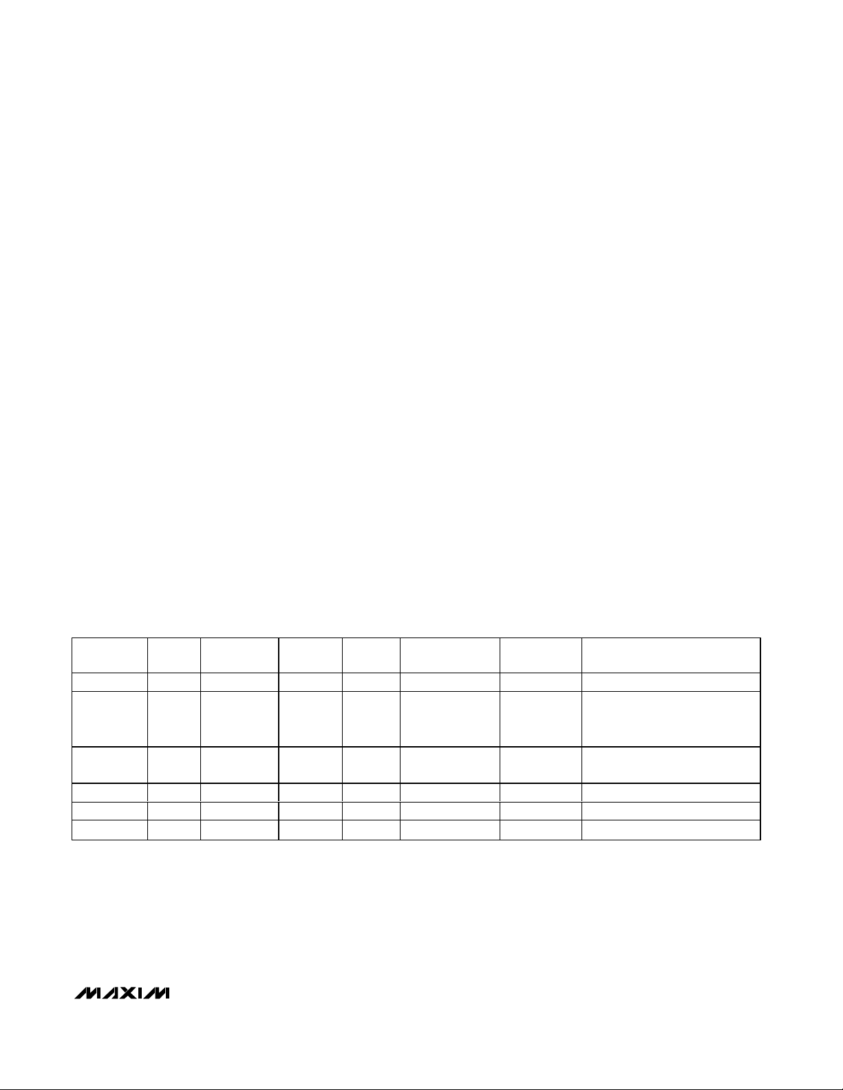
LIN TRANSMITTING NORMAL
SLOPE MODE
20µs/div
TX
5V/div
RX
5V/div
MAX13020 toc12
RL = 1kΩ
C
L
= 1nF
LOW SCOPE MODE
10.4kbps
LIN
5V/div
LIN TRANSMITTING LOW
SLOPE MODE
20µs/div
TX
5V/div
RX
5V/div
MAX13020 toc13
RL = 660kΩ
C
L
= 6.8nF
LOW SCOPE MODE
10.4kbps
LIN
5V/div
LIN TRANSMITTING LOW
SLOPE MODE
20µs/div
TX
5V/div
RX
5V/div
MAX13020 toc14
RL = 500kΩ
C
L
= 10nF
LOW SCOPE MODE
10.4kbps
LIN
5V/div
LIN TRANSMITTING LOW
SLOPE MODE
Page 9

Detailed Description
The MAX13020/MAX13021 ±60V fault-protected lowpower local interconnect network (LIN) transceivers are
ideal for use in automotive network applications where
high reliability is required. The devices provide the
interface between the LIN master/slave protocol controller and the physical bus described in the LIN 2.0
specification package and SAE J2602 specification.
The devices are intended for in-vehicle subnetworks
with a single master and multiple slaves.
The extended fault-protected voltage range of ±60V on
the LIN bus line allows for use in +12V, +24V, and
+42V automotive applications. The devices allow communication up to 20kbaud, and include slew-rate limited transmitters for enhanced electromagnetic
emissions (EME) performance. The devices feature a
low-power 4µA sleep mode and provide wake-up
source detection.
The MAX13020 is a pin-to-pin replacement and is functionally compatible with the Philips TJA1020. The
MAX13021 includes enhanced bus dominant clamping
fault-management for reduced quiescent current during
LIN bus shorts to GND.
Operating Modes
The MAX13020/MAX13021 provide two different transmitting modes, an intermediate standby mode and a
low-power sleep mode. Normal slope mode allows fullspeed communication at 20kbaud with a slew-limited
transmitter to reduce EME. Low slope mode permits
communication up to 10.4kbaud, and provides addi-
tional slew-rate limiting to further reduce EME. The
transmitting operating mode is selected by the logic
state of NSLP and TXD (Table 1). To enter normal slope
mode or low slope mode, drive TXD logic-high or logiclow, then drive NSLP logic-high for longer than
t
GOTONORM
. The MAX13021 features two additional
operating modes to reduce current consumption during
LIN bus shorts to GND.
On initial power-up, the device enters sleep mode.
MAX13020/MAX13021
±60V Fault-Protected LIN Transceivers
_______________________________________________________________________________________ 9
Pin Description
PIN NAME FUNCTION
1 RXD
Data Receive Output, Open Drain. RXD is logic-low when the LIN bus is dominant. RXD is active low after
a wake-up event from sleep mode.
2 NSLP S l eep Inp ut. D r i ve N S LP l og i c- hi g h or l og i c- l ow to contr ol the op er ati ng m od e. ( S ee Tab l e 1 and Fi g ur es 1, 2)
3
Local Wake-Up Input. Present a falling edge on NWAKE to generate a local wake-up event. Connect
NWAKE to BAT with a 5kΩ resistor if local wake-up is not required.
4 TXD
Data Transmit Input, CMOS Compatible. Drive TXD logic-low to force the LIN bus to a dominant state in
normal/low slope mode.
5 GND Ground
6 LIN
LIN Bus I/O. LIN is terminated with an internal 30kΩ resistor in normal slope, low slope, and standby
modes.
7 BAT
Battery Voltage Input. Bypass BAT to ground with a 0.1µF ceramic capacitor as close to the device as
possible.
8 INH Inhibit Output. INH is active high in standby and normal/low slope modes. (See Table 1)
Figure 1. MAX13020 Operating Modes
NWAKE
t
(t
= 0 AFTER 1 TO 0) > t
NWAKE
t
(LIN = 0 AFTER 1 TO 0)
t
(NSLP = 0 AFTER 1 TO 0)
(NSLP = 1 AFTER 0 TO 1)
> t
GOTONORM
TXD = 1
OR
>t
BUS
> t
GOTOSLEEP
t
(NSLP = 1 AFTER 0 TO 1)
> t
GOTONORM
TXD = 0
NWAKE
STANDBY MODE
t
(NSLP = 1 AFTER 0 TO 1)
> t
GOTONORM
TXD = 0
LOW SLOPE MODE
NORMAL SLOPE MODE
t
(NSLP = 1 AFTER 0 TO 1)
> t
GOTONORM
TXD = 1
t
(NSLP = 0 AFTER 1 TO 0)
SLEEP MODE
POWER-ON STATE
> t
GOTOSLEEP
INITIAL
Page 10

MAX13020/MAX13021
Sleep Mode
Sleep mode is the lowest power operating mode and is
the default state after power is applied to BAT. In sleep
mode, the MAX13020/MAX13021 disable the LIN transmitter and receiver to reduce power consumption. RXD
and INH are high impedance. The internal slave termination resistor between LIN and BAT is disabled, and
only a weak pullup from LIN to BAT is enabled. While in
sleep mode, the MAX13020/MAX13021 transition to
standby mode when a local or remote wake-up event is
detected. For applications with a continuously powered
microprocessor, drive NSLP logic-high for longer than
t
GOTONORM
to force the MAX13020/MAX13021 directly
into normal slope mode if TXD is logic-high, and low
slope mode if TXD is logic-low. From normal slope or
low slope mode, drive NSLP logic-low for longer than
t
GOTOSLEEP
to force the MAX13020/MAX13021 into
sleep mode.
Standby Mode
In standby mode, the LIN transmitter and receiver are
disabled, the internal slave termination resistor between
LIN and BAT is enabled, and the INH output is pulled
high. The MAX13020/MAX13021 transition to standby
mode from sleep mode when a wake-up event is
detected. From standby mode, drive TXD logic-high or
logic-low, then drive NSLP logic-high for longer than
t
GOTONORM
to transition to normal slope or low slope
mode. In standby mode, RXD is driven logic-low to
transmit the wake-up interrupt flag to a microcontroller.
The wake-up source flag is presented on TXD as a
strong pulldown in the case of a local wake-up. In the
case of a remote wake-up, TXD is pulled low by the
internal 330kΩ resistor only. The wake-up interrupt and
wake-up source flag are cleared when the
MAX13020/MAX13021 transition to normal slope mode
or low slope mode.
Normal Slope Mode
In normal slope mode, the MAX13020/MAX13021 provide the physical layer interface to a LIN bus through
RXD and TXD. INH is pulled high and the internal slave
termination resistance from LIN to BAT is enabled. Data
presented on TXD is transmitted on the LIN bus with a
controlled slew rate to limit EME. Drive TXD logic-low to
assert a dominant state on LIN. The LIN bus state is
presented on the open-drain output RXD. A dominant
LIN state produces a logic-low on RXD. From standby
or sleep mode, drive TXD logic-high, then drive NSLP
logic-high for longer than t
GOTONORM
to enter normal
slope mode. Drive NSLP logic-low for longer than
t
GOTOSLEEP
to force the device into sleep mode from
normal slope mode.
±60V Fault-Protected LIN Transceivers
10 ______________________________________________________________________________________
NORMAL SLOPE MODE
FAULT MODE
LOW SLOPE MODE
SLEEP MODE
t
(NSLP = 1 AFTER 0 TO 1)
> t
GOTONORM
TXD = 1
t
(LIN = DOMINANT)
> t
LIN(DOM)(DET)
t
(NSLP = 0 AFTER 1 TO 0)
> t
GOTOSLEEP
t
(NSLP = 0 AFTER 1 TO 0)
> t
GOTOSLEEP
t
(NSLP = 1 AFTER 0 TO 1)
> t
GOTONORM
TXD = 0
INITIAL
POWER-ON STATE
STANDBY MODE
t
(NSLP = 1 AFTER 0 TO 1)
> t
GOTONORM
TXD = 1
t
(NSLP = 1 AFTER 0 TO 1)
> t
GOTONORM
TXD = 0
(t
NWAKE
= 0 AFTER 1 TO 0) > t
NWAKE
OR
t
(LIN = 0 AFTER 1 TO 0)
>t
BUS
t
(LIN = RECESSIVE)
> t
LIN(DOM)(REC)
DISABLE MODE
t
(NWAKE = 0 AFTER 1 TO 0)
> t
NWAKE
t
(NSLP = 0 AFTER 1 TO 0)
> t
GOTOSLEEP
t
(NSLP = 1 AFTER 0 TO 1)
> t
GOTONORM
t
(LIN = DOMINANT)
> t
LIN(DOM)(DET)
t
(LIN = RECESSIVE)
> t
LIN(DOM)(REC)
Figure 2. MAX13021 Operating Modes
Page 11
Low Slope Mode
Low slope mode is identical to normal slope mode, with
the exception of the LIN transmitter. In low slope mode,
the transmitter slew-rate is further limited for improved
EME performance. Maximum data rate is limited to
10.4kbaud due to the increased slew-rate limiting of the
LIN transmitter. From standby or sleep mode, drive
TXD logic-low, then drive NSLP logic-high for longer
than t
GOTONORM
to enter low slope mode. Drive NSLP
logic-low for longer than t
GOTOSLEEP
to force the
device into sleep mode from low slope mode.
LIN Bus Dominant Management
(MAX13021)
The MAX13021 provides two additional states to implement reduced current consumption during a LIN-toGND short condition. When the MAX13021 detects a
dominant-clamped fault on LIN, the device disables the
transmitter and enters a low-power fail-safe mode. The
receiver is disabled and a low-power comparator is
enabled to monitor the LIN bus. When a recessive state
is detected on LIN, the device exits fault mode and
returns to standby mode.
Fault Mode (MAX13021)
The device enters fault mode from normal slope or low
slope mode when a dominant state is detected on LIN
for longer than t
LIN(DOM)(DET)
. In fault mode, the slave
termination resistor from LIN to BAT is disconnected,
and the LIN transmitter and receiver are disabled to
reduce power consumption. INH output remains pulled
high. A low-power comparator is enabled to monitor the
LIN bus. Fault mode is cleared, and the MAX13021
enters standby mode when a recessive state is detected on LIN for longer than t
LIN(DOM)(REC)
.
Disable Mode (MAX13021)
The MAX13021 enters disable mode from fault mode
after NSLP is driven logic-low for longer than
t
GOTOSLEEP
. The INH output is high impedance in disable mode to reduce current consumption. The LIN
transmitter and receiver are disabled, and the slave termination resistor from LIN to BAT is disconnected. A
low-power comparator is enabled to monitor the LIN
bus. The MAX13021 enters fault mode when NSLP is
driven logic-high for longer than t
GOTONORM
. The
device enters sleep mode if a recessive state is detected on LIN for longer than t
LIN(DOM)(REC)
.
Local and Remote Wake-Up Events
The MAX13020/MAX13021 recognize local and remote
wake-up events from sleep mode. The MAX13021 also
recognizes local wake-up events from disable mode. A
local wake-up event is detected when NWAKE is held
at logic-low for longer than t
GOTONORM
after a falling
edge. NWAKE is internally pulled up to BAT with a
MAX13020/MAX13021
±60V Fault-Protected LIN Transceivers
______________________________________________________________________________________ 11
MODE
NSLP
TXD
RXD INH
TRANSMITTER
RECEIVER
COMMENTS
SLEEP 0 330kΩ
Disabled Disabled No wake-up events detected
STANDBY 0
330kΩ or
strong
pulldown
0 1 Disabled Disabled
Wake-up detected from sleep
mode. TXD indicates wake-up
source. (Note 1)
NORMAL
SLOPE
1 330kΩ LIN 1 Normal slope Enabled (Notes 2, 3, 4)
LOW SLOPE
1 330kΩ LIN 1 Low slope Enabled (Notes 2, 3, 5)
FAULT* 1 330kΩ LIN 1 Disabled
—
DISABLE* 0 330kΩ LIN
Disabled
—
Table 1. Operating Modes
Note 1: Standby mode is entered automatically after a local or remote wake-up event from sleep mode. INH and the 30kΩ termina-
tion resistor on LIN are enabled.
Note 2: The internal wake-up source flag on TXD is cleared upon entering normal slope or low slope mode.
Note 3: The internal wake-up interrupt flag on RXD is cleared upon entering normal slope or low slope mode.
Note 4: Drive NSLP high for longer than t
GOTONORM
with TXD logic-high to enter normal slope mode.
Note 5: Drive NSLP high for longer than t
GOTONORM
with TXD logic-low to enter low slope mode.
*MAX13021 only.
High-Z = High impedance.
PULLDOWN
High-Z High-Z
High-Z
Low power
Low power
Page 12

MAX13020/MAX13021
10µA pullup. In applications where local wake-up capability is not required, connect NWAKE to BAT. For
improved EMI performance, connect NWAKE to BAT
through a 5kΩ resistance.
A remote wake-up event is generated when a recessive-dominant-recessive sequence is detected on LIN.
The dominant state must be asserted longer than t
BUS
to generate a remote wake-up (Figure 3).
Wake-Up Source Recognition
When a wake-up event is detected, the MAX13020/
MAX13021 enter standby mode and present the wake-up
interrupt on RXD as a logic-low. The wake-up source flag
is presented on TXD as a strong pulldown in the case of a
local wake-up. In the case of a remote wake-up, TXD is
pulled low by the internal 330kΩ resistor only. To read the
wake-up source flag, pull TXD high with an external
pullup resistor (see Reading the Wake-Up Source Flag
section.) The wake-up interrupt and wake-up source flag
are cleared when the MAX13020/MAX13021 transition to
normal slope mode or low slope mode. The thermal-shutdown circuit forces the driver outputs into high-impedance state if the die temperature exceeds +160°C.
Normal operation resumes when the die temperature
cools to +140°C.
Fail-Safe Features
The MAX13020/MAX13021 include a number of failsafe features to handle fault conditions. Internal pulldowns are provided on control inputs TXD and NSLP to
force the device into a known state in the event that
these inputs are disconnected.
LIN Short-Circuit Protection
The LIN transmitter is current-limited to prevent damage from LIN-to-BAT shorts.
TXD Dominant Timeout
If TXD is shorted to GND or is otherwise held low, the
resulting dominant LIN state blocks traffic on the LIN
bus. In normal slope and low slope modes, the LIN
transmitter is disabled if TXD is held at logic-low for
longer than t
TXD(DOM)(DIS)
. The transmitter is re-
enabled on the next rising edge on TXD.
Loss of Power
If BAT or GND are disconnected, interrupting power to
the MAX13020/MAX13021, LIN remains high impedance to avoid loading the LIN bus. Additionally, RXD is
high impedance when BAT is disconnected, preventing
current flow from a connected microcontroller.
LIN Bus Dominant Management (MAX13021)
The MAX13021 provides LIN bus dominant management protection to reduce current consumption during
a LIN-to-GND short condition. When the LIN-to-GND
short is cleared, and a recessive LIN state is detected,
the MAX13021 returns to standby or sleep mode.
ESD Protection
As with all Maxim devices, ESD-protection structures
are incorporated on all pins to protect against ESDs
encountered during handling and assembly. The LIN,
NWAKE, and BAT pins are protected up to ±4kV as
measured by the IEC61000-4-4 Contact Discharge
Model. LIN is protected to ±12kV Human Body Model.
Protection structures prevent damage caused by ESD
events in all operating modes and when the device is
unpowered.
ESD Test Conditions
ESD performance depends on a variety of conditions.
Contact Maxim for a reliability report documenting test
setup, methodology, and results.
Applications Information
Master LIN Nodes
Configure the MAX13020/MAX13021 as a master LIN
node by connecting a 1kΩ resistor from LIN to INH with
a blocking diode (see the Typical Operating Circuit.)
INH is held at a logic-high level in normal slope, low
slope, standby, and fault (MAX13021) modes. INH is
high impedance in sleep mode and disable mode
(MAX13021) to reduce power consumption.
±60V Fault-Protected LIN Transceivers
12 ______________________________________________________________________________________
STANDBY
MODE
V
LIN
LIN RECESSIVE
LIN DOMINANT
t
BUS
0.4 x V
BAT
0.6 x V
BAT
SLEEP MODE
Figure 3. Remote Wake-Up Timing
Page 13

Reading the Wake-Up Source Flag
When a wake-up event is detected in sleep mode, the
MAX13020/MAX13021 transition to standby mode and
present the wake-up source flag on TXD as a strong
pulldown in the case of a local wake-up. In the case of
a remote wake-up event, TXD is pulled to ground only
by an internal resistor. The wake-up source flag can be
determined by connecting a pullup resistor to TXD.
Choose the external pullup resistor such that TXD is a
logic-high when a remote wake-up occurs, and when a
local wake-up occurs and the strong pulldown drives
TXD low.
MAX13020/MAX13021
±60V Fault-Protected LIN Transceivers
______________________________________________________________________________________ 13
t
BIT
t
BIT
t
BIT
t
BUS(DOM)(MAX)
t
BUS(REC)(MIN)
V
TH(REC)(MAX)
V
TH(DOM)(MAX)
V
TH(REC)(MIN)
V
TH(DOM)(MIN)
t
BUS(DOM)(MIN)
t
BUS(REC)(MAX)
t
P(rx1)F
t
P(rx1)F
t
P(rx2)F
t
P(rx2)F
THRESHOLDS OF
RECEIVING NODE 1
THRESHOLDS OF
RECEIVING NODE 1
V
TXDL
V
SUP
(1)
LIN BUS
SIGNAL
V
RXDL1
V
RXDL2
RECEIVING
NODE 1
RECEIVING
NODE 2
(1) TRANSCEIVER SUPPLY OF TRANSMITTING NODE.
Figure 4. LIN Waveform Definition
BAT
NWAKE
TXD
INH
NSLP
GND
LIN
RXD
0.1µF
R
L
C
L
+5V
MAX13020
MAX13021
Figure 5. Test Circuit for AC Characteristics
Page 14

MAX13020/MAX13021
±60V Fault-Protected LIN Transceivers
14 ______________________________________________________________________________________
Chip Information
PROCESS: BiCMOS
NSLP
NWAKE
INH
TXD
RXD
BAT
LIN
TXD
TIME-OUT
TIMER
RXD/INT
SLEEP/NORMAL
TIMER
WAKE-UP
TIMER
MODE CONTROL
BUS TIMER
SLEW
RATE
CONTROL
THERMAL
SHUTDOWN
FILTER
30kΩ
GND
VBAT/2
MAX13020
MAX13021
5µA
Functional Diagram
LIN
GNDTXD
1
2
87INH
BATNSLP
NWAKE
RXD
SO
TOP VIEW
3
4
6
5
MAX13020
MAX13021
+
Pin Configuration
Page 15

MAX13020/MAX13021
±60V Fault-Protected LIN Transceivers
Maxim cannot assume responsibility for use of any circuitry other than circuitry entirely embodied in a Maxim product. No circuit patent licenses are
implied. Maxim reserves the right to change the circuitry and specifications without notice at any time.
Maxim Integrated Products, 120 San Gabriel Drive, Sunnyvale, CA 94086 408-737-7600 ____________________ 15
© 2006 Maxim Integrated Products is a registered trademark of Maxim Integrated Products, Inc.
Boblet
Package Information
(The package drawing(s) in this data sheet may not reflect the most current specifications. For the latest package outline information,
go to www.maxim-ic.com/packages
.)
SOICN .EPS
PACKAGE OUTLINE, .150" SOIC
1
1
21-0041
B
REV.DOCUMENT CONTROL NO.APPROVAL
PROPRIETARY INFORMATION
TITLE:
TOP VIEW
FRONT VIEW
MAX
0.010
0.069
0.019
0.157
0.010
INCHES
0.150
0.007
E
C
DIM
0.014
0.004
B
A1
MIN
0.053A
0.19
3.80 4.00
0.25
MILLIMETERS
0.10
0.35
1.35
MIN
0.49
0.25
MAX
1.75
0.050
0.016L
0.40 1.27
0.3940.386D
D
MINDIM
D
INCHES
MAX
9.80 10.00
MILLIMETERS
MIN
MAX
16
AC
0.337 0.344 AB8.758.55 14
0.189 0.197 AA5.004.80 8
N MS012
N
SIDE VIEW
H 0.2440.228 5.80 6.20
e 0.050 BSC 1.27 BSC
C
HE
e
B
A1
A
D
0-8
L
1
VARIATIONS:
 Loading...