

General Description
The MAX1300/MAX1301 multirange, low-power, 16-bit,
successive-approximation, analog-to-digital converters
(ADCs) operate from a single +5V supply and achieve
throughput rates up to 115ksps. A separate digital supply allows digital interfacing with 2.7V to 5.25V systems
using the SPI™-/QSPI™-/MICROWIRE™-compatible
serial interface. Partial power-down mode reduces the
supply current to 1.3mA (typ). Full power-down mode
reduces the power-supply current to 1µA (typ).
The MAX1300 provides eight (single-ended) or four
(true differential) analog input channels. The MAX1301
provides four (single-ended) or two (true differential)
analog input channels. Each analog input channel is
independently software programmable for seven single-ended input ranges (0 to +6V, -6V to 0, 0 to +12V,
-12V to 0, ±3V, ±6V, and ±12V), and three differential
input ranges (±6V, ±12V, ±24V).
An on-chip +4.096V reference offers a small convenient
ADC solution. The MAX1300/MAX1301 also accept an
external reference voltage between 3.800V and 4.136V.
The MAX1300 is available in a 24-pin TSSOP package
and the MAX1301 is available in a 20-pin TSSOP package. Each device is specified for operation from -40°C
to +85°C.
Applications
Industrial Control Systems
Data-Acquisition Systems
Avionics
Robotics
Features
♦ Software-Programmable Input Range for Each
Channel
♦ Single-Ended Input Ranges
0 to +6V, -6V to 0, 0 to +12V, -12V to 0, ±3V,
±6V, and ±12V
♦ Differential Input Ranges
±6V, ±12V, and ±24V
♦ Eight Single-Ended or Four Differential Analog
Inputs (MAX1300)
♦ Four Single-Ended or Two Differential Analog
Inputs (MAX1301)
♦ ±16.5V Overvoltage Tolerant Inputs
♦ Internal or External Reference
♦ 115ksps Maximum Sample Rate
♦ Single +5V Power Supply
♦ 20-/24-Pin TSSOP Package
MAX1300/MAX1301
8-/4-Channel, ±12V Multirange Inputs,
Serial 16-Bit ADCs
________________________________________________________________ Maxim Integrated Products 1
Pin Configurations
Ordering Information
24
23
22
21
20
19
18
17
1
2
3
4
5
6
7
8
AGND1
AGND2
AV
DD2
AGND3CH2
CH1
CH0
AV
DD1
TOP VIEW
REF
REFCAP
DV
DD
DV
DDO
CH6
CH5
CH4
CH3
16
15
14
13
9
10
11
12
DGND
DGNDO
DOUT
SCLKSSTRB
DIN
CS
CH7
TSSOP
MAX1300
19-3575; Rev 1; 11/06
For pricing, delivery, and ordering information, please contact Maxim/Dallas Direct! at
1-888-629-4642, or visit Maxim’s website at www.maxim-ic.com.
EVALUATION KIT
AVAILABLE
SPI and QSPI are trademarks of Motorola, Inc.
MICROWIRE is a trademark of National Semiconductor Corp.
Pin Configurations continued at end of data sheet.
*Future product—contact factory for availability.
PART
MAX1300AEUG*
MAX1300BEUG*
MAX1301AEUP*
MAX1301BEUP
TEMP
RANGE
-40°C to
+85°C
-40°C to
+85°C
-40°C to
+85°C
-40°C to
+85°C
PINPACKAGE
C H A N N EL S
CODE
24 TSSOP 8 U24-1
24 TSSOP 8 U24-1
20 TSSOP 4 U20-2
20 TSSOP 4 U20-2
PKG
MAX1300/MAX1301
8-/4-Channel, ±12V Multirange Inputs,
Serial 16-Bit ADCs
2 _______________________________________________________________________________________
ABSOLUTE MAXIMUM RATINGS
ELECTRICAL CHARACTERISTICS
(AV
DD1
= AV
DD2
= DVDD= DV
DDO
= 5V, AGND1 = DGND = DGNDO = AGND2 = AGND3 = 0, f
CLK
= 3.5MHz (50% duty cycle),
external clock mode, V
REF
= 4.096V (external reference operation), REFCAP = AV
DD1
, maximum single-ended bipolar input range
(±12V), C
DOUT
= 50pF, C
SSTRB
= 50pF, TA= -40°C to +85°C, unless otherwise noted. Typical values are at TA= +25°C.)
Stresses beyond those listed under “Absolute Maximum Ratings” may cause permanent damage to the device. These are stress ratings only, and functional
operation of the device at these or any other conditions beyond those indicated in the operational sections of the specifications is not implied. Exposure to
absolute maximum rating conditions for extended periods may affect device reliability.
AV
DD1
to AGND1 ....................................................-0.3V to +6V
AV
DD2
to AGND2 ....................................................-0.3V to +6V
DVDDto DGND ........................................................-0.3V to +6V
DV
DDO
to DGNDO ..................................................-0.3V to +6V
DVDDto DV
DDO
......................................................-0.3V to +6V
DVDD, DV
DDO
to AV
DD1
........................................-0.3V to +6V
AV
DD1
, DVDD, DV
DDO
to AV
DD2
..........................-0.3V to +6V
DGND, DGNDO, AGND3, AGND2 to AGND1 ......-0.3V to +0.3V
CS, SCLK, DIN, DOUT, SSTRB to
DGNDO ............................................-0.3V to (DV
DDO
+ 0.3V)
CH0–CH7 to AGND1 .........................................-16.5V to +16.5V
REF, REFCAP to AGND1.......................-0.3V to (AV
DD1
+ 0.3V)
Continuous Current (any pin) ...........................................±50mA
Continuous Power Dissipation (T
A
= +70°C)
20-Pin TSSOP (derate 11mW/°C above +70°C) ..........879mW
24-Pin TSSOP (derate 12.2mW/°C above +70°C) .......976mW
Operating Temperature Range ...........................-40°C to +85°C
Junction Temperature .....................................................+150°C
Storage Temperature Range .............................-65°C to +150°C
Lead Temperature (soldering, 10s) .................................+300°C
DC ACCURACY (Notes 1, 2)
Resolution 16 Bits
Integral Nonlinearity INL
Differential Nonlinearity DNL No missing codes -1 +2 LSB
Transition Noise External or internal reference 1 LSB
Offset Error
Channel-to-Channel Gain
Matching
Channel-to-Channel Offset Error
Matching
Offset Temperature Coefficient
Gain Error
Gain Temperature Coefficient
Unipolar Endpoint Overlap
DYNAMIC SPECIFICATIONS f
Signal-to-Noise Plus Distortion SINAD
PARAMETER SYMBOL CONDITIONS MIN TYP MAX UNITS
MAX130_A ±1.0 ±2
MAX130_B ±1.0 ±4
Single-ended inputs
Differential inputs
(Note 3)
Unipolar or bipolar 0.025 %FSR
Unipolar or bipolar 1.0 mV
Unipolar 10
Bipolar 5
Unipolar ±0.5
Bipolar ±0.3
Unipolar 1.5
Bipolar 1.0
Negative unipolar full scale to positive
unipolar zero-scale
IN(SINE-WAVE)
= 5kHz, VIN = FSR - 0.05dB, f
Differential inputs, FSR = 48V 91
Single-ended inputs, FSR = 24V 89
Single-ended inputs, FSR = 12V 86
Single-ended inputs, FSR = 6V 80 83
Unipolar 0 ±20
Bipolar -1.0 ±10
Unipolar 0 ±40
Bipolar -2.0 ±20
= 130ksps (Notes 1, 2)
SAMPLE
0 20 LSB
LSB
RMS
mV
ppm/°C
%FSR
ppm/°C
dB
MAX1300/MAX1301
8-/4-Channel, ±12V Multirange Inputs,
Serial 16-Bit ADCs
_______________________________________________________________________________________ 3
ELECTRICAL CHARACTERISTICS (continued)
(AV
DD1
= AV
DD2
= DVDD= DV
DDO
= 5V, AGND1 = DGND = DGNDO = AGND2 = AGND3 = 0, f
CLK
= 3.5MHz (50% duty cycle),
external clock mode, V
REF
= 4.096V (external reference operation), REFCAP = AV
DD1
, maximum single-ended bipolar input range
(±12V), C
DOUT
= 50pF, C
SSTRB
= 50pF, TA= -40°C to +85°C, unless otherwise noted. Typical values are at TA= +25°C.)
Signal-to-Noise Ratio SNR
Total Harmonic Distortion
(Up to the 5th Harmonic)
Spurious-Free Dynamic Range SFDR 92 99 dB
Aperture Delay t
Aperture Jitter t
Channel-to-Channel Isolation 105 dB
CONVERSION RATE
ANALOG INPUTS (CH0–CH3 MAX1301, CH0–CH7 MAX1300, AGND1)
Small-Signal Bandwidth All input ranges, VIN = 100mV
Full-Power Bandwidth All input ranges, VIN = 4V
Input Voltage Range (Table 6) V
Tr ue- D i ffer enti al Anal og C om m on-
M od e V ol tag e Rang e
Common-Mode Rejection Ratio CMRR DIF/SGL = 1, input voltage range = ±3V 75 dB
Input Current I
Input Capacitance C
Input Resistance R
PARAMETER SYMBOL CONDITIONS MIN TYP MAX UNITS
Differential inputs, FSR = 48V 91
Single-ended inputs, FSR = 24V 89
Single-ended inputs, FSR = 12V 86
Single-ended inputs, FSR = 6V 83
THD -97 dB
AD
AJ
SAMPLE
CH_
V
CMDR
CH_
CH_
CH_
Figure 21 15 ns
Figure 21 100 ps
External clock mode, Figure 2 114
External acquisition mode, Figure 3 84Byte-Wide Throughput Rate f
Internal clock mode, Figure 4 106
(Note 2) 700 kHz
P-P
R[2:1] = 001 -3 +3
R[2:1] = 010 -6 0
R[2:1] = 011 0 +6
R[2:1] = 100 -6 +6
R[2:1] = 101 -12 0
R[2:1] = 110 0 +12
R[2:1] = 111 -12 +12
DIF/SGL = 1 (Note 4) -14 +9 V
-12V < V
< +12V -1250 +900 µA
CH_
(Note 2) 2 MHz
P-P
5pF
17 kΩ
dB
ksps
V
MAX1300/MAX1301
8-/4-Channel, ±12V Multirange Inputs,
Serial 16-Bit ADCs
4 _______________________________________________________________________________________
ELECTRICAL CHARACTERISTICS (continued)
(AV
DD1
= AV
DD2
= DVDD= DV
DDO
= 5V, AGND1 = DGND = DGNDO = AGND2 = AGND3 = 0, f
CLK
= 3.5MHz (50% duty cycle),
external clock mode, V
REF
= 4.096V (external reference operation), REFCAP = AV
DD1
, maximum single-ended bipolar input range
(±12V), C
DOUT
= 50pF, C
SSTRB
= 50pF, TA= -40°C to +85°C, unless otherwise noted. Typical values are at TA= +25°C.)
PARAMETER SYMBOL CONDITIONS MIN TYP MAX UNITS
INTERNAL REFERENCE (Bypass REFCAP with 0.1µF to AGND1 and REF with 1.0µF to AGND1)
Reference Output Voltage V
Reference Temperature
Coefficient
Reference Short-Circuit Current I
Reference Load Regulation I
REF
TC
REF
REFSC
REF shorted to AGND1 10
REF shorted to AV
= 0 to 0.5mA 0.1 10 mV
REF
DD
EXTERNAL REFERENCE (REFCAP = AVDD)
Reference Input Voltage Range V
REFCAP Buffer Disable
Threshold
Reference Input Current I
V
REF
RCTH
REF
(Note 5)
V
= +4.096V, external clock mode,
REF
external acquisition mode, internal clock
mode, or partial power-down mode
V
= +4.096V, full power-down mode ±0.1 ±10
REF
External clock mode, external acquisition
Reference Input Resistance R
REF
mode, internal clock mode, or partial
power-down mode
Full power-down mode 40 MΩ
DIGITAL INPUTS (DIN, SCLK, CS)
Input High Voltage V
Input Low Voltage V
Input Hysteresis V
Input Leakage Current I
Input Capacitance C
IH
IL
HYST
IN
IN
VIN = 0 to DV
DDO
DIGITAL OUTPUTS (DOUT, SSTRB)
DV
Output Low Voltage V
Output High Voltage V
DOUT Tri-State Leakage Current I
POWER REQUIREMENTS (AV
and AGND1, AV
DD1
Analog Supply Voltage AV
Digital Supply Voltage DV
OL
OH
DDO
DD1
DD
= 4.75V, I
DDO
DV
= 2.7V, I
DDO
I
SOURCE
CS = DV
= 0.5mA
DDO
and AGND2, DVDD and DGND, DV
DD2
= 10mA 0.4
SINK
= 5mA 0.4
SINK
DDO
4.056 4.096 4.136 V
±30 ppm/°C
-1
3.800 4.136 V
AV
- 0.4
DD1
AV
DD1
- 0.1
90 200
20 45 kΩ
0.7 x
DV
DDO
0.3 x
DV
DDO
0.2 V
-10 +10 µA
10 pF
DV
DDO
- 0.4
-10 +10 µA
and DGNDO)
4.75 5.25 V
4.75 5.25 V
mA
V
µA
V
V
V
V
MAX1300/MAX1301
8-/4-Channel, ±12V Multirange Inputs,
Serial 16-Bit ADCs
_______________________________________________________________________________________ 5
ELECTRICAL CHARACTERISTICS (continued)
(AV
DD1
= AV
DD2
= DVDD= DV
DDO
= 5V, AGND1 = DGND = DGNDO = AGND2 = AGND3 = 0, f
CLK
= 3.5MHz (50% duty cycle),
external clock mode, V
REF
= 4.096V (external reference operation), REFCAP = AV
DD1
, maximum single-ended bipolar input range
(±12V), C
DOUT
= 50pF, C
SSTRB
= 50pF, TA= -40°C to +85°C, unless otherwise noted. Typical values are at TA= +25°C.)
Preamplifier Supply Voltage AV
Digital I/O Supply Voltage DV
AV
Supply Current I
DD1
DVDD Supply Current I
AV
Supply Current I
DD2
DV
Supply Current I
DDO
Total Supply Current
Power-Supply Rejection Ratio PSRR All analog input ranges ±0.5 LSB
TIMING CHARACTERISTICS (Figures 15 and 16)
SCLK Period t
SCLK Low Pulse Width (Note 6) t
DIN to SCLK Setup t
DIN to SCLK Hold t
SCLK Fall to DOUT Valid t
CS Fall to DOUT Enable t
PARAMETER SYMBOL CONDITIONS MIN TYP MAX UNITS
DD2
DDO
AVDD1
DVDD
AVDD2
DVDDO
CP
CH
CL
DS
DH
DO
DV
External clock mode,
external acquisition
mode, or internal
clock mode
External clock mode, external acquisition
mode, or internal clock mode
External clock mode, external acquisition
mode, or internal clock mode
External clock mode, external acquisition
mode, or internal clock mode
Partial power-down mode 1.3 mA
Full power-down mode 1 µA
External clock mode 272 62
External acquisition mode 228 62
Internal clock mode 100 83
External clock mode 109
External acquisition mode 92SCLK High Pulse Width (Note 6) t
Internal clock mode 40
External clock mode 109
External acquisition mode 92
Internal clock mode 40
Internal reference 3 3.5
External reference 2.5 3
4.75 5.25 V
2.70 5.25 V
0.9 2 mA
17.5 25 mA
0.2 1 mA
40 ns
0ns
40 ns
40 ns
mA
µs
ns
ns
MAX1300/MAX1301
8-/4-Channel, ±12V Multirange Inputs,
Serial 16-Bit ADCs
6 _______________________________________________________________________________________
Note 1: Parameter tested at AV
DD1
= AV
DD2
= DVDD= DV
DDO
= 5V.
Note 2: See definitions in the Parameter Definitions section at the end of the data sheet.
Note 3: Guaranteed by correlation with single-ended measurements.
Note 4: Not production tested. Guaranteed by design.
Note 5: To ensure external reference operation, V
REFCAP
must exceed (AV
DD1
- 0.1V). To ensure internal reference operation, V
REFCAP
must be below (AV
DD1
- 0.4V). Bypassing REFCAP with a 0.1µF or larger capacitor to AGND1 sets V
REFCAP
≈ 4.096V. The tran-
sition point between internal reference mode and external reference mode lies between the REFCAP buffer disable threshold
minimum and maximum values (Figures 17 and 18).
Note 6: The SCLK duty cycle can vary between 40% and 60%, as long as the t
CL
and tCHtiming requirements are met.
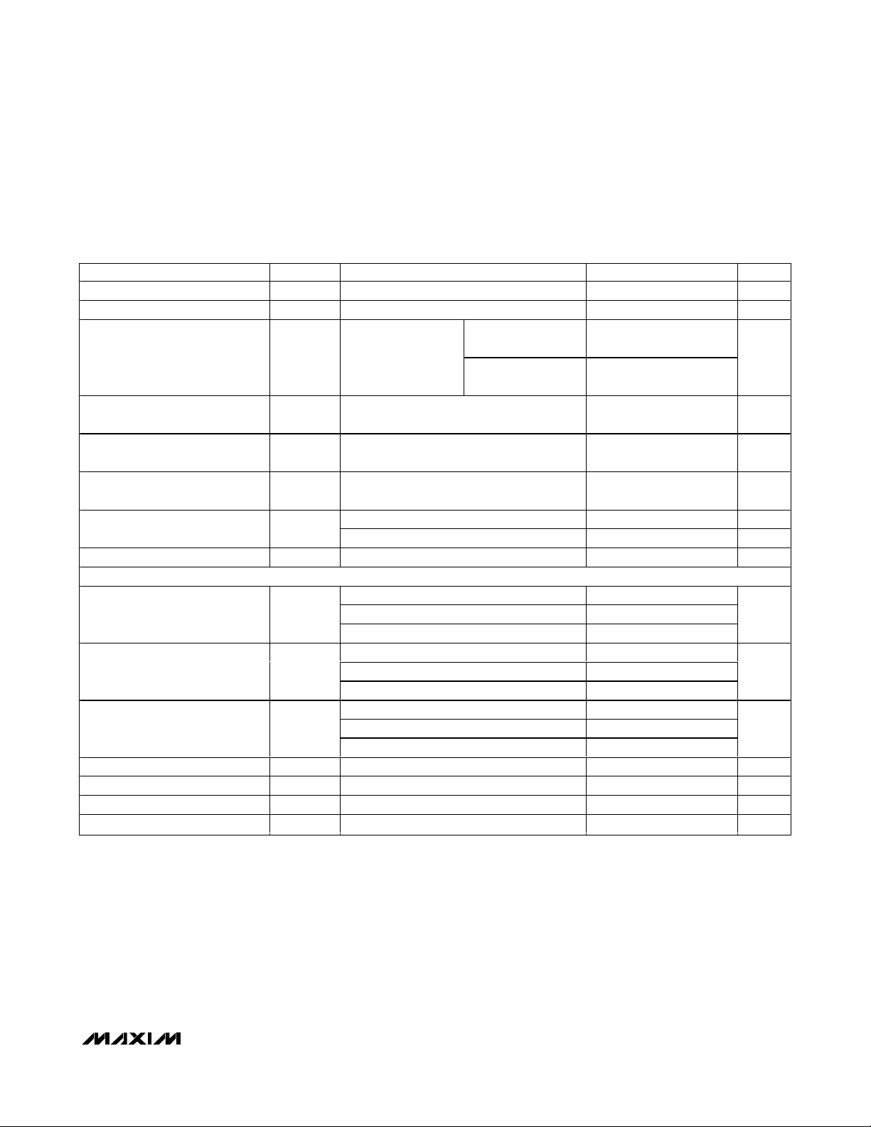
ANALOG SUPPLY CURRENT
vs. ANALOG SUPPLY VOLTAGE
MAX1300/01 toc01
AV
DD1
(V)
I
AVDD1
(mA)
5.155.054.954.85
2.35
2.40
2.45
2.50
2.55
2.60
2.30
4.75 5.25
+85°C
+25°C
-40°C
EXTERNAL CLOCK MODE
PREAMPLIFIER SUPPLY CURRENT
vs. PREAMPLIFIER SUPPLY VOLTAGE
MAX1300/01 toc02
AV
DD2
(V)
I
AVDD2
(mA)
5.155.054.85 4.95
16
17
18
19
20
21
22
23
24
15
4.75 5.25
+85°C
+25°C
-40°C
EXTERNAL CLOCK MODE
DIGITAL SUPPLY CURRENT
vs. DIGITAL SUPPLY VOLTAGE
MAX1300/01 toc03
DVDD (V)
I
DVDD
(mA)
5.155.054.954.85
0.70
0.75
0.80
0.85
0.90
0.65
4.75 5.25
+85°C
+25°C
-40°C
EXTERNAL CLOCK MODE
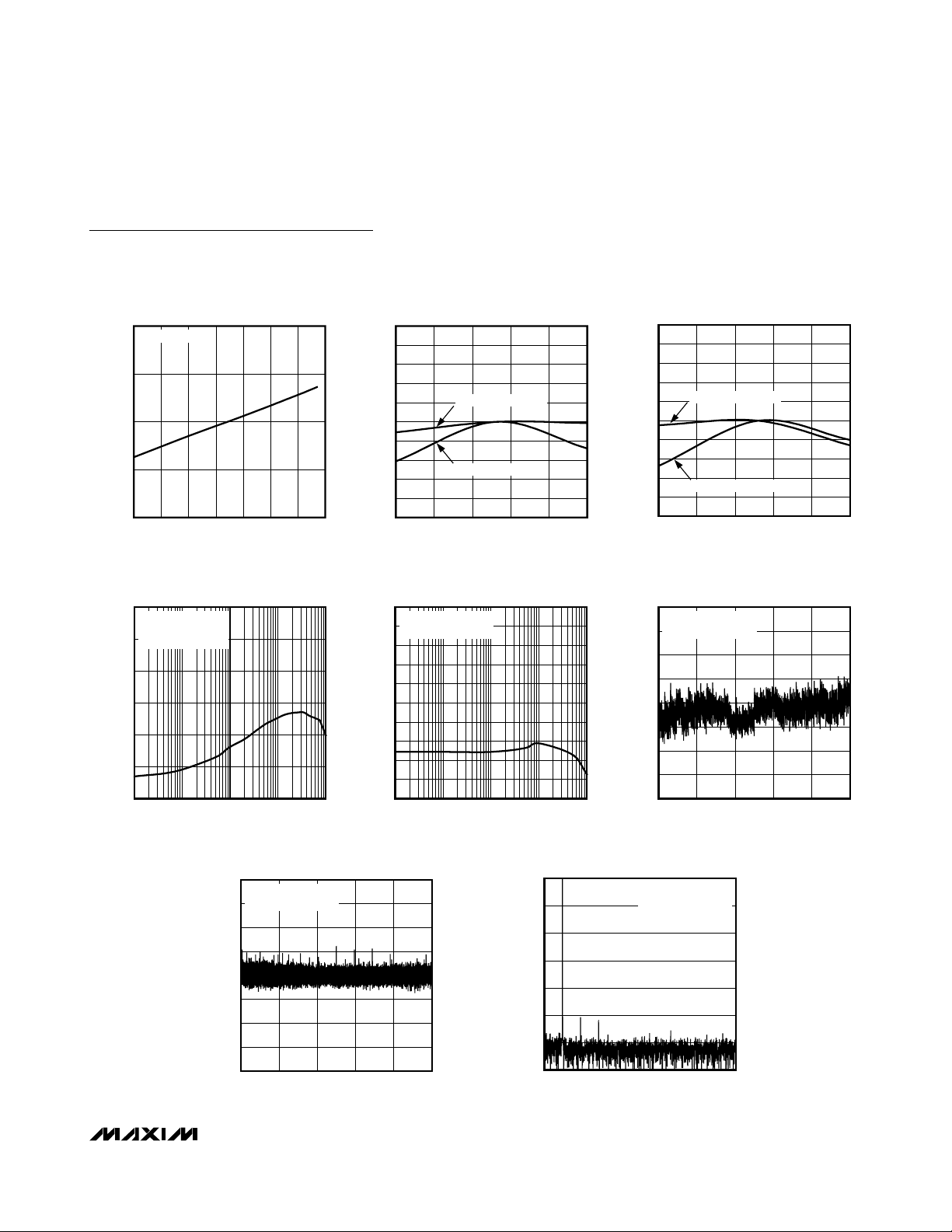
Typical Operating Characteristics
(AV
DD1
= AV
DD2
= DVDD= DV
DDO
= 5V, AGND1 = DGND = DGNDO = AGND2 = AGND3 = 0, f
CLK
= 3.5MHz (50% duty cycle),
external clock mode, V
REF
= 4.096V (external reference operation), REFCAP = AV
DD1
, maximum single-ended bipolar input range,
C
DOUT
= 50pF, C
SSTRB
= 50pF; unless otherwise noted.)
ELECTRICAL CHARACTERISTICS (continued)
(AV
DD1
= AV
DD2
= DVDD= DV
DDO
= 5V, AGND1 = DGND = DGNDO = AGND2 = AGND3 = 0, f
CLK
= 3.5MHz (50% duty cycle),
external clock mode, V
REF
= 4.096V (external reference operation), REFCAP = AV
DD1
, maximum single-ended bipolar input range
(±12V), C
DOUT
= 50pF, C
SSTRB
= 50pF, TA= -40°C to +85°C, unless otherwise noted. Typical values are at TA= +25°C.)
PARAMETER SYMBOL CONDITIONS MIN TYP MAX UNITS
CS Rise to DOUT Disable t
CS Fall to SCLK Rise Setup t
CS High Minimum Pulse Width t
SCLK Fall to CS Rise Hold t
TR
CSS
CSPW
CSH
40 ns
40 ns
0ns
40 ns
SSTRB Rise to CS Fall Setup (Note 4) 40 ns
DOUT Rise/Fall Time CL = 50pF 10 ns
SSTRB Rise/Fall Time CL = 50pF 10 ns
MAX1300/MAX1301
8-/4-Channel, ±12V Multirange Inputs,
Serial 16-Bit ADCs
_______________________________________________________________________________________ 7
I
(
A)
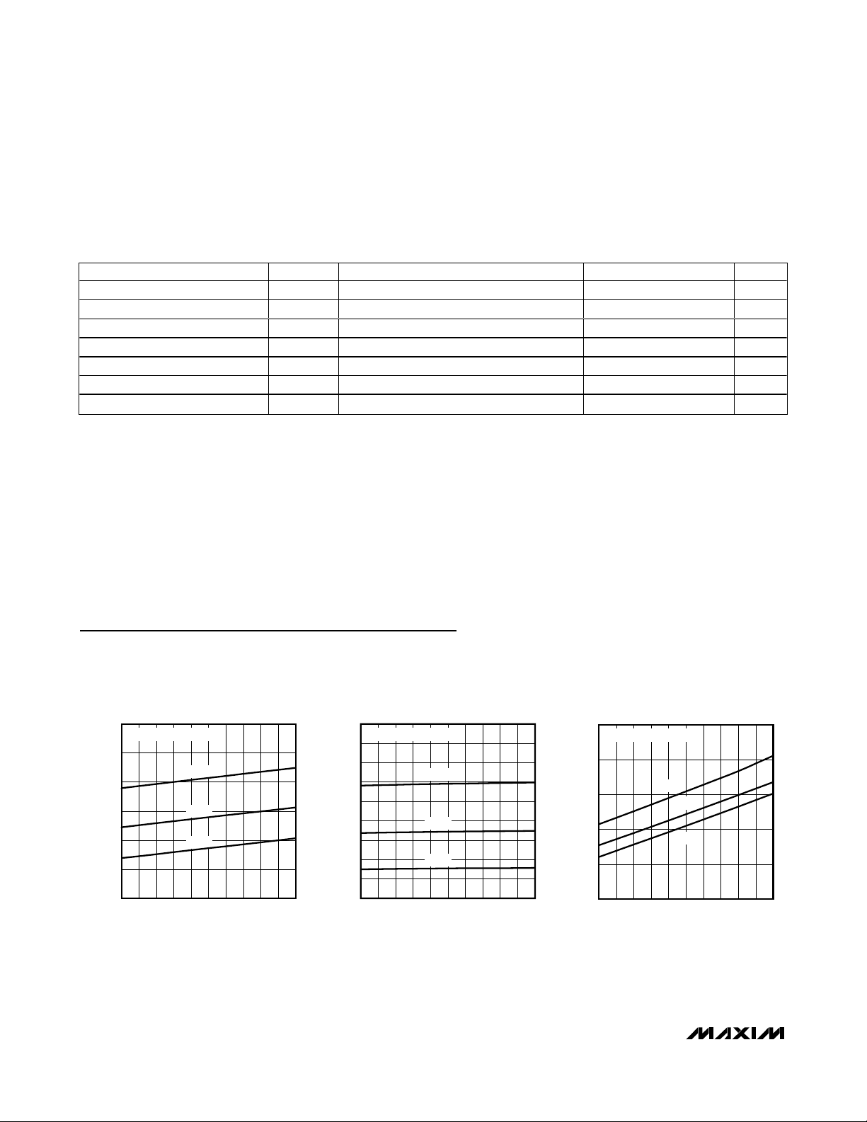
Typical Operating Characteristics (continued)
(AV
DD1
= AV
DD2
= DVDD= DV
DDO
= 5V, AGND1 = DGND = DGNDO = AGND2 = AGND3 = 0, f
CLK
= 3.5MHz (50% duty cycle),
external clock mode, V
REF
= 4.096V (external reference operation), REFCAP = AV
DD1
, maximum single-ended bipolar input range,
C
DOUT
= 50pF, C
SSTRB
= 50pF; unless otherwise noted.)
0.28
0.26
0.24
0.22
0.20
(mA)
0.18
DVDDO
I
0.16
0.14
0.12
0.10
0.20
0.18
0.16
(mA)
AVDD2
I
0.14
0.12
0.10
DIGITAL I/O SUPPLY CURRENT
vs. DIGITAL I/O SUPPLY VOLTAGE
EXTERNAL CLOCK MODE
MAX1300/01 toc04
+85°C
+25°C
-40°C
4.75 5.25
DV
DDO
PREAMPLIFIER SUPPLY CURRENT
vs. PREAMPLIFIER SUPPLY VOLTAGE
PARTIAL POWER-DOWN MODE
+25°C
-40°C
4.75 5.25
AV
DD2
5.155.054.85 4.95
(V)
+85°C
MAX1300/01 toc06
5.155.054.954.85
(V)
ANALOG SUPPLY CURRENT
vs. ANALOG SUPPLY VOLTAGE
0.55
PARTIAL POWER-DOWN MODE
0.53
+85°C
0.51
(mA)
AVDD1
I
0.49
0.47
0.45
4.75 5.25
+25°C
-40°C
AV
(V)
DD1
DIGITAL SUPPLY CURRENT
vs. DIGITAL SUPPLY VOLTAGE
0.136
PARTIAL POWER-DOWN MODE
0.134
0.132
0.130
m
0.128
DVDD
0.126
0.124
0.122
0.120
4.75 5.25
+85°C
-40°C
+25°C
DVDD (V)
MAX1300/01 toc05
5.155.054.954.85
MAX1300/01 toc07
5.154.85 5.054.95
MAX1300/MAX1301
8-/4-Channel, ±12V Multirange Inputs,
Serial 16-Bit ADCs
8 _______________________________________________________________________________________
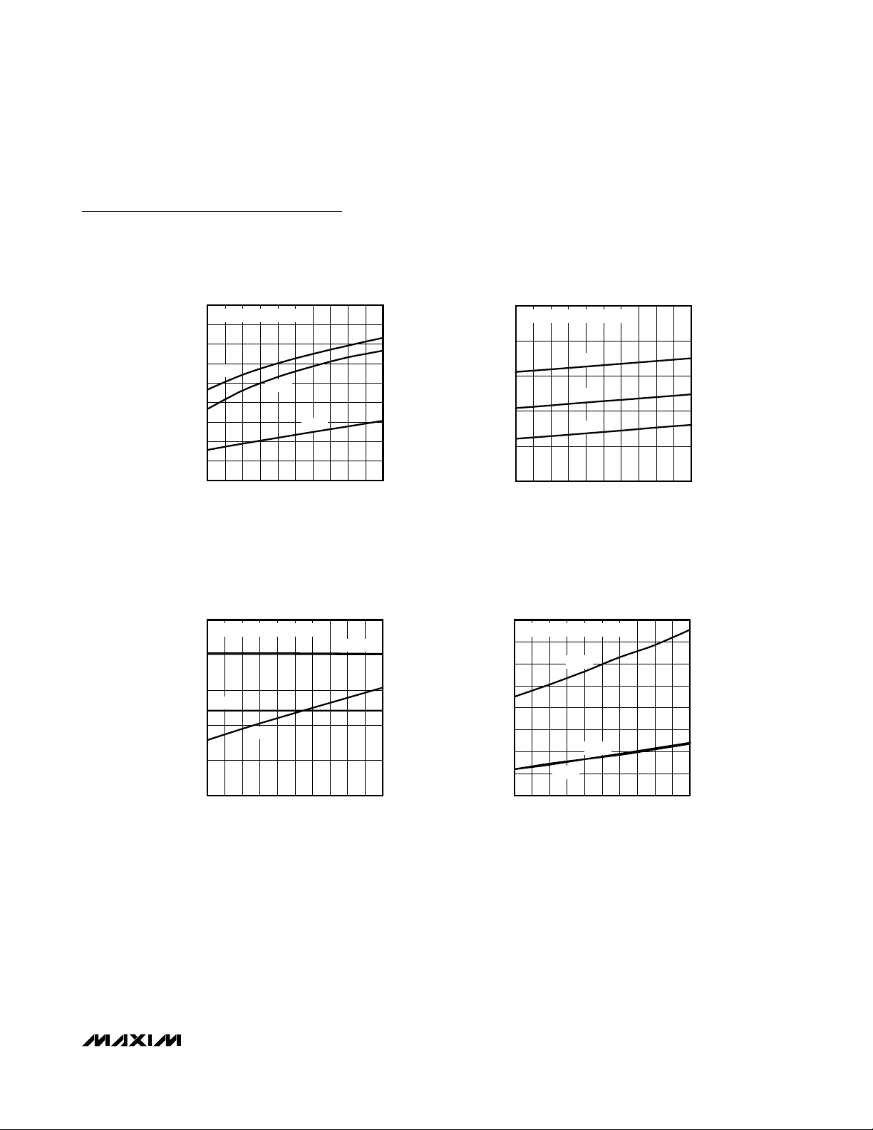
Note 7: For partial power-down and full power-down modes, external clock mode was used for a burst of continuous samples.
Partial power-down or full power-down modes were entered thereafter. By using this method, the conversion rate was found
by averaging the number of conversions over the time starting from the first conversion to the end of the partial power-down
or full power-down modes.
Typical Operating Characteristics (continued)
(AV
DD1
= AV
DD2
= DVDD= DV
DDO
= 5V, AGND1 = DGND = DGNDO = AGND2 = AGND3 = 0, f
CLK
= 3.5MHz (50% duty cycle),
external clock mode, V
REF
= 4.096V (external reference operation), REFCAP = AV
DD1
, maximum single-ended bipolar input range,
C
DOUT
= 50pF, C
SSTRB
= 50pF; unless otherwise noted.)
(mA)
AVDD1
I
ANALOG SUPPLY CURRENT
vs. CONVERSION RATE
3.0
EXTERNAL CLOCK MODE
2.5
2.0
PARTIAL
POWER-DOWN MODE
1.5
1.0
0.5
FULL
POWER-DOWN MODE
MAX1300/01 toc08
PREAMPLIFIER SUPPLY CURRENT
vs. CONVERSION RATE
25
f
= 7.5MHz (NOTE 7)
CLK
20
EXTERNAL CLOCK MODE
FULL POWER-DOWN MODE,
15
PARTIAL POWER-DOWN MODE
(mA)
AVDD2
I
10
5
MAX1300/01 toc09
0
0
CONVERSION RATE (ksps)
DIGITAL SUPPLY CURRENT
vs. CONVERSION RATE
1.8
f
= 7.5MHz (NOTE 7)
CLK
1.6
1.4
EXTERNAL CLOCK MODE,
1.2
PARTIAL POWER-DOWN MODE
1.0
(mA)
0.8
DVDD
I
0.6
0.4
0.2
0
0
FULL POWER-DOWN MODE
15010050
CONVERSION RATE (ksps)
20015010050
MAX1300/01 toc10
200
(mA)
DVDDO
I
0
CONVERSION RATE (ksps)
DIGITAL I/O SUPPLY CURRENT
vs. CONVERSION RATE
0.6
f
= 7.5MHz (NOTE 7)
CLK
0.5
0.4
0.3
0.2
0.1
0
0
EXTERNAL CLOCK MODE
FULL POWER-DOWN MODE,
PARTIAL POWER-DOWN MODE
CONVERSION RATE (ksps)
150100500
200
MAX1300/01 toc11
20015010050
MAX1300/MAX1301
8-/4-Channel, ±12V Multirange Inputs,
Serial 16-Bit ADCs
_______________________________________________________________________________________ 9
Typical Operating Characteristics (continued)
(AV
DD1
= AV
DD2
= DVDD= DV
DDO
= 5V, AGND1 = DGND = DGNDO = AGND2 = AGND3 = 0, f
CLK
= 3.5MHz (50% duty cycle),
external clock mode, V
REF
= 4.096V (external reference operation), REFCAP = AV
DD1
, maximum single-ended bipolar input range,
C
DOUT
= 50pF, C
SSTRB
= 50pF; unless otherwise noted.)
EXTERNAL REFERENCE INPUT CURRENT
vs. EXTERNAL REFERENCE INPUT VOLTAGE
0.16
ALL MODES
0.15
0.14
0.13
EXTERNAL REFERENCE CURRENT (mA)
0.12
3.80 4.15
EXTERNAL REFERENCE VOLTAGE (V)
CHANNEL-TO-CHANNEL ISOLATION
vs. INPUT FREQUENCY
0
f
= 115ksps
SAMPLE
±
12V BIPOLAR RANGE
-20
CH0 TO CH2
-40
-60
ISOLATION (dB)
-80
-100
-120
1 10,000
FREQUENCY (kHz)
2.0
f
±
1.5
1.0
0.5
0
DNL (LSB)
-0.5
-1.0
-1.5
-2.0
0 65,535
GAIN DRIFT vs. TEMPERATURE
0.10
0.08
0.06
MAX1300/01 toc12
0.04
±
0.02
-0.02
GAIN ERROR (%FSR)
-0.04
-0.06
-0.08
MAX1300/01 toc15
CMRR (dB)
-0.10
-10
-20
-30
-40
-50
-60
-70
-80
-90
-100
4.104.054.003.953.903.85
100010010
DIFFERENTIAL NONLINEARITY
vs. DIGITAL OUTPUT CODE
= 115ksps
SAMPLE
12V BIPOLAR RANGE
DIGITAL OUTPUT CODE
0
-40 85
COMMON-MODE REJECTION RATIO
0
f
SAMPLE
±
12V BIPOLAR RANGE
1 10,000
52,42839,32113,107 26,214
12V BIPOLAR RANGE
±
3V BIPOLAR RANGE
TEMPERATURE (°C)
vs. FREQUENCY
= 115ksps
FREQUENCY (kHz)
MAX1300/01 toc18
603510-15
100010010
0
-20
-40
-60
-80
MAGNITUDE (dB)
-100
-120
-140
0
OFFSET DRIFT vs. TEMPERATURE
1.0
0.8
0.6
MAX1300/01 toc13
0.4
0.2
0
-0.2
OFFSET ERROR (mV)
-0.4
-0.6
-0.8
-1.0
±
3V BIPOLAR RANGE
±
12V BIPOLAR RANGE
-40 85
TEMPERATURE (°C)
INTEGRAL NONLINEARITY
vs. DIGITAL OUTPUT CODE
2.0
f
= 115ksps
SAMPLE
±
12V BIPOLAR RANGE
1.5
MAX1300/01 toc16
1.0
0.5
0
INL (LSB)
-0.5
-1.0
-1.5
-2.0
0 65,535
DIGITAL OUTPUT CODE
FFT AT 5kHz
f
= 115ksps
SAMPLE
f
IN(SINE WAVE)
±12V BIPOLAR RANGE
FREQUENCY (kHz)
= 5kHz
MAX1300/01 toc19
5040302010
MAX1300/01 toc14
603510-15
MAX1300/01 toc17
52,42839,32113,107 26,214
MAX1300/MAX1301
8-/4-Channel, ±12V Multirange Inputs,
Serial 16-Bit ADCs
10 ______________________________________________________________________________________
Typical Operating Characteristics (continued)
(AV
DD1
= AV
DD2
= DVDD= DV
DDO
= 5V, AGND1 = DGND = DGNDO = AGND2 = AGND3 = 0, f
CLK
= 3.5MHz (50% duty cycle),
external clock mode, V
REF
= 4.096V (external reference operation), REFCAP = AV
DD1
, maximum single-ended bipolar input range,
C
DOUT
= 50pF, C
SSTRB
= 50pF; unless otherwise noted.)
100
90
80
70
60
50
40
SNR, SINAD (dB)
30
20
10
-20
-40
SNR, SINAD, ENOB
vs. ANALOG INPUT FREQUENCY
SINAD
ENOB
0
1 1000
FREQUENCY (kHz)
MAX1300/01 toc20
SNR
f
= 115ksps
SAMPLE
±12V BIPOLAR RANGE
10010
16
15
14
13
12
11
10
9
8
7
6
ENOB (BITS)
-SFDR, THD vs. SAMPLE RATE
0
f
IN(SINE WAVE)
±12V BIPOLAR RANGE
= 5kHz
MAX1300/01 toc22
SNR, SINAD, ENOB vs. SAMPLE RATE
100
80
60
40
SNR, SINAD (dB)
20
0
SNR, SINAD
ENOB
0.1 1000
SAMPLE RATE (ksps)
-SFDR, THD
vs. ANALOG INPUT FREQUENCY
0
f
= 115ksps
SAMPLE
±12V BIPOLAR RANGE
-20
-40
MAX1300/01 toc21
f
IN(SINE WAVE)
±12V BIPOLAR RANGE
= 5kHz
100101
16
14
12
10
8
6
MAX1300/01 toc23
ENOB (BITS)
-60
-SFDR, THD (dB)
-80
-100
-120
0.1 1000
THD
-SFDR
SAMPLE RATE (ksps)
100101
-60
-SFDR, THD (dB)
-80
THD
-100
-120
1 1000
-SFDR
10010
FREQUENCY (kHz)
ANALOG INPUT CURRENT
1.0
vs. ANALOG INPUT VOLTAGE
ALL MODES
0.6
0.2
-0.2
ANALOG INPUT CURRENT (mA)
-0.6
-1.0
-12 12
ANALOG INPUT VOLTAGE (V)
MAX1300/01 toc24
9630-3-6-9
-10
-15
-20
-25
ATTENUATION (dB)
-30
-35
-40
-45
SMALL-SIGNAL BANDWIDTH
0
-5
1 10,000
FREQUENCY (kHz)
100010010
MAX1300/01 toc25

MAX1300/MAX1301
8-/4-Channel, ±12V Multirange Inputs,
Serial 16-Bit ADCs
______________________________________________________________________________________ 11
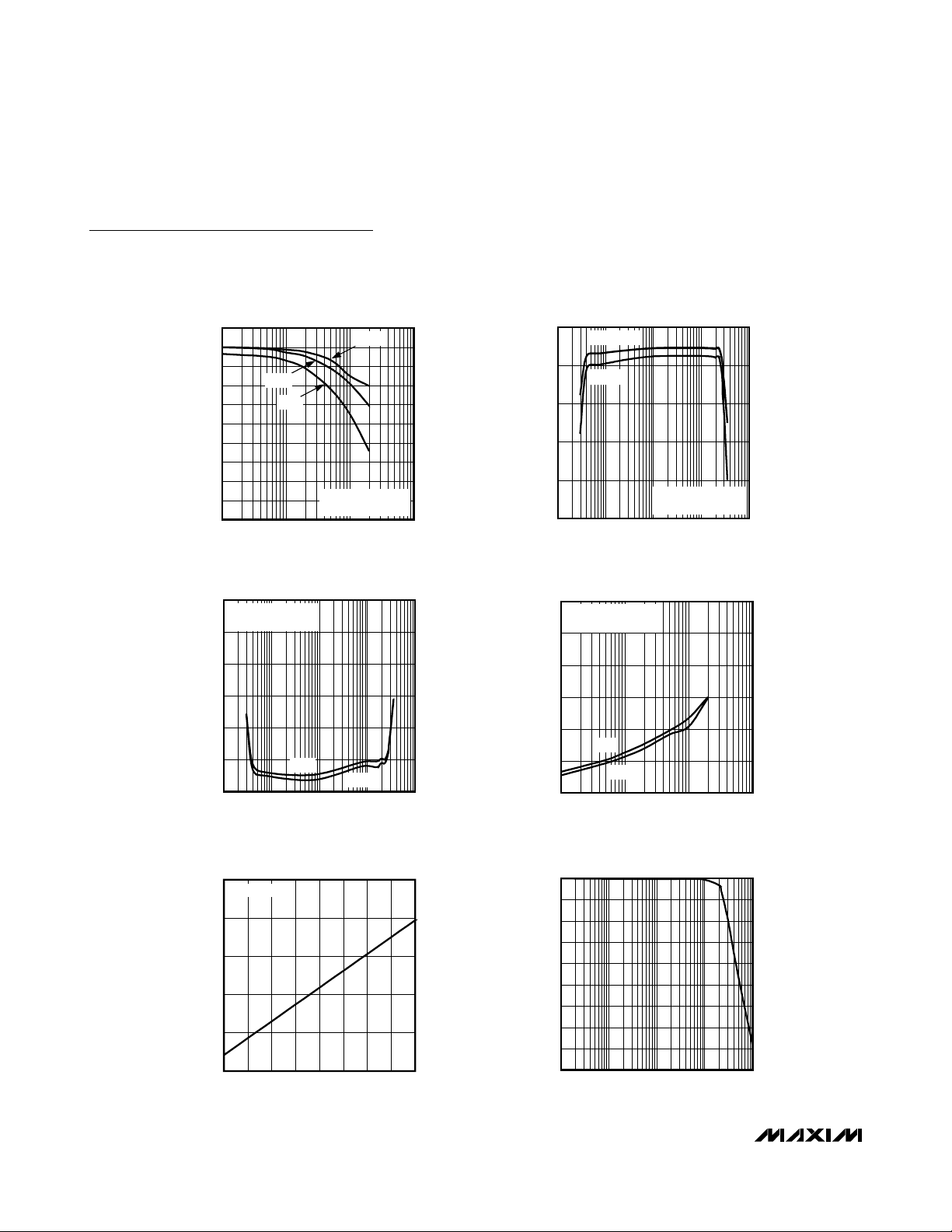
Typical Operating Characteristics (continued)
(AV
DD1
= AV
DD2
= DVDD= DV
DDO
= 5V, AGND1 = DGND = DGNDO = AGND2 = AGND3 = 0, f
CLK
= 3.5MHz (50% duty cycle),
external clock mode, V
REF
= 4.096V (external reference operation), REFCAP = AV
DD1
, maximum single-ended bipolar input range,
C
DOUT
= 50pF, C
SSTRB
= 50pF; unless otherwise noted.)
REFERENCE VOLTAGE vs. TIME
MAX1300/01 toc27
1V/div
0V
4ms/div
ATTENUATION (dB)
35,000
30,000
25,000
20,000
15,000
NUMBER OF HITS
10,000
5,000
FULL-POWER BANDWIDTH
0
-5
-10
-15
-20
-25
-30
-35
-40
-45
1 10,000
FREQUENCY (kHz)
100010010
NOISE HISTOGRAM
(CODE EDGE)
65,534 SAMPLES
0
32,785 32,789
32,787
32,786 32,788 32,790
CODE
MAX1300/01 toc26
MAX1300/01 toc28
40,000
65,534 SAMPLES
35,000
30,000
25,000
20,000
15,000
NUMBER OF HITS
10,000
5,000
0
NOISE HISTOGRAM
(CODE CENTER)
MAX1300/01 toc29
32,77732,775
CODE
32,778
32,779
32,78032,774
32,776

MAX1300/MAX1301
8-/4-Channel, ±12V Multirange Inputs,
Serial 16-Bit ADCs
12 ______________________________________________________________________________________
Pin Description
PIN
MAX1300 MAX1301
12AV
2 3 CH0 Analog Input Channel 0
3 4 CH1 Analog Input Channel 1
4 5 CH2 Analog Input Channel 2
5 6 CH3 Analog Input Channel 3
6 — CH4 Analog Input Channel 4
7 — CH5 Analog Input Channel 5
8 — CH6 Analog Input Channel 6
9 — CH7 Analog Input Channel 7
10 7 CS
11 8 DIN
12 9 SSTRB
13 10 SCLK
14 11 DOUT
15 12 DGNDO Digital I/O Ground. DGND, DGNDO, AGND3, AGND2, and AGND1 must be connected together.
16 13 DGND Digital Ground. DGND, DGNDO, AGND3, AGND2, and AGND1 must be connected together.
17 14 DV
18 15 DV
19 16 REFCAP
NAME FUNCTION
Analog Supply Voltage 1. Connect AV
DD1
DDO
DD
to AGND1 with a 0.1µF capacitor.
AV
DD1
Active-Low Chip-Select Input. When CS is low, data is clocked into the device from DIN on the
rising edge of SCLK. With CS low, data is clocked out of DOUT on the falling edge of SCLK.
When CS is high, activity on SCLK and DIN is ignored and DOUT is high impedance.
Serial Data Input. When CS is low, data is clocked in on the rising edge of SCLK. When CS is
high, transitions on DIN are ignored.
Serial-Strobe Output. When using the internal clock, SSTRB rising edge transitions indicate that
data is ready to be read from the device. When operating in external clock mode, SSTRB is
always low. SSTRB does not tri-state, regardless of the state of CS, and therefore requires
a dedicated I/O line.
Serial Clock Input. When CS is low, transitions on SCLK clock data into DIN and out of DOUT.
When CS is high, transitions on SCLK are ignored.
Serial Data Output. When CS is low, data is clocked out of DOUT with each falling SCLK
transition. When CS is high, DOUT is high impedance.
Digital I/O Supply Voltage Input. Connect DV
Bypass DV
Digital-Supply Voltage Input. Connect DVDD to a +4.75V to +5.25V power-supply voltage.
Bypass DV
Bandgap-Voltage Bypass Node. For external reference operation, connect REFCAP to AV
For internal reference operation, bypass REFCAP with a 0.01µF capacitor to AGND1
(V
REFCAP
DDO
DD
≈ 4.096V).
to a +4.75V to +5.25V power-supply voltage. Bypass
DD1
to DGNDO with a 0.1µF capacitor.
to DGND with a 0.1µF capacitor.
DDO
to a +2.7V to +5.25V power-supply voltage.
DD
.
Reference-Buffer Output/ADC Reference Input. For external reference operation, apply an
20 17 REF
external reference voltage from 3.800V to 4.136V to REF. For internal reference operation,
bypassing REF with a 1µF capacitor to AGND1 sets V
= 4.096V ±1%.
REF

Detailed Description
The MAX1300/MAX1301 multirange, low-power, 16-bit
successive-approximation ADCs operate from a single
+5V supply and have a separate digital supply allowing
digital interface with 2.7V to 5.25V systems. These 16-bit
ADCs have internal track-and-hold (T/H) circuitry that
supports single-ended and fully differential inputs. For
single-ended conversions, the valid analog input voltage
range spans from -12V below ground to +12V above
ground. The maximum allowable differential input voltage spans from -24V to +24V. Data can be converted in
a variety of software-programmable channel and dataacquisition configurations. Microprocessor (µP) control is
made easy through an SPI-/QSPI-/MICROWIRE-compatible serial interface.
The MAX1300 has eight single-ended analog input
channels or four differential channels (see the Block
Diagram at the end of the data sheet). The MAX1301
has four single-ended analog input channels or two differential channels. Each analog input channel is independently software programmable for seven
single-ended input ranges (0 to +6V, -6V to 0, 0 to
+12V, -12V to 0, ±3V, ±6V, and ±12V) and three differential input ranges (±6V, ±12V, and ±24V).
Additionally, all analog input channels are fault tolerant
to ±16.5V. A fault condition on an idle channel does not
affect the conversion result of other channels.
MAX1300/MAX1301
8-/4-Channel, ±12V Multirange Inputs,
Serial 16-Bit ADCs
______________________________________________________________________________________ 13
Pin Description (continued)
Figure 1. Typical Application Circuit
PIN
MAX1300 MAX1301
21 18 AGND3
22 19 AV
23 20 AGND2
24 1 AGND1 Analog Ground 1. DGND, DGNDO, AGND3, AGND2, and AGND1 must be connected together.
NAME FUNCTION
Analog Signal Ground 3. AGND3 is the ADC negative reference potential. Connect AGND3 to
AGND1. DGND, DGNDO, AGND3, AGND2, and AGND1 must be connected together.
Analog Supply Voltage 2. Connect AV
DD2
to AGND2 with a 0.1µF capacitor.
AV
DD2
to a +4.75V to +5.25V power-supply voltage. Bypass
DD2
Analog Ground 2. This ground carries approximately five times more current than AGND1.
DGND, DGNDO, AGND3, AGND2, and AGND1 must be connected together.
5.0V 5.0V 5.0V
0.1µF 0.1µF 0.1µF
ACCELERATION
1µF
4–20mA
PLC
PRESSURE
TEMPERATURE
WHEATESTONE
WHEATESTONE
0.1µF
AV
CHO
CH1
CH2
CH3
CH4
CH5
CH6
CH7
REF
AGND1
REFCAP
AGND2
DD2
AV
DD1
MAX1300
DGNDOAGND3 DGND
DV
DD
DV
SCLK
SSTRB
DOUT
3.3V
DDO
0.1µF
CS
DIN
V
DD
MC68HCXX
µC
SCK
I/O
MOSI
I/O
MISO
V
SS

MAX1300/MAX1301
Power Supplies
To maintain a low-noise environment, the MAX1300 and
MAX1301 provide separate power supplies for each
section of circuitry. Table 1 shows the four separate
power supplies. Achieve optimal performance using
separate AV
DD1
, AV
DD2
, DVDD, and DV
DDO
supplies.
Alternatively, connect AV
DD1
, AV
DD2
, and DV
DD
together as close to the device as possible for a convenient power connection. Connect AGND1, AGND2,
AGND3, DGND, and DGNDO together as close to the
device as possible. Bypass each supply to the corresponding ground using a 0.1µF capacitor (Table 1). If
significant low-frequency noise is present, add a 10µF
capacitor in parallel with the 0.1µF bypass capacitor.
Converter Operation
The MAX1300/MAX1301 ADCs feature a fully differential, successive-approximation register (SAR) conversion technique and an on-chip T/H block to convert
voltage signals into a 16-bit digital result. Both singleended and differential configurations are supported
with programmable unipolar and bipolar signal ranges.
Track-and-Hold Circuitry
The MAX1300/MAX1301 feature a switched-capacitor
T/H architecture that allows the analog input signal to be
stored as charge on sampling capacitors. See Figures 2,
3, and 4 for T/H timing and the sampling instants for
each operating mode. The MAX1300/MAX1301 analog
input circuitry buffers the input signal from the sampling
capacitors, resulting in a constant input impedance with
varying input voltage (Figure 5).
Analog Input Circuitry
Select differential or single-ended conversions using the
associated analog input configuration byte (Table 2).
The analog input signal source must be capable of driving the ADC’s 17kΩ input resistance (Figure 6).
Figure 6 shows the simplified analog input circuit. The
analog inputs are ±16.5V fault tolerant and are protected
by back-to-back diodes. The summing junction voltage,
VSJ, is a function of the channel’s input commonmode voltage:
As a result, the analog input impedance is relatively constant over input voltage as shown in Figure 5.
8-/4-Channel, ±12V Multirange Inputs,
Serial 16-Bit ADCs
14 ______________________________________________________________________________________
Table 1. MAX1300/MAX1301 Power Supplies and Bypassing
Table 2. Analog Input Configuration Byte
V
⎛
⎜
SJ CM
⎝
POWER
SUPPLY/GROUND
DV
/DGNDO 2.7 to 5.25 0.2 Digital I/O 0.1µF to DGNDO
DDO
AV
/AGND2 4.75 to 5.25 17.5 Analog Circuitry 0.1µF to AGND2
DD2
AV
/AGND1 4.75 to 5.25 3.0 Analog Circuitry 0.1µF to AGND1
DD1
DVDD/DGND 4.75 to 5.25 0.9 Digital Control Logic and Memory 0.1µF to DGND
SUPPLY VOLTAGE
RANGE (V)
TYPICAL SUPPLY
CURRENT (mA)
R
1
⎞
.
×++
2 375 1
⎟
⎠
+
RR
12
CIRCUIT SECTION BYPASSING
⎛
⎜
⎝
⎛
⎜
⎝
RR
12
V
R
1
+
⎞
⎞
=
⎟
⎟
⎠
⎠
V
×
BIT
NUMBER
7 START Start Bit. The first logic 1 after CS goes low defines the beginning of the analog input configuration byte.
6C2
5C1
4C0
3 DIF/SGL
2R2
1R1
0R0
NAME DESCRIPTION
Channel-Select Bits. SEL[2:0] select the analog input channel to be configured (Tables 4 and 5).
Differential or Single-Ended Configuration Bit. DIF/SGL = 0 configures the selected analog input channel
for single-ended operation. DIF/SGL = 1 configures the channel for differential operation. In single-ended
mode, input voltages are measured between the selected input channel and AGND1, as shown in
Table 4. In differential mode, the input voltages are measured between two input channels, as shown in
Table 5. Be aware that changing DIF/SGL adjusts the FSR, as shown in Table 6.
Input-Range-Select Bits. R[2:0] select the input voltage range, as shown in Table 6 and Figure 7.

Single-ended conversions are internally referenced to
AGND1 (Tables 3 and 4). In differential mode, IN+ and
IN- are selected according to Tables 3 and 5. When configuring differential channels, the differential pair follows
the analog configuration byte for the positive channel.
For example, to configure CH2 and CH3 for a ±12V differential conversion, set the CH2 analog configuration
byte for a differential conversion with the ±12V range
(1010 1100). To initiate a conversion for the CH2 and
CH3 differential pair, issue the command 1010 0000.
Analog Input Bandwidth
The MAX1300/MAX1301 input-tracking circuitry has a
2MHz small-signal bandwidth. The 2MHz input bandwidth makes it possible to digitize high-speed transient
events. Harmonic distortion increases when digitizing
signal frequencies above 15kHz as shown in the THD
and -SFDR vs. Input Frequency plot in the Typical
Operating Characteristics.
Analog Input Range and Fault Tolerance
Figure 7 illustrates the software-selectable single-ended
analog input voltage range that produces a valid digital
output. Each analog input channel can be independently
programmed to one of seven single-ended input ranges
by setting the R[2:0] control bits with DIF/SGL = 0.
MAX1300/MAX1301
8-/4-Channel, ±12V Multirange Inputs,
Serial 16-Bit ADCs
______________________________________________________________________________________ 15
Figure 2. External Clock-Mode Conversion (Mode 0)
CS
1
2
3
4
SCLK
SSTRB
DIN S C2 C1 C0 0 0 0 0
ANALOG INPUT
TRACK AND HOLD*
HOLD TRACK HOLD
5
BYTE 1 BYTE 2 BYTE 3 BYTE 4
10
11
12
13
14
15
16
6
7
8
9
f
SAMPLE
t
ACQ
171819
≈ f
/ 32
SCLK
SAMPLING INSTANT
20
21
22
232425
26
27
28
29
303132
HIGH
DOUT
IMPEDANCE
*TRACK AND HOLD TIMING IS CONTROLLED BY SCLK.
B15 B14 B13 B12 B11 B10 B9 B8 B7 B6 B5 B4 B3 B2 B1 B0
HIGH
IMPEDANCE

MAX1300/MAX1301
Figure 8 illustrates the software-selectable differential
analog input voltage range that produces a valid digital
output. Each analog input differential pair can be independently programmed to one of three differential input
ranges by setting the R[2:0] control bits with DIF/SGL = 1.
Regardless of the specified input voltage range and
whether the channel is selected, each analog input is
±16.5V fault tolerant. The analog input fault protection
is active whether the device is unpowered or powered.
Any voltage beyond FSR, but within the ±16.5V faulttolerant range, applied to an analog input results in a
full-scale output voltage for that channel.
Clamping diodes with breakdown thresholds in excess
of 16.5V protect the MAX1300/MAX1301 analog inputs
during ESD and other transient events (Figure 6). The
clamping diodes do not conduct during normal device
operation, nor do they limit the current during such
transients. When operating in an environment with the
potential for high-energy voltage and/or current transients, protect the MAX1300/MAX1301 externally.
8-/4-Channel, ±12V Multirange Inputs,
Serial 16-Bit ADCs
16 ______________________________________________________________________________________
Figure 3. External Acquisition-Mode Conversion (Mode 1)
CS
SSTRB
SCLK
DIN SC2C1C00000
DOUT
123
4
56789
BYTE 1 BYTE 2 BYTE 3 BYTE 4
10111213141516
t
ANALOG INPUT
TRACK AND HOLD*
INTCLK**
HOLD
*TRACK AND HOLD TIMING IS CONTROLLED BY SCLK.
**INTCLK IS AN INTERNAL SIGNAL AND IS NOT ACCESSIBLE TO THE USER.
ACQ
TRACK HOLD
f
SAMPLE
SAMPLING INSTANT
100ns to 400ns
123
171819202122232425262728293031
f
≈ f
INTCLK
SCLK
/ 32 + f
≈ 4.5MHz
HIGH IMPEDANCE
/ 17
INTCLK
141516
B15 B14 B13 B12 B11 B10 B9 B8 B7 B6 B5 B4 B3 B2 B1 B0
17
32

Figure 6. Simplified Analog Input Circuit
MAX1300/MAX1301
8-/4-Channel, ±12V Multirange Inputs,
Serial 16-Bit ADCs
______________________________________________________________________________________ 17
SSTRB
Figure 4. Internal Clock-Mode Conversion (Mode 2)
Figure 5. Analog Input Current vs. Input Voltage
CS
SCLK
DOUT
ANALOG INPUT
TRACK AND HOLD*
INTCLK**
1234567
DIN S C2 C1 C0 0 0 0 0
HOLD HOLD
BYTE 1 BYTE 2 BYTE 3
*TRACK AND HOLD TIMING IS CONTROLLED BY INTCLK, AND IS NOT ACCESSIBLE TO THE USER.
**INTCLK IS AN INTERNAL SIGNAL AND IS NOT ACCESSIBLE TO THE USER.
8
t
ACQ
TRACK
100ns to 400ns
123
1.0
ALL MODES
0.6
0.2
-0.2
ANALOG INPUT CURRENT (mA)
-0.6
-1.0
-12 12
ANALOG INPUT VOLTAGE (V)
9630-3-6-9
HIGH IMPEDANCE
f
f
SAMPLE
SAMPLING INSTANT
1011121314
≈ 4.5MHz
INTCLK
10111213141516
9
B15 B14 B13 B12 B11 B10 B9 B8 B7 B6 B5 B4 B3 B2 B1 B0
≈ f
/ 24 + f
/ 28
SCLK
INTCLK
252627
28
MAX1300
17181920212223
R2
24
MAX1301
*R
SOURCE
ANALOG
SIGNAL
SOURCE
*R
SOURCE
ANALOG
SIGNAL
SOURCE
IN_+
IN_+
R1
V
SJ
R2
R1
V
SJ
*MINIMIZE R
TO AVOID GAIN ERROR AND DISTORTION.
SOURCE

MAX1300/MAX1301
Differential Common-Mode Range
The MAX1300/MAX1301 differential common-mode
range (V
CMDR
) must remain within -14V to +10V to obtain
valid conversion results. The differential common-mode
range is defined as:
In addition to the common-mode input voltage limitations,
each individual analog input must be limited to ±16.5V
with respect to AGND1.
The range-select bits R[2:0] in the analog input configuration bytes determine the full-scale range for the corresponding channel (Tables 2 and 6). Figures 9, 10,
and 11 show the valid analog input voltage ranges for
the MAX1300/MAX1301 when operating with FSR =
12V, FSR = 24V, and FSR = 48V, respectively. The
shaded area contains the valid common-mode voltage
ranges that support the entire FSR.
8-/4-Channel, ±12V Multirange Inputs,
Serial 16-Bit ADCs
18 ______________________________________________________________________________________
Table 3. Input Data Word Formats
Table 4. Channel Selection in Single-Ended Mode (DIF/
SSGGLL
= 0)
Table 5. Channel Selection in True-Differential Mode (DIF/
SSGGLL
= 1)
DATA BIT
OPERATION
Conversion-Start Byte
(Tables 4 and 5)
Analog-Input Configuration Byte
(Table 2)
Mode-Control Byte
(Table 7)
D7
(START)
1C2C1C00000
1 C2 C1 C0 DIF/SGL R2 R1 R0
1M2M1M01000
D6 D5 D4 D3 D2 D1 D0
CHANNEL-SELECT BIT CHANNEL
C2 C1 C0 CH0 CH1 CH2 CH3 CH4 CH5 CH6 CH7 AGND1
000+ -
001 + -
010 + -
011 + -
100 + -
101 + -
110 +-
111 +-
CHANNEL-SELECT BIT CHANNEL
C2 C1 C0 CH0 CH1 CH2 CH3 CH4 CH5 CH6 CH7 AGND1
000+-
0 0 1 RESERVED
010 +-
0 1 1 RESERVED
100 +-
1 0 1 RESERVED
110 +-
1 1 1 RESERVED
CH CH
_ _
+
V
CMDR
()
=
+
2
−
()

Digital Interface
The MAX1300/MAX1301 feature a serial interface that is
compatible with SPI/QSPI and MICROWIRE devices.
DIN, DOUT, SCLK, CS, and SSTRB facilitate bidirectional communication between the MAX1300/MAX1301
and the master at SCLK rates up to 10MHz (internal
clock mode, mode 2), 3.67MHz (external clock mode,
mode 0), or 4.39MHz (external acquisition mode, mode
1). The master, typically a microcontroller, should use
the CPOL = 0, CPHA = 0, SPI transfer format, as shown
in the timing diagrams of Figures 2, 3, and 4.
The digital interface is used to:
• Select single-ended or true-differential input channel
configurations
• Select the unipolar or bipolar input range
• Select the mode of operation:
External clock (mode 0)
External acquisition (mode 1)
Internal clock (mode 2)
Reset (mode 4)
Partial power-down (mode 6)
Full power-down (mode 7)
• Initiate conversions and read results
Chip Select
(CS)
CS enables communication with the MAX1300/MAX1301.
When CS is low, data is clocked into the device from DIN
on the rising edge of SCLK and data is clocked out of
DOUT on the falling edge of SCLK. When CS is high,
activity on SCLK and DIN is ignored and DOUT is high
impedance allowing DOUT to be shared with other
peripherals. SSTRB is never high impedance and therefore cannot be shared with other peripherals.
Serial Strobe Output (SSTRB)
As shown in Figures 3 and 4, the SSTRB transitions high
to indicate that the ADC has completed a conversion
and results are ready to be read by the master. SSTRB
remains low in the external clock mode (Figure 2) and
consequently may be left unconnected. SSTRB is driven
high or low regardless of the state of CS, therefore
SSTRB cannot be shared with other peripherals.
MAX1300/MAX1301
8-/4-Channel, ±12V Multirange Inputs,
Serial 16-Bit ADCs
______________________________________________________________________________________ 19
Figure 7. Single-Ended Input Voltage Ranges
Figure 8. Differential Input Voltage Ranges
+12
+9
+6
FSR = 12V
+3
0
FSR = 6V
(CH_) - AGND1 (V)
-3
-6
-9
-12
001
EACH INPUT IS FAULT TOLERANT TO ±16.5V.
V
= 4.096V.
REF
FSR = 6V
FSR = 12V
FSR = 6V
FSR = 12V
010
011
100
INPUT RANGE SELECTION BITS, R[2:0]
101
110
FSR = 24V
111
+24
+18
+12
+6
0
FSR = 12V
(CH_+) - (CH_-) (V)
-6
-12
-18
-24
001
010
INPUT RANGE SELECTION BITS, R[2:0]
EACH INPUT IS FAULT TOLERANT TO ±16.5V.
V
= 4.096V.
REF
011
FSR = 24V
100
101
110
FSR = 48V
111

MAX1300/MAX1301
8-/4-Channel, ±12V Multirange Inputs,
Serial 16-Bit ADCs
20 ______________________________________________________________________________________
Table 6. Range-Select Bits
*Conversion-Start Byte (see Table 3).
**Mode-Control Byte (see Table 3).
DIF/SGL R2 R1 R0 MODE TRANSFER FUNCTION
0 0 0 0 No Range Change* —
Single-Ended
0001
0010
0011
0100
0101
Bipolar -3V to +3V
Full-Scale Range (FSR) = 6V
Single-Ended
Unipolar -6V to 0
FSR = 6V
Single-Ended
Unipolar 0 to +6V
FSR = 6V
Single-Ended
Bipolar -6V to +6V
FSR = 12V
Single-Ended
Unipolar -12V to 0
FSR = 12V
Figure 12
Figure 13
Figure 14
Figure 12
Figure 13
Single-Ended
0110
0111
1 0 0 0 No Range Change** —
1001
1 0 1 0 Reserved —
1 0 1 1 Reserved —
1100
1 1 0 1 Reserved —
1 1 1 0 Reserved —
1111
Unipolar 0 to +12V
FSR = 12V
DEFAULT SETTING
Single-Ended
Bipolar -12V to +12V
FSR = 24V
Differential
Bipolar -6V to +6V
FSR = 12V
Differential
Bipolar -12V to +12V
FSR = 24V
Differential
Bipolar -24V to +24V
FSR = 48V
Figure 14
Figure 12
Figure 12
Figure 12
Figure 12

Start Bit
Communication with the MAX1300/MAX1301 is accomplished using the three input data word formats shown
in Table 3. Each input data word begins with a start bit.
The start bit is defined as the first high bit clocked into
DIN with CS low when any of the following are true:
• Data conversion is not in process and all data from
the previous conversion has clocked out of DOUT.
• The device is configured for operation in external
clock mode (mode 0) and previous conversion-result
bits B15–B3 have clocked out of DOUT.
• The device is configured for operation in external
acquisition mode (mode 1) and previous conversionresult bits B15–B7 have clocked out of DOUT.
• The device is configured for operation in internal
clock mode, (mode 2) and previous conversionresult bits B15–B4 have clocked out of DOUT.
Output Data Format
Output data is clocked out of DOUT in offset binary format on the falling edge of SCLK, MSB first (B15). For
output binary codes, see the Transfer Function section
and Figures 12, 13, and 14.
Configuring Analog Inputs
Each analog input has two configurable parameters:
• Single-ended or true-differential input
• Input voltage range
These parameters are configured using the analog input
configuration byte as shown in Table 2. Each analog
input has a dedicated register to store its input configuration information. The timing diagram of Figure 15 shows
how to write to the analog input configuration registers.
Figure 16 shows DOUT and SSTRB timing.
Transfer Function
An ADC’s transfer function defines the relationship
between the analog input voltage and the digital output
code. Figures 12, 13, and 14 show the MAX1300/
MAX1301 transfer functions. The transfer function is
determined by the following characteristics:
• Analog input voltage range
• Single-ended or differential configuration
• Reference voltage
The axes of an ADC transfer function are typically in least
significant bits (LSBs). For the MAX1300/MAX1301, an
LSB is calculated using the following equation:
where N is the number of bits (N = 16) and FSR is the
full-scale range (see Figures 7 and 8).
MAX1300/MAX1301
8-/4-Channel, ±12V Multirange Inputs,
Serial 16-Bit ADCs
______________________________________________________________________________________ 21
Figure 9. Common-Mode Voltage vs. Input Voltage (FSR = 12V)
Figure 10. Common-Mode Voltage vs. Input Voltage (FSR = 24V)
Figure 11. Common-Mode Voltage vs. Input Voltage (FSR = 48V)
12
8
4
0
-4
-8
COMMON-MODE VOLTAGE (V)
-12
-16
-18 18
INPUT VOLTAGE (V)
12
8
4
0
-4
-8
COMMON-MODE VOLTAGE (V)
-12
-16
-18 18
INPUT VOLTAGE (V)
1260-6-12
1260-6-12
12
8
4
0
-4
-8
COMMON-MODE VOLTAGE (V)
-12
-16
-18 18
INPUT VOLTAGE (V)
1260-6-12
FSR V
×
.
×
REF
V
1
LSB
=
N
2 4 096

MAX1300/MAX1301
Mode Control
The MAX1300/MAX1301 contain one byte-wide modecontrol register. The timing diagram of Figure 15 shows
how to use the mode-control byte, and the mode-control byte format is shown in Table 7. The mode-control
byte is used to select the conversion method and to
control the power modes of the MAX1300/MAX1301.
Selecting the Conversion Method
The conversion method is selected using the mode-control byte (see the Mode Control section), and the conversion is initiated using a conversion-start command (Table
3, and Figures 2, 3, and 4).The MAX1300/MAX1301 convert analog signals to digital data using one of three
methods:
• External Clock Mode, Mode 0 (Figure 2)
• Highest maximum throughput (see the Electrical
Characteristics table)
• User controls the sample instant
• CS remains low during the conversion
• User supplies SCLK throughout the ADC conversion and reads data at DOUT
• External Acquisition Mode, Mode 1 (Figure 3)
• Lowest maximum throughput (see the Electrical
Characteristics table)
• User controls the sample instant
• User supplies two bytes of SCLK, then drives
CS high to relieve processor load while the ADC
converts
• After SSTRB transitions high, the user supplies
two bytes of SCLK and reads data at DOUT
• Internal Clock Mode, Mode 2 (Figure 4)
• High maximum throughput (see the Electrical
Characteristics table)
• The internal clock controls the sampling instant
8-/4-Channel, ±12V Multirange Inputs,
Serial 16-Bit ADCs
22 ______________________________________________________________________________________
Figure 13. Ideal Unipolar Transfer Function, Single-Ended
Input, -FSR to 0
Figure 14. Ideal Unipolar Transfer Function, Single-Ended
Input, 0 to +FSR
Figure 12. Ideal Bipolar Transfer Function, Single-Ended or
Differential Input
FFFF
FFFE
FFFD
8001
8000
7FFF
BINARY OUTPUT CODE (LSB [hex])
0003
0002
0001
0000
-32,768 -32,766 0 +32,765 +32,767
INPUT VOLTAGE (LSB [DECIMAL])
FSR
1 LSB =
-1 +1
AGND1 (DIF/SGL = 0)
OV (DIF/SGL = 1)
FSR x V
REF
65,536 x 4.096V
FFFF
FFFE
FFFD
8001
8000
7FFF
BINARY OUTPUT CODE (LSB [hex])
0003
0002
0001
0000
0 1 2 3 32,768 65,533 65,535
(AGND1)
INPUT VOLTAGE (LSB [DECIMAL])
FSR
1 LSB =
FSR x V
REF
65,536 x 4.096V
FSR
FSR
FFFF
FFFE
FFFD
8001
8000
7FFF
BINARY OUTPUT CODE (LSB [hex])
0003
0002
0001
0000
0 1 2 3 32,768 65,533 65,535
INPUT VOLTAGE (LSB [DECIMAL])
FSR
1 LSB =
FSR x V
REF
65,536 x 4.096V
FSR
(AGND1)

• User supplies one byte of SCLK, then drives CS
high to relieve processor load while the ADC
converts
• After SSTRB transitions high, the user supplies
two bytes of SCLK and reads data at DOUT
External Clock Mode (Mode 0)
The MAX1300/MAX1301’s fastest maximum throughput
rate is achieved operating in external clock mode.
SCLK controls both the acquisition and conversion of
the analog signal, facilitating precise control over when
the analog signal is captured. The analog input sampling instant is at the falling edge of the 14th SCLK
(Figure 2).
Since SCLK drives the conversion in external clock
mode, the SCLK frequency should remain constant
while the conversion is clocked. The minimum SCLK
frequency prevents droop in the internal sampling
capacitor voltages during conversion.
SSTRB remains low in the external clock mode, and as a
result may be left unconnected if the MAX1300/
MAX1301 will always be used in the external clock mode.
MAX1300/MAX1301
8-/4-Channel, ±12V Multirange Inputs,
Serial 16-Bit ADCs
______________________________________________________________________________________ 23
Figure 15. Analog Input Configuration Byte and Mode-Control Byte Timing
Figure 16. DOUT and SSTRB Timing
Table 7. Mode-Control Byte
t
HIGH
IMPEDANCE
CSPW
SCLK
DOUT
CS
DIN
t
CSS
t
DS
t
DV
HIGH
IMPEDANCE
t
CL
18
START
SEL2
SEL1 SEL0 R2 R1
ANALOG INPUT CONFIGURATION BYTE
t
CP
t
DIF/SGL
CH
t
CSH
t
DH
R0
t
TR
SSTRB
t
SSCS
SCLK
DOUT
CS
t
CSS
t
DO
HIGH
IMPEDANCE
MSB
NOTE:
SSTRB AND CS REMAIN LOW IN EXTERNAL CLOCK MODE (MODE 0).
18
START
M2
M1 M0 1 0 0
MODE CONTROL BYTE
0
HIGH
IMPEDANCE
BIT NUMBER BIT NAME DESCRIPTION
7 START Start Bit. The first logic 1 after CS goes low defines the beginning of the mode-control byte.
6M2
5M1
4M0
3 1 Bit 3 must be a logic 1 for the mode-control byte.
2 0 Bit 2 must be a logic 0 for the mode-control byte.
1 0 Bit 1 must be a logic 0 for the mode-control byte.
0 0 Bit 0 must be a logic 0 for the mode-control byte.
Mode-Control Bits. M[2:0] select the mode of operation as shown in Table 8.

MAX1300/MAX1301
External Acquisition Mode (Mode 1)
The slowest maximum throughput rate is achieved with
the external acquisition method. SCLK controls the
acquisition of the analog signal in external acquisition
mode, facilitating precise control over when the analog
signal is captured. The internal clock controls the conversion of the analog input voltage. The analog input
sampling instant is at the falling edge of the 16th SCLK
(Figure 3).
For the external acquisition mode, CS must remain low
for the first 15 clock cycles and the rise on or after the
falling edge of the 16th SCLK cycle as shown in Figure
3. For optimal performance, idle DIN and SCLK during
the conversion. With careful board layout, transitions at
DIN and SCLK during the conversion have a minimal
impact on the conversion result.
After the conversion is complete, SSTRB asserts high
and CS can be brought low to read the conversion
result. SSTRB returns low on the rising SCLK edge of
the subsequent start bit.
Internal Clock Mode (Mode 2)
In internal clock mode, the internal clock controls both
acquisition and conversion of the analog signal. The internal clock starts approximately 100ns to 400ns after the
falling edge of the eighth SCLK and has a rate of about
4.5MHz. The analog input sampling instant occurs at the
falling edge of the 11th internal clock signal (Figure 4).
For the internal clock mode, CS must remain low for the
first seven SCLK cycles and then rise on or after the
falling edge of the eighth SCLK cycle. After the conversion is complete, SSTRB asserts high and CS can be
brought low to read the conversion result. SSTRB returns
low on the rising SCLK edge of the subsequent start bit.
Reset (Mode 4)
As shown in Table 8, set M[2:0] = 100 to reset the
MAX1300/MAX1301 to its default conditions. The
default conditions are full power operation with each
channel configured for ±12V, bipolar, single-ended
conversions using external clock mode (mode 0).
Partial Power-Down Mode (Mode 6)
As shown in Table 8, when M[2:0] = 110, the device
enters partial power-down mode. In partial powerdown, all analog portions of the device are powered
down except for the reference voltage generator and
bias supplies.
To exit partial power-down, change the mode by issuing one of the following mode-control bytes (see the
Mode Control section):
• External-Clock-Mode Control Byte
• External-Acquisition-Mode Control Byte
• Internal-Clock-Mode Control Byte
• Reset Byte
• Full Power-Down-Mode Control Byte
This prevents the MAX1300/MAX1301 from inadvertently exiting partial power-down mode because of a CS
glitch in a noisy digital environment.
Full Power-Down Mode (Mode 7)
When M[2:0] = 111, the device enters full power-down
mode and the total supply current falls to 1µA (typ). In
full power-down, all analog portions of the device are
powered down. When using the internal reference,
upon exiting full power-down mode, allow 10ms for the
internal reference voltage to stabilize prior to initiating a
conversion.
To exit full power-down, change the mode by issuing
one of the following mode-control bytes (see the Mode
Control section):
• External-Clock-Mode Control Byte
8-/4-Channel, ±12V Multirange Inputs,
Serial 16-Bit ADCs
24 ______________________________________________________________________________________
Table 8. Mode-Control Bits M[2:0]
M2 M1 M0 MODE
0 0 0 External Clock (DEFAULT)
0 0 1 External Acquisition
0 1 0 Internal Clock
0 1 1 Reserved
1 0 0 Reset
1 0 1 Reserved
1 1 0 Partial Power-Down
1 1 1 Full Power-Down

• External-Acquisition-Mode Control Byte
• Internal-Clock-Mode Control Byte
• Reset Byte
• Partial Power-Down-Mode Control Byte
This prevents the MAX1300/MAX1301 from inadvertently exiting full power-down mode because of a CS glitch
in a noisy digital environment.
Power-On Reset
The MAX1300/MAX1301 power up in normal operation
configured for external clock mode with all circuitry
active (Tables 7 and 8). Each analog input channel
(CH0–CH7) is set for single-ended conversions with a
±12V bipolar input range (Table 6).
Allow the power supplies to stabilize after power-up. Do
not initiate any conversions until the power supplies
have stabilized. Additionally, allow 10ms for the internal
reference to stabilize when C
REF
= 1.0µF and C
RECAP
= 0.1µF. Larger reference capacitors require longer
stabilization times.
Internal or External Reference
The MAX1300/MAX1301 operate with either an internal or
external reference. The reference voltage impacts the
ADC’s FSR (Figures 12, 13, and 14). An external reference is recommended if more accuracy is required than
the internal reference provides, and/or multiple converters
require the same reference voltage.
Internal Reference
The MAX1300/MAX1301 contain an internal 4.096V
bandgap reference. This bandgap reference is connected to REFCAP through a nominal 5kΩ resistor (Figure 17).
The voltage at REFCAP is buffered creating 4.096V at
REF. When using the internal reference, bypass
REFCAP with a 0.1µF or greater capacitor to AGND1 and
bypass REF with a 1.0µF or greater capacitor to AGND1.
External Reference
For external reference operation, disable the internal
reference and reference buffer by connecting REFCAP
to AV
DD1
. With AV
DD1
connected to REFCAP, REF
becomes a high-impedance input and accepts an
external reference voltage. The MAX1300/MAX1301
external reference current varies depending on the
applied reference voltage and the operating mode (see
the External Reference Input Current vs. External
Reference Input Voltage in the Typical Operating
Characteristics).
Applications Information
Noise Reduction
Additional samples can be taken and averaged (oversampling) to remove the effect of transition noise on
conversion results. The square root of the number of
samples determines the improvement in performance.
For example, with 2/3LSB
RMS
(4LSB
P-P
) transition
noise, 16 (42= 16) samples must be taken to reduce
the noise to 1LSB
P-P
.
Interface with 0 to 10V Signals
In industrial control applications, 0 to 10V signaling is
common. For 0 to 10V applications, configure the selected
MAX1300/MAX1301 input channel for the single-ended 0
to 12V input range (R[2:0] = 110, Table 6). The 0 to 12V
range accommodates 0 to 10V where the signals saturate
at approximately 12V if out of range.
Interface with 4–20mA Signals
Figure 19 illustrates a simple interface between the
MAX1300/MAX1301 and a 4–20mA signal. 4–20mA signaling can be used as a binary switch (4mA represents
a logic-low signal, 20mA represents a logic-high signal), or for precision communication where currents
between 4mA and 20mA represent intermediate analog
data. For binary switch applications, connect the
4–20mA signal to the MAX1300/MAX1301 with a resistor to ground. For example, a 250Ω resistor converts
the 4–20mA signal to a 1V to 5V signal. Adjust the
resistor value so the parallel combination of the resistor
and the MAX1300/MAX1301 source impedance is
250Ω. In this application, select the single-ended 0 to
6V range (R[2:0] = 011, Table 6). For applications that
require precision measurements of continuous analog
currents between 4mA and 20mA, use a buffer to prevent the MAX1300/MAX1301 input from diverting current from the 4–20mA signal.
MAX1300/MAX1301
8-/4-Channel, ±12V Multirange Inputs,
Serial 16-Bit ADCs
______________________________________________________________________________________ 25
Figure 17. Internal Reference Operation
SAR
ADC
MAX1300
MAX1301
REFERENCE
REF
4.096V
BANDGAP
4.096V
1x
5kΩ
REFCAP
V
RCTH
AGND1
REF
1.0µF
0.1µF

MAX1300/MAX1301
Bridge Application
The MAX1300/MAX1301 convert 1kHz signals more
accurately than a similar sigma-delta converter that
might be considered in bridge applications. The input
impedance of the MAX1300, in combination with the current-limiting resistors, can affect the gain of the
MAX1300. In many applications this error is acceptable,
but for applications that cannot tolerate this error, the
MAX1300 inputs can be buffered (Figure 20). Connect
the bridge to a low-offset differential amplifier and then
the true-differential inputs of the MAX1300/MAX1301.
Larger excitation voltages take advantage of more of the
±3V differential input voltage range. Select an input voltage range that matches the amplifier output. Be aware of
the amplifier offset and offset-drift errors when selecting
an appropriate amplifier.
Dynamically Adjusting the Input Range
Software control of each channel’s analog input range
and the unipolar endpoint overlap specification make it
possible for the user to change the input range for a
channel dynamically and improve performance in some
applications. Changing the input range results in a
small LSB step-size over a wider output voltage range.
For example, by switching between a -6V to 0V range
and a 0 to 6V range, an LSB is
but the input voltage range effectively spans from -6V
to +6V (FSR = 12V).
Layout, Grounding, and Bypassing
Careful PC board layout is essential for best system performance. Boards should have separate analog and
digital ground planes and ensure that digital and analog
signals are separated from each other. Do not run analog and digital (especially clock) lines parallel to one
another, or digital lines underneath the device package.
Figure 1 shows the recommended system ground connections. Establish an analog ground point at AGND1
and a digital ground point at DGND. Connect all analog
grounds to the star analog ground. Connect the digital
grounds to the star digital ground. Connect the digital
ground plane to the analog ground plane at one point.
For lowest noise operation, make the ground return to
the star ground’s power-supply low impedance and as
short as possible.
High-frequency noise in the AV
DD1
power supply
degrades the ADC’s high-speed comparator performance. Bypass AV
DD1
to AGND1 with a 0.1µF ceramic
surface-mount capacitor. Make bypass capacitor connections as short as possible.
Parameter Definitions
Integral Nonlinearity (INL)
INL is the deviation of the values on an actual transfer
function from a straight line. This straight line is either a
best straight-line fit or a line drawn between the endpoints of the transfer function once offset and gain
errors have been nullified. The MAX1300/MAX1301 INL
is measured using the endpoint method.
8-/4-Channel, ±12V Multirange Inputs,
Serial 16-Bit ADCs
26 ______________________________________________________________________________________
Figure 18. External Reference Operation
V+
REF
4.096V
BANDGAP
4.096V
1x
5kΩ
SAR
ADC
MAX1300
MAX1301
REFERENCE
6
VV
×
REF
65 536 4 096
, .
×
1.0µF
REFCAP
V
RCTH
AGND1
REF
IN
OUT
1.0µF
MAX6341
AV
DD1
GND

Differential Nonlinearity (DNL)
DNL is the difference between an actual step width and
the ideal value of 1 LSB. A DNL error specification of
greater than -1 LSB guarantees no missing codes and
a monotonic transfer function.
Transition Noise
Transition noise is the amount of noise that appears at a
code transition on the ADC transfer function. Conversions
performed with the analog input right at the code transition can result in code flickering in the LSBs.
Channel-to-Channel Isolation
Channel-to-channel isolation indicates how well each
analog input is isolated from the others. The channel-tochannel isolation for these devices is measured by
applying a near full-scale magnitude 5kHz sine wave to
the selected analog input channel while applying an
equal magnitude sine wave of a different frequency to
all unselected channels. An FFT of the selected channel output is used to determine the ratio of the magnitudes of the signal applied to the unselected channels
and the 5kHz signal applied to the selected analog
input channel. This ratio is reported, in dB, as channelto-channel isolation.
MAX1300/MAX1301
8-/4-Channel, ±12V Multirange Inputs,
Serial 16-Bit ADCs
______________________________________________________________________________________ 27
4–20mA INPUT
Figure 19. 4–20mA Application
Figure 20. Bridge Application
4–20mA INPUT
CH0
250Ω
MAX1300
CH8
250Ω
µC
LOW-OFFSET
DIFFERENTIAL
AMPLIFIER
BRIDGE
CH0
CH1
REF
MAX1300
MAX1301
µ
P

MAX1300/MAX1301
Unipolar Offset Error
-FSR to 0V
When a zero-scale analog input voltage is applied to
the converter inputs, the digital output is all ones
(0xFFFF). Ideally, the transition from 0xFFFF to 0xFFFE
occurs at AGND1 - 0.5 LSB. Unipolar offset error is the
amount of deviation between the measured zero-scale
transition point and the ideal zero-scale transition point,
with all untested channels grounded.
0V to +FSR
When a zero-scale analog input voltage is applied to
the converter inputs, the digital output is all zeros
(0x0000). Ideally, the transition from 0x0000 to 0x0001
occurs at AGND1 + 0.5 LSB. Unipolar offset error is the
amount of deviation between the measured zero-scale
transition point and the ideal zero-scale transition point,
with all untested channels grounded.
Bipolar Offset Error
When a zero-scale analog input voltage is applied to the
converter inputs, the digital output is a one followed by
all zeros (0x8000). Ideally, the transition from 0x7FFF to
0x8000 occurs at (2
N-1
- 0.5)LSB. Bipolar offset error is
the amount of deviation between the measured midscale
transition point and the ideal midscale transition point,
with untested channels grounded.
Gain Error
When a positive full-scale voltage is applied to the converter inputs, the digital output is all ones (0xFFFF). The
transition from 0xFFFE to 0xFFFF occurs at 1.5 LSB
below full scale. Gain error is the amount of deviation
between the measured full-scale transition point and
the ideal full-scale transition point with the offset error
removed and all untested channels grounded.
Unipolar Endpoint Overlap
Unipolar endpoint overlap is the change in offset when
switching between complementary input voltage
ranges. For example, the difference between the voltage that results in a 0xFFFF output in the -6V to 0V
input voltage range and the voltage that results in a
0x0000 output in the 0 to +6V input voltage range is the
unipolar endpoint overlap. The unipolar endpoint overlap is positive for the MAX1300/MAX1301, preventing
loss of signal or a dead zone when switching between
adjacent analog input voltage ranges.
Small-Signal Bandwidth
A 100mV
P-P
sine wave is applied to the ADC, and the
input frequency is then swept up to the point where the
amplitude of the digitized conversion result has
decreased by -3dB.
Full-Power Bandwidth
A 95% of full-scale sine wave is applied to the ADC,
and the input frequency is then swept up to the point
where the amplitude of the digitized conversion result
has decreased by -3dB.
Common-Mode Rejection Ratio (CMRR)
CMRR is the ability of a device to reject a signal that is
“common” to or applied to both input terminals. The
common-mode signal can be either an AC or a DC signal or a combination of the two. CMR is expressed in
decibels. Common-mode rejection ratio is the ratio of
the differential signal gain to the common-mode signal
gain. CMRR applies only to differential operation.
Power-Supply Rejection Ratio (PSRR)
PSRR is the ratio of the output-voltage shift to the
power-supply-voltage shift for a fixed input voltage. For
the MAX1300/MAX1301, AV
DD1
can vary from 4.75V to
5.25V. PSRR is expressed in decibels and is calculated
using the following equation:
For the MAX1300/MAX1301, PSRR is tested in bipolar
operation with the analog inputs grounded.
Aperture Jitter
Aperture jitter, tAJ, is the statistical distribution of the
variation in the sampling instant (Figure 21).
Aperture Delay
Aperture delay, tAD, is the time from the falling edge of
SCLK to the sampling instant (Figure 21).
Signal-to-Noise Ratio (SNR)
SNR is computed by taking the ratio of the RMS signal
to the RMS noise. RMS noise includes all spectral components to the Nyquist frequency excluding the fundamental, the first five harmonics, and the DC offset.
Signal-to-Noise Plus Distortion (SINAD)
SINAD is computed by taking the ratio of the RMS signal to the RMS noise plus distortion. RMS noise plus
distortion includes all spectral components to the
Nyquist frequency excluding the fundamental and the
DC offset.
8-/4-Channel, ±12V Multirange Inputs,
Serial 16-Bit ADCs
28 ______________________________________________________________________________________
PSRR dB
[ ] log
=×
20
⎛
⎜
VVVV
⎝
−
VV
. .
525 475
(. ) (. )
525 475
OUT OUT
−
SINAD dB
( ) log=×
20
⎛
Signal
⎜
Noise
⎝
RMS
RMS
⎞
⎟
⎠
⎞
⎟
⎠

Effective Number of Bits (ENOB)
ENOB indicates the global accuracy of an ADC at a
specific input frequency and sampling rate. With an
input range equal to the ADC’s full-scale range, calculate the ENOB as follows:
Total Harmonic Distortion (THD)
For the MAX1300/MAX1301, THD is the ratio of the
RMS sum of the input signal’s first four harmonic components to the fundamental itself. This is expressed as:
where V
1
is the fundamental amplitude, and V2through
V5are the amplitudes of the 2nd- through 5th-order
harmonic components.
Spurious-Free Dynamic Range (SFDR)
SFDR is the ratio of RMS amplitude of the fundamental
(maximum signal component) to the RMS value of the
next-largest spectral component.
MAX1300/MAX1301
8-/4-Channel, ±12V Multirange Inputs,
Serial 16-Bit ADCs
______________________________________________________________________________________ 29
Figure 21. Aperture Diagram
ENOB
⎛
=
⎜
⎝
SINAD
− 176
.
602
.
⎞
⎟
⎠
THD
⎛
2
VVVV
2
20
log
=×
⎜
⎜
⎝
2
+++
3
2
4
V
1
⎞
2
5
⎟
⎟
⎠
SCLK
(MODE 0)
SCLK
(MODE 1)
INTCLK
(MODE 2)
ANALOG INPUT
TRACK AND HOLD
13
15
10
14
16
11
TRACK HOLD
15
12
t
AJ
t
AD
SAMPLE INSTANT

MAX1300/MAX1301
8-/4-Channel, ±12V Multirange Inputs,
Serial 16-Bit ADCs
30 ______________________________________________________________________________________
Chip Information
TRANSISTOR COUNT: 28,210
PROCESS: BiCMOS
Block Diagram
MAX1300
CH0
CH1
CH2
CH3
CH4
CH5
CH6
CH7
AGND1
ANALOG
INPUT MUX
AND
MULTIRANGE
CIRCUITRY
PGA
AGND2
AV
DD2
4.096V
BANDGAP
REFERENCE
1x
5k
Ω
IN
REF
REFCAP
REF
CONTROL LOGIC AND REGISTERS
FIFO
CLOCK
OUT
SAR
ADC
SERIAL I/O
AGND2
AV
DD2
AGND3
AV
DD1
DGND
DV
DD
DGNDO
SCLK
DOUT
SSTRB
DIN
CS
DV
DDO
Pin Configurations (continued)
20
19
18
17
16
15
14
13
1
2
3
4
5
6
7
8
AGND2
AV
DD2
AGND3
REFCH1
CH0
AV
DD1
AGND1
REFCAP
DV
DD
DV
DDO
DGNDDIN
CS
CH3
CH2
12
11
9
10
DGNDO
DOUTSCLK
SSTRB
MAX1301
TSSOP
TOP VIEW
Revision History
Pages changed at Rev 1: 1-6, 8, 31

MAX1300/MAX1301
8-/4-Channel, ±12V Multirange Inputs,
Serial 16-Bit ADCs
Maxim cannot assume responsibility for use of any circuitry other than circuitry entirely embodied in a Maxim product. No circuit patent licenses are
implied. Maxim reserves the right to change the circuitry and specifications without notice at any time.
Maxim Integrated Products, 120 San Gabriel Drive, Sunnyvale, CA 94086 408-737-7600 ____________________ 31
© 2006 Maxim Integrated Products is a registered trademark of Maxim Integrated Products, Inc.
Package Information
(The package drawing(s) in this data sheet may not reflect the most current specifications. For the latest package outline information
go to www.maxim-ic.com/packages
.)
TSSOP4.40mm.EPS
PACKAGE OUTLINE, TSSOP 4.40mm BODY
21-0066
1
I
1
 Loading...