

Page 1
General Description
The MAX13000E–MAX13005E 6-channel level translators provide the level shifting necessary to allow data
transfer in multivoltage systems. Externally applied voltages, VCCand VL, set the logic levels on either side of
the device. Logic signals present on the VLside of the
device appear as higher voltage logic signals on the
VCCside of the device, and vice-versa.
The MAX13000E–MAX13005E feature a low VCCand V
L
quiescent supply current less than 4µA. The
MAX13000E–MAX13005E also have ±15kV ESD protection on the I/O VCCside for greater protection in applications that route signals externally. The ESD protection is
specified using the Human Body Model (HBM). The
MAX13000E/MAX13001E/MAX13002E operate at a guaranteed 230kbps data rate. The MAX13003E/
MAX13004E/MAX13005E operate at a guaranteed
20Mbps data rate when V
CC
> +1.65V.
The MAX13000E/MAX13003E are bidirectional level
translators, allowing data translation in either direction
(VL↔ VCC) on any single data line without a DIRECTION
input. The MAX13001E/MAX13002E/MAX13004E/
MAX13005E unidirectional level translators level shift
data in one direction (VL→ VCCor VCC→ VL) on any
single data line. The MAX13001E/MAX13002E/
MAX13004E/MAX13005E unidirectional translators’
inputs have the capability to interface with both CMOS
and open-drain (OD) outputs. For more information see
the Ordering Information, Selector Guide, and the Input-
Driver Requirements sections.
The MAX13000E–MAX13005E operate with +0.9V to
+3.6V VLvoltages and +1.5V to +3.6V VCCvoltages. The
MAX13000E–MAX13005E are available in 16-bump
UCSP™ and 16-pin TSSOP packages, and are specified
over the extended -40°C to +85°C operating temperature range.
Applications
CMOS Logic-Level Translation
Open-Drain I/O Translation
OD-to-CMOS Signal Conversion
Low-Voltage ASIC Level Translation
Cell Phones
SPI™ and MICROWIRE
®
Level Translation
Smart-Card Readers
Portable POS Systems
Portable Communication Devices
Low-Cost Serial Interfaces
Telecommunications Equipment
Features
♦ Guaranteed Data-Rate Options
230kbps (MAX13000E/MAX13001E/MAX13002E)
20Mbps (MAX13003E/MAX13004E/MAX13005E)
♦ Bidirectional Level Translation Without a
DIRECTION Input
♦ Operational Down to +0.9V on V
L
and +1.5V on V
CC
♦ ±15kV ESD Protection on I/O VCCLines per HBM
♦ Low <4µA Quiescent Current
♦ Enable/Shutdown Control
♦ 2mm x 2mm, 16-Bump UCSP and Lead Packaging
Options
♦ CMOS or Open-Drain Outputs Interface Capability
MAX13000E–MAX13005E
Ultra-Low-Voltage Level Translators
________________________________________________________________ Maxim Integrated Products 1
Pin Configurations
19-3692; Rev 1; 5/11
For pricing, delivery, and ordering information, please contact Maxim Direct at 1-888-629-4642,
or visit Maxim’s website at www.maxim-ic.com.
UCSP is a trademark of Maxim Integrated Products, Inc.
SPI is a trademark of Motorola, Inc.
MICROWIRE is a registered trademark of National
Semiconductor Corp.
Typical Operating Circuits and Selector Guide appear at end
of data sheet.
+Denotes a lead(Pb)-free/RoHS-compliant package.
Ordering Information
Pin Configurations continued at end of data sheet.
Ordering Information continued at end of data sheet.
PART TEMP RANGE
MAX13000EEUE+ -40°C to +85°C 16 TSSOP
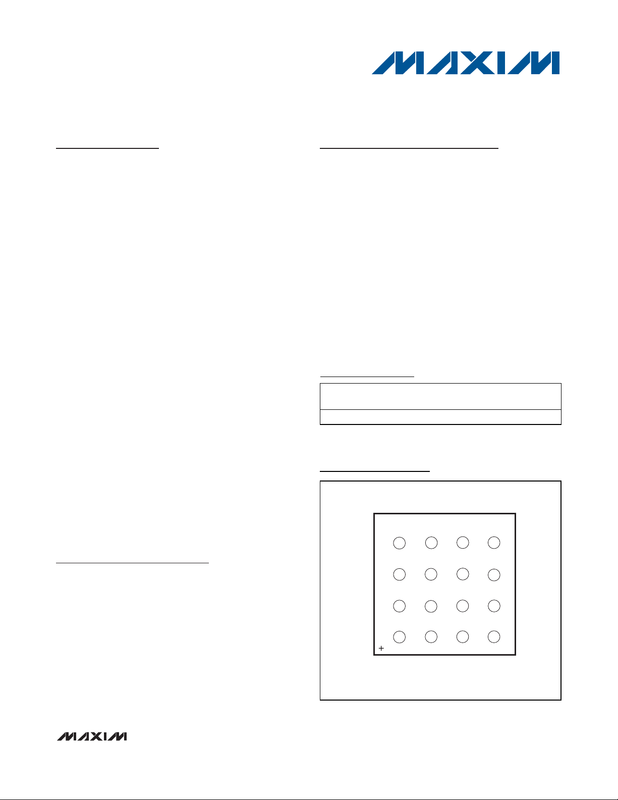
BOTTOM VIEW
MAX13000E/MAX13003E
I/OV
D
I/OV
C
I/OVL1 I/OVL5 I/OVL6
B
I/OV
A
V
3
CC
1 I/OVCC2
CC
I/OVL2
3VLEN I/OVL4
L
1
4 X 4 UCSP
GND
CC
I/OVCC5
234
I/OV
I/OV
CC
CC
PINPACKAGE
4
6
Page 2
MAX13000E–MAX13005E
Ultra-Low-Voltage Level Translators
2 _______________________________________________________________________________________
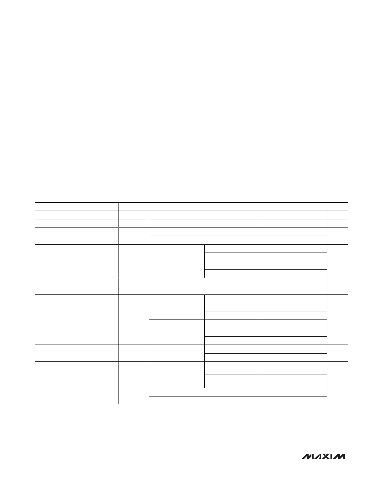
ABSOLUTE MAXIMUM RATINGS
ELECTRICAL CHARACTERISTICS
(VCC= +1.5V to +3.6V, VL= +0.9V to VCC, C
I/OVL
≤ 15pF, C
I/OVCC
≤ 50pF, TA= -40°C to +85°C, unless otherwise noted. Typical val-
ues are at T
A
= +25°C.) (Notes 1, 4)
Stresses beyond those listed under “Absolute Maximum Ratings” may cause permanent damage to the device. These are stress ratings only, and functional
operation of the device at these or any other conditions beyond those indicated in the operational sections of the specifications is not implied. Exposure to
absolute maximum rating conditions for extended periods may affect device reliability.
Voltages referenced to GND.
V
CC
...........................................................................-0.3V to +4V
V
L
..............................................................................-0.3V to +4V
I/O
VCC_
.......................................................-0.3V to (VCC+ 0.3V)
I/O
VL_
............................................................-0.3V to (VL+ 0.3V)
EN .................................................................-0.3V to (V
L
+ 0.3V)
Short-Circuit Duration I/O
VL_
, I/O
VCC_
to GND ..........Continuous
Continuous Power Dissipation (T
A
= +70°C)
16-Pin TSSOP (derate 9.4mW/°C at +70°C) ................755mW
16-Bump UCSP (derate 8.2mW/°C at +70°C) .............659mW
Operating Temperature Range ..........................-40°C to +85°C
Junction Temperature......................................................+150°C
Storage Temperature Range .............................-65°C to +150°C
Lead Temperature (soldering, 10s) .................................+300°C
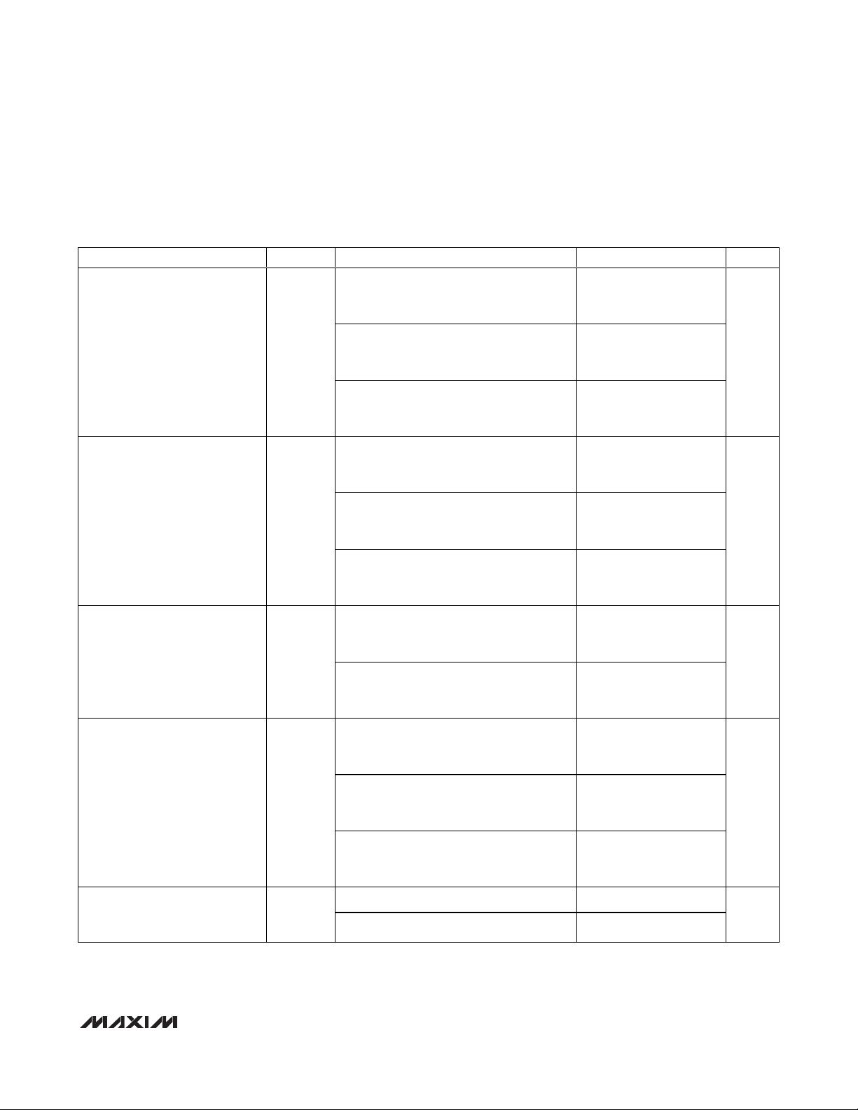
PARAMETER SYMBOL CONDITIONS MIN TYP MAX UNITS
VL Supply Range V
VCC Supply Range V
Supply Current from V
CC
(Note 3)
CC
I
QVCC
Supply Current from VL (Note 3) I
VCC Shutdown Supply Current
(Note 3)
VL Shutdown Supply Current
(Note 3)
I/O Tri-State Output Leakage
Current
I/O Tri-Stated Output Leakage
Current
EN Input Leakage Current
QVL
I
SHDN-VCC
L
VL ≤ V
CC
(Note 2) 0.9 V
(Note 2) 1.5 3.6 V
TA = +25°C4
TA = +85°C40
TA = +25°C
TA = +85°C
(Note 3) 1 5
< VCC - 0.2V 2
V
L
(Note 3) 4 40
< VCC - 0.2V 20
V
L
EN = GND, TA = +25°C2
EN = GND, TA = +85°C20
VL < VCC - 0.2V,
TA = +25°C
EN = GND
EN = GND 1 4
VL < VCC - 0.2V,
T
= +85°C
A
EN = GND
EN = GND 40
I/O V
, I/O V
L_
EN = GND
< VCC - 0.2V, I/O
V
L
, I/O V
V
L_
CC_
EN = GND
CC_
,
TA = +25°C 0.35
,
T
= +85°C1
A
TA = +25°C 0.2
T
= +85°C 0.5
A
TA = +25°C 0.35
= +85°C1
T
A
CC
2
20
V
µA
µA
µA
µA
µA
µA
µA
Page 3
MAX13000E–MAX13005E
Ultra-Low-Voltage Level Translators
_______________________________________________________________________________________ 3
ELECTRICAL CHARACTERISTICS (continued)
(VCC= +1.5V to +3.6V, VL= +0.9V to VCC, C
I/OVL
≤ 15pF, C
I/OVCC
≤ 50pF, TA= -40°C to +85°C, unless otherwise noted. Typical val-
ues are at T
A
= +25°C.) (Notes 1, 4)
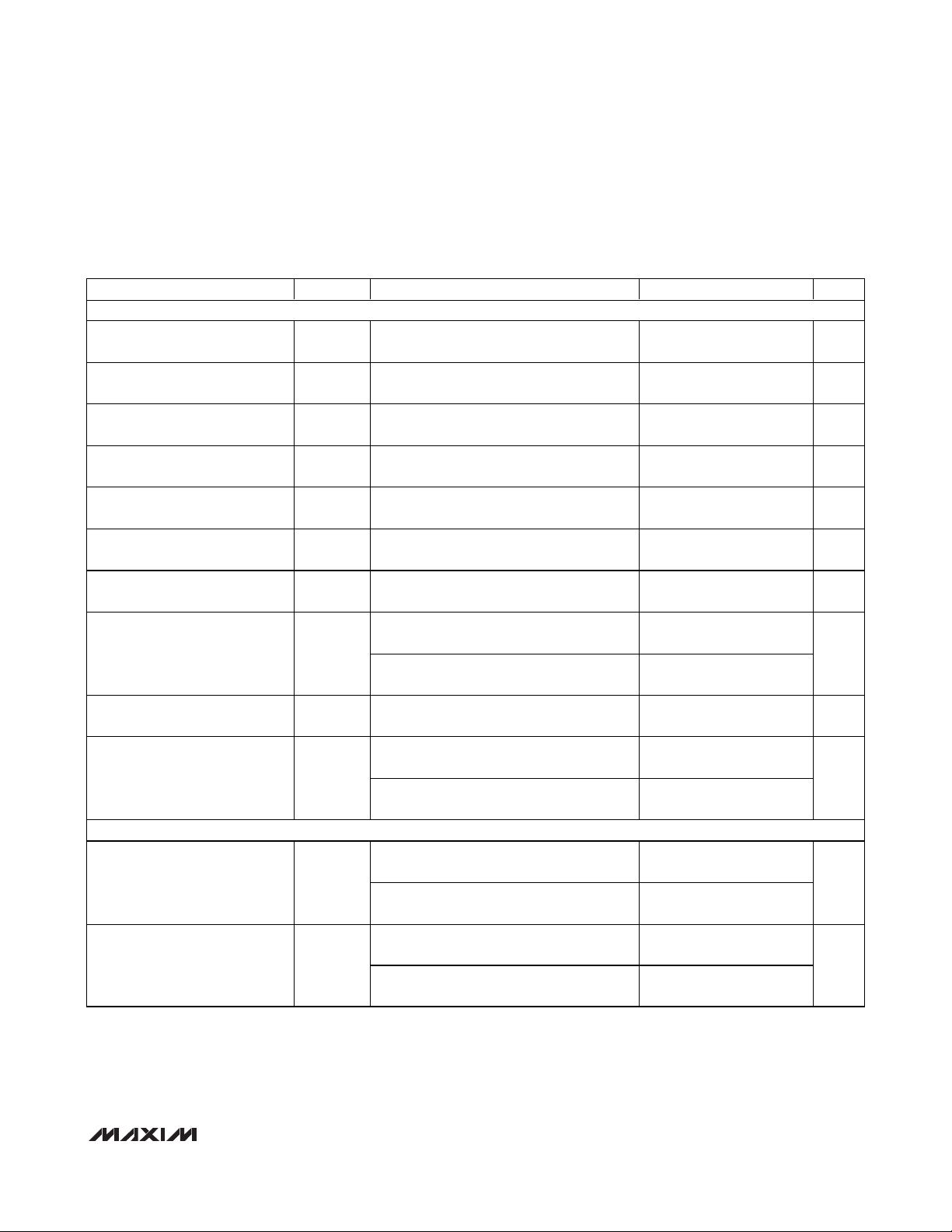
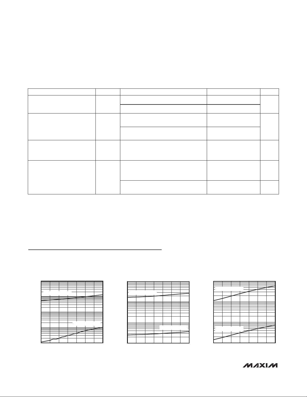
PARAMETER SYMBOL CONDITIONS MIN TYP MAX UNITS
LOGIC-LEVEL THRESHOLDS
I/OVL_ Input-Voltage-High
Threshold
I/OVL_ Input-Voltage-Low
Threshold
I/OV
Input-Voltage-High
CC_
Threshold
I/OV
Input-Voltage-Low
CC_
Threshold
EN Input-Voltage-High Threshold V
EN Input-Voltage-Low Threshold V
Output-Voltage High V
I/OV
L_
Output-Voltage Low V
I/OV
L_
I/OV
I/OV
Output-Voltage High V
CC_
Output-Voltage Low V
CC_
V
V
V
IHC
V
ILC
IHEN
ILEN
OHL
OLL
OHC
OLC
IHL
ILL
OUTPUT CURRENTS
Output Sink Current During
Transient (V
CC
Side)
Output Sink Current During
Transient (V
Side)
L
source current = 20µA
I/OV
L_
MAX13002E/MAX13005E,
OV
sink current = 1µA
L_
MAX13000E/MAX13001E/MAX13003E/
MAX13004E, I/OV
I/OV
source current = 20µA
CC_
L_
MAX13001E/MAX13004E,
sink current = 1µA
OV
CC_
MAX13000E/MAX13002E/MAX13003E/
MAX13005E, I/OV
CC_
VCC = +1.65V,
MAX13003E/MAX13004E/MAX13005E
V
= +1.65V,
CC
MAX13000E/MAX13001E/MAX13002E
VL = +1.2V, VCC = +1.65V,
MAX13003E/MAX13004E/MAX13005E
V
= +1.2V, VCC = +1.65V,
L
MAX13000E/MAX13001E/MAX13002E
sink current = 20µA
sink current = 20µA
1/3 × V
1/3 ×
V
CC
1/3 × V
V
-
L
0.25
V
CC
0.25
2/3 × V
L
2/3 ×
V
CC
2/3 × V
L
0.3
0.25
-
0.3
0.25
25
1
30
1
V
L
V
V
V
V
L
V
V
V
V
V
mA
mA
Page 4
MAX13000E–MAX13005E
Ultra-Low-Voltage Level Translators
4 _______________________________________________________________________________________
ELECTRICAL CHARACTERISTICS (continued)
(VCC= +1.5V to +3.6V, VL= +0.9V to VCC, C
I/OVL
≤ 15pF, C
I/OVCC
≤ 50pF, TA= -40°C to +85°C, unless otherwise noted. Typical val-
ues are at T
A
= +25°C.) (Notes 1, 4)
TIMING CHARACTERISTICS
(VCC= +1.5V to +3.6V, VL= +0.9V to VCC, C
I/OVL
≤ 15pF, C
I/OVCC
≤ 50pF, TA= -40°C to +85°C, unless otherwise noted. Typical val-
ues are at T
A
= +25°C.) (Notes 1, 4)
Output Source Current During
Transient (V
Output Source Current During
Transient (V
ESD PROTECTION
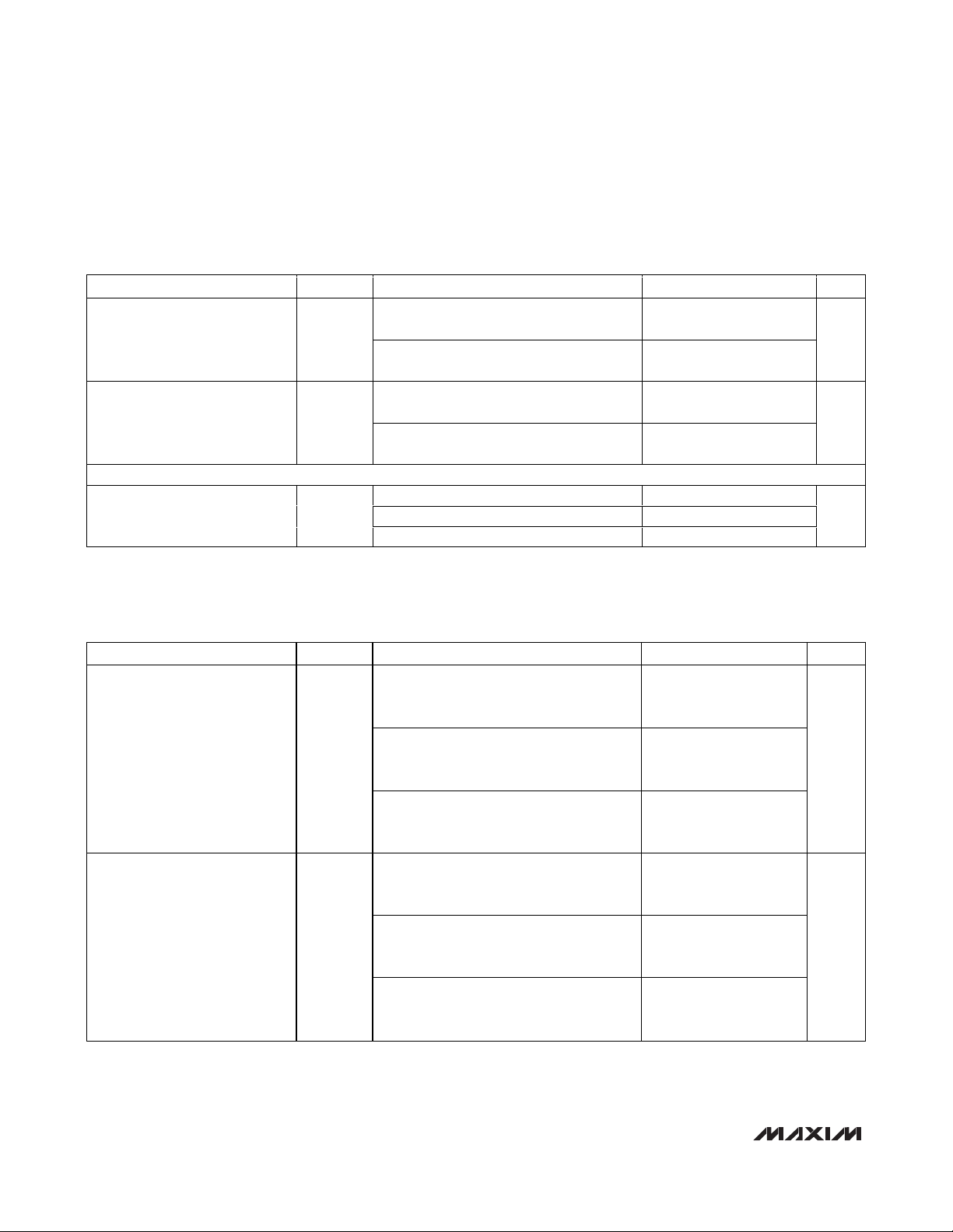
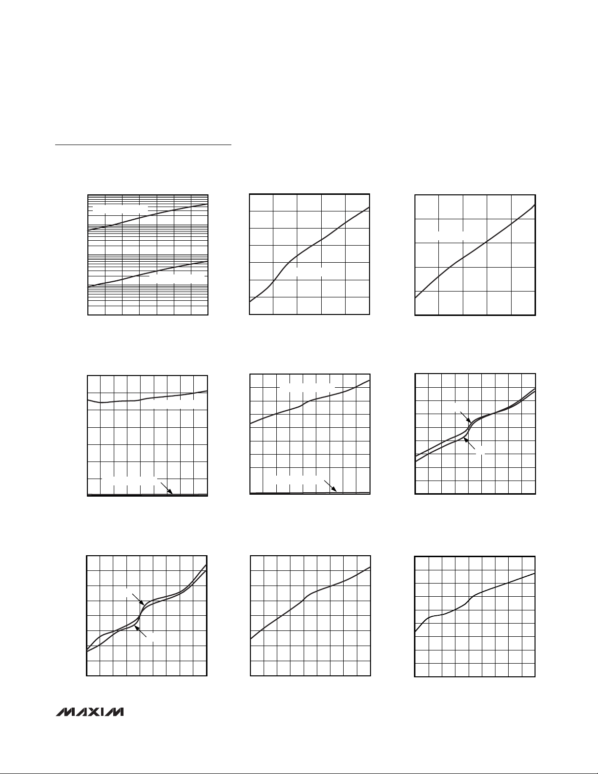
PARAMETER SYMBOL CONDITIONS MIN TYP MAX UNITS
Side)
CC
Side)
L
CC_
PARAMETER SYMBOL CONDITIONS MIN TYP MAX UNITS
VCC = +1.65V,
MAX13003E/MAX13004E/MAX13005E
V
= +1.65V,
CC
MAX13000E/MAX13001E/MAX13002E
VL = +1.2V, VCC = +1.65V,
MAX13003E/MAX13004E/MAX13005E
V
= +1.2V, VCC = +1.65V,
L
MAX13000E/MAX13001E/MAX13002E
Human Body Model ±15
Air-Gap Discharge (IEC61000-4-2) ±10I/OV
Contact Discharge (IEC61000-4-2) ±8
C
MAX13003E/MAX13004E/MAX13005E,
V
= 50pF,
I/OVCC
= +1.65V, Figures 1a, 1b
CC
22
mA
1
25
mA
1
kV
15
I/OV
Rise Time t
CC_
I/OV
Fall Time t
CC_
RVCC
FVCC
C
MAX13003E/MAX13004E/MAX13005E,
V
C
MAX13000E/MAX13001E/MAX13002E,
Figures 1a, 1b
C
MAX13003E/MAX13004E/MAX13005E,
V
C
MAX13003E/MAX13004E/MAX13005E,
V
C
MAX13000E/MAX13001E/MAX13002E,
Figures 1a, 1b
= 50pF,
I/OVCC
= +1.5V, Figures 1a, 1b
CC
= 50pF,
I/OVCC
= 50pF,
I/OVCC
= +1.65V, Figures 1a, 1b
CC
= 50pF,
I/OVCC
= +1.5V, Figures 1a, 1b
CC
= 50pF,
I/OVCC
400 1400
400 1400
15
15
15
ns
ns
Page 5
MAX13000E–MAX13005E
Ultra-Low-Voltage Level Translators
_______________________________________________________________________________________ 5
TIMING CHARACTERISTICS (continued)
(VCC= +1.5V to +3.6V, VL= +0.9V to VCC, C
I/OVL
≤ 15pF, C
I/OVCC
≤ 50pF, TA= -40°C to +85°C, unless otherwise noted. Typical val-
ues are at T
A
= +25°C.) (Notes 1, 4)
PARAMETER SYMBOL CONDITIONS MIN TYP MAX UNITS
I/OVL_ Rise Time t
I/OVL_ Fall Time t
RVL
FVL
C
= 50pF,
I/OVL
MAX13003E/MAX13004E/MAX13005E,
V
= +1.65V, Figures 2a, 2b
CC
C
= 15pF,
I/OVL
MAX13003E/MAX13004E/MAX13005E,
= +1.5V, Figures 2a, 2b
V
CC
C
= 50pF,
I/OVL
MAX13000E/MAX13001E/MAX13002E,
Figures 2a, 2b
C
= 50pF,
I/OVL
MAX13003E/MAX13004E/MAX13005E,
V
= +1.65V, Figures 2a, 2b
CC
C
= 15pF,
I/OVL
MAX13003E/MAX13004E/MAX13005E,
V
= +1.5V, Figures 2a, 2b
CC
C
= 50pF,
I/OVL
MAX13000E/MAX13001E/MAX13002E,
Figures 2a, 2b
300 1200
300 1200
15
15
15
15
ns
ns
Propagation Delay
(Driving I/OV
)
L_
Propagation Delay
(Driving I/OV
CC_
)
Propagation Delay from
I/OV
to I/OV
L
CC_
after EN
(Note 5)
I/O
VL-VCC
I/O
VCC-VL
t
EN-VCC
C
I/OVCC
= 50pF,
MAX13003E/MAX13004E/MAX13005E,
Figures 1a, 1b
C
I/OVCC
= 50pF,
MAX13000E/MAX13001E/MAX13002E,
Figures 1a, 1b
VCC > +1.65V, C
I/OVL
= 50pF,
MAX13003E/MAX13004E/MAX13005E,
Figures 2a, 2b
VCC = 1.5V, C
I/OVL
= 15pF,
MAX13003E/MAX13004E/MAX13005E,
Figures 2a, 2b
C
= 50pF,
I/OVL
MAX13000E/MAX13001E/MAX13002E,
Figures 2a, 2b
C
C
= 50pF, CMOS output, Figure 3 2
I/OVCC
= 50pF, OD output, Figure 3 6
I/OVCC
20
1000
20
20
1000
ns
ns
µs
Page 6
Typical Operating Characteristics
(VCC= +3.3V, VL= +0.9V, TA = +25°C, MAX13003E.)
0.1
1
10
100
1000
VL SUPPLY CURRENT vs. SUPPLY VOLTAGE
(DRIVING I/O V
L
, VL = 0.9V)
MAX13000Etoc01
SUPPLY VOLTAGE (V)
V
L
SUPPLY CURRENT (μA)
1.5 2.4 2.71.8 2.1 3.0 3.3 3.6
DATA RATE = 20Mbps
DATA RATE = 230kbps
VL SUPPLY CURRENT vs. SUPPLY VOLTAGE
(DRIVING I/O V
CC
, VL = 0.9V)
MAX13000Etoc02
SUPPLY VOLTAGE (V)
V
L
SUPPLY CURRENT (mA)
3.33.02.72.42.11.8
0.01
0.1
1
0.001
1.5 3.6
DATA RATE = 20Mbps
DATA RATE = 230kbps
VCC SUPPLY CURRENT vs. SUPPLY VOLTAGE
(DRIVING I/O V
L
, VL = 0.9V)
MAX13000Etoc03
SUPPLY VOLTAGE (V)
V
CC
SUPPLY CURRENT (mA)
3.33.02.72.42.11.8
0.1
1
10
0.01
1.5 3.6
DATA RATE = 230kbps
DATA RATE = 20Mbps
MAX13000E–MAX13005E
Ultra-Low-Voltage Level Translators
6 _______________________________________________________________________________________
TIMING CHARACTERISTICS (continued)
(VCC= +1.5V to +3.6V, VL= +0.9V to VCC, C
I/OVL
≤ 15pF, C
I/OVCC
≤ 50pF, TA= -40°C to +85°C, unless otherwise noted. Typical val-
ues are at T
A
= +25°C.) (Notes 1, 4)
Note 1: All devices are 100% production tested at TA= +25°C. Limits are guaranteed by design over the entire temperature range.
Note 2: V
L
must be less than or equal to VCCduring normal operation. However, VLcan be greater than VCCduring startup and
shutdown conditions.
Note 3: This consumption is referred to as no signal transmission.
Note 4: Guaranteed by design with an input signal full swing, rise/fall time ≤ 3ns, source resistance is 50Ω.
Note 5: Enable input signal full swing and rise/fall time ≤ 50ns.
Note 6: Guaranteed by design, not production tested.
PARAMETER SYMBOL CONDITIONS MIN TYP MAX UNITS
Propagation Delay from
I/OV
CC
to I/OVL after EN
t
EN-VL
(Note 5)
Channel-to-Channel Skew t
Part-to-Part Skew (Note 6) t
SKEW
PPSKEW
Maximum Data Rate
C
= 50pF, CMOS output, Figure 4 2
I/OVL
C
= 50pF, OD output, Figure 4 6
I/OVL
Each translator equally loaded,
MAX13003E/MAX13004E/MAX13005E
Each translator equally loaded,
MAX13000E/MAX13001E/MAX13002E
C
= 15pF, C
I/OVL
V
= +1.8V, VCC = +2V, ΔT = +5°C,
L
I/OVCC
= 15pF,
MAX13003E/MAX13004E/MAX13005E
MAX13003E/MAX13004E/MAX13005E
V
> +1.65V, C
CC
C
I/OVCC
= 50pF
I/OVL
= 50pF,
MAX13000E/MAX13001E/MAX13002E
C
I/OVL
= 50pF, C
I/OVCC
= 50pF
230 kbps
µs
±5
ns
±250
10 ns
20 Mbps
Page 7
MAX13000E–MAX13005E
Ultra-Low-Voltage Level Translators
_______________________________________________________________________________________ 7
Typical Operating Characteristics (continued)
(VCC= +3.3V, VL= +0.9V, TA = +25°C, MAX13003E.)
0.001
0.01
0.1
1.0
10
VCC SUPPLY CURRENT vs. SUPPLY VOLTAGE
(DRIVING I/OV
CC
, VL = +0.9V)
MAX13000Etoc04
SUPPLY VOLTAGE (V)
V
CC
SUPPLY CURRENT (mA)
1.5 2.4 2.71.8 2.1 3.0 3.3 3.6
DATA RATE = 230kbps
DATA RATE = 20Mbps
VL SUPPLY CURRENT vs. TEMPERATURE
(DRIVING I/OV
CC
, VCC = +3.3V, VL = +0.9V)
MAX13000E toc05
TEMPERATURE (°C)
V
CC
SUPPLY CURRENT (μA)
603510-15
300
310
320
330
340
290
-40 85
DATA RATE = 20Mbps
VCC SUPPLY CURRENT vs. TEMPERATURE
(DRIVING I/OV
CC
, VCC = +3.3V, VL = +0.9V)
MAX13000E toc06
TEMPERATURE (°C)
V
CC
SUPPLY CURRENT (mA)
603510-15
3.90
3.95
4.00
4.05
4.10
3.85
-40 85
DATA RATE = 20Mbps
0
40
20
80
60
120
100
140
10 30 4020 50 60 70 80 90 100
VL SUPPLY CURRENT vs.
CAPACITIVE LOAD ON I/O V
CC
(DRIVING I/OVL, VCC = 3.3V, VL = +0.9V)
MAX31000Etoc07
CAPACITIVE LOAD (pF)
V
L
SUPPLY CURRENT (μA)
DATA RATE = 20Mbps
DATA RATE = 230kbps
0
2
1
4
3
7
5
8
6
9
10 30 4020 50 60 70 80 90 100
VCC SUPPLY CURRENT vs.
CAPACITIVE LOAD ON I/O V
CC
(DRIVING I/OVL, VCC = 3.3V, VL = +0.9V)
MAX31000Etoc08
CAPACITIVE LOAD (pF)
V
CC
SUPPLY CURRENT (mA)
DATA RATE = 20Mbps
DATA RATE = 230kbps
0
2
1
4
3
7
5
8
6
9
10 30 4020 50 60 70 80 90 100
RISE/FALL TIME vs.
CAPACITIVE LOAD ON I/O V
CC
(DRIVING I/OVL, VCC = 3.3V, VL = +0.9V)
MAX31000Etoc09
CAPACITIVE LOAD (pF)
RISE/FALL TIME (ns)
t
F
t
R
0
2
1
4
3
7
5
6
8
10 30 4020 50 60 70 80 90 100
RISE/FALL TIME vs.
CAPACITIVE LOAD ON I/O V
L
(DRIVING I/OV
CC
, = 3.3V, VL = +0.9V)
MAX31000Etoc10
CAPACITIVE LOAD (pF)
RISE/FALL TIME (ns)
t
F
t
R
5.0
6.0
5.5
7.0
6.5
8.5
7.5
8.0
9.0
10 30 4020 50 60 70 80 90 100
PROPAGATION DELAY vs.
CAPACITIVE LOAD ON I/O V
CC
(DRIVING I/OV
L
, VCC, = 3.3V, VL = +0.9V)
MAX31000Etoc11
CAPACITIVE LOAD (pF)
PROPAGATION DELAY (ns)
2.0
3.0
2.5
4.5
4.0
3.5
5.5
6.0
5.0
6.5
10 40 5020 30 60 70 80 90 100
PROPAGATION DELAY vs.
CAPACITIVE LOAD ON I/O V
L
(DRIVING I/OV
CC
, VCC = 3.3V, VL = +0.9V)
MAX13000Etoc12
CAPACITIVE LOAD (pF)
PROPAGATION DELAY (ns)
Page 8
MAX13000E–MAX13005E
Ultra-Low-Voltage Level Translators
8 _______________________________________________________________________________________
Typical Operating Characteristics (continued)
(VCC= +3.3V, VL= +0.9V, TA = +25°C, MAX13003E.)
OD RAIL-TO-RAIL DRIVING (MAX13005E)
(DRIVING I/OV
= +0.9V, C
V
L
DATA RATE = 230Mbps, R
, VCC = +3.3V,
L
= 56pF,
I/OVCC
PULLUP
= 1kΩ)
OD RAIL-TO-RAIL DRIVING (MAX13002E)
(DRIVING I/OV
= +0.9V, C
V
L
DATA RATE = 230kbps, R
, VCC = +3.3V,
L
= 56pF,
I/OVCC
PULLUP
= 15kΩ)
(DRIVING I/OV
RAIL-TO-RAIL DRIVING
, VCC = +3.3V, VL = +0.9V,
L
= 50pF, DATA RATE = 230kbps)
C
I/OVCC
MAX31000Etoc13
I/OV
L_
500mV/div
GND
I/OV
CC
2V/div
GND
200ns/div
RAIL-TO-RAIL DRIVING
(DRIVING I/OV
C
I/OVCC
L VCC
= 50pF, DATA RATE = 4Mbps)
= +3.3V, VL = +0.9V,
(DRIVING I/OV
RAIL-TO-RAIL DRIVING
= 50pF, DATA RATE = 20Mbps)
C
I/OVCC
2μs/div
, VCC = +3.3V, VL = +0.9V,
L
MAX31000Etoc16
I/OV
L_
500mV/div
GND
I/OV
CC
2V/div
GND
40ns/div
VCC + VL SUPPLY CURRENT vs. FREQUENCY
(DRIVING I/OV
13
I/OV
12
3.3V SQUARE WAVE
11
10
9
8
7
6
5
SUPPLY CURRENT (mA)
L
4
+ V
3
CC
V
2
1
0
100 84004250 12,550 16,700 20,850 25,000
, VCC = +3.3V, VL = +0.9V)
CC
IS DRIVEN WITH A
CC
VCC + V
FREQUENCY (kHz)
L
V
CC
V
L
MAX31000Etoc19
(V)
V
OHL
3.0
2.5
2.0
1.5
1.0
0.5
0
10ns/div
V
vs. I
OHL
020155 10 253035404550
OHL
= 3.3V)
(V
CC
VL = +2.5V
VL = +1.8V
VL = +0.9V
I
(μA)
OHL
FOR VL SIDE
MAX31000Etoc14
I/OV
500mV/div
GND
I/OV
2V/div
GND
MAX31000Etoc17
I/OV
L_
500mV/div
GND
I/OV
CC
2V/div
GND
L_
CC
SUPPLY CURRENT (mA)
L
+ V
CC
V
0.25
0.20
MAX13000Etoc20
0.15
(V)
OLL
V
0.10
0.05
1μs/div
VCC + VL SUPPLY CURRENT vs. FREQUENCY
(DRIVING I/OV
13
I/OVL IS DRIVEN WITH A
12
0.9V SQUARE WAVE
11
10
9
8
7
6
5
4
3
2
1
0
100 84004250 12,550 16,700 20,850 25,000
0
020155 10 253035404550
, VCC = +3.3V, VL = +0.9V)
L
VCC + V
L
FREQUENCY (kHz)
V
vs. I
(V
OLL
= 3.3V)
CC
I
OLL
FOR VL SIDE
(μA)
OLL
VL = +2.5V
VL = +1.8V
VL = +0.9V
V
CC
V
L
MAX31000Etoc15
I/OV
L_
500mV/div
GND
I/OV
CC
2V/div
GND
MAX31000Etoc18
MAX13000Etoc21
Page 9

MAX13000E–MAX13005E
Ultra-Low-Voltage Level Translators
_______________________________________________________________________________________ 9
Pin Descriptions
MAX13000E/MAX13003E
0
0.15
0.10
0.05
0.20
0.25
020155 10 253035404550
V
OLC
vs.
I
OLC
FOR VCC SIDE
MAX13000Etoc22
I
OLC
(μA)
V
OLC
(V)
VCC = +2.5V
VCC = +1.8V
VCC = +3.3V
1.0
2.5
2.0
1.5
3.0
3.5
020155 10 253035404550
V
OHC
vs.
I
OHC
FOR VCC SIDE
MAX13000Etoc23
I
OHC
(μA)
V
OHC
(V)
VCC = +3.3V
VCC = +1.8V
VCC = +2.5V
Typical Operating Characteristics (continued)
(VCC= +3.3V, VL= +0.9V, TA = +25°C, MAX13003E.)
PIN
TSSOP UCSP
1 B1 I/OVL1 CMOS Input/Output 1, Referenced to V
2 B2 I/OVL2 CMOS Input/Output 2, Referenced to V
3 A1 I/OVL3 CMOS Input/Output 3, Referenced to V
4A2 V
5A3 EN
6 A4 I/OVL4 CMOS Input/Output 4, Referenced to V
7 B3 I/OVL5 CMOS Input/Output 5, Referenced to V
8 B4 I/OVL6 CMOS Input/Output 6, Referenced to V
9 C4 I/OVCC6 CMOS Input/Output 6, Referenced to V
10 C3 I/OVCC5 CMOS Input/Output 5, Referenced to V
11 D4 I/OVCC4 CMOS Input/Output 4, Referenced to V
12 D3 GND Ground
13 D2 V
14 D1 I/OVCC3 CMOS Input/Output 3, Referenced to V
15 C2 I/OVCC2 CMOS Input/Output 2, Referenced to V
16 C1 I/OVCC1 CMOS Input/Output 1, Referenced to V
NAME FUNCTION
L
Logic Input Voltage, +0.9V ≤ VL ≤ VCC. Bypass VL to GND with a 0.1µF
capacitor.
Enable Input. When EN is pulled low, I/O V
6 are tri-stated. Drive EN high (VL) for normal operation.
V
L
CC
VCC Input Voltage, +1.5V ≤ VCC ≤ 3.6V. Bypass VCC to GND with a 0.1µF
capacitor. For full ESD protection, use a 1µF bypass capacitor on V
L
L
L
1 to I/O VCC6 and I/O VL1 to I/O
CC
L
L
L
CC
CC
CC
CC
CC
CC
CC
.
Page 10

MAX13000E–MAX13005E
Ultra-Low-Voltage Level Translators
10 ______________________________________________________________________________________
MAX13001E/MAX13004E
Pin Descriptions (continued)
PIN
TSSOP UCSP
1B1OV
2B2OV
3A1OV
4A2 V
5A3 EN
6A4OV
7B3OV
8B4OV
9C4IV
10 C3 IVCC5 Open-Drain-Compatible Input 5, Referenced to V
11 D4 IVCC4 Open-Drain-Compatible Input 4, Referenced to V
12 D3 GND Ground
13 D2 V
14 D1 IVCC3 Open-Drain-Compatible Input 3, Referenced to V
15 C2 IVCC2 Open-Drain-Compatible Input 2, Referenced to V
16 C1 IVCC1 Open-Drain-Compatible Input 1, Referenced to V
NAME FUNCTION
1 CMOS Output 1, Referenced to V
L
2 CMOS Output 2, Referenced to V
L
3 CMOS Output 3, Referenced to V
L
L
4 CMOS Output 4, Referenced to V
L
5 CMOS Output 5, Referenced to V
L
6 CMOS Output 6, Referenced to V
L
6 Open-Drain-Compatible Input 6, Reference to V
CC
CC
Logic Input Voltage, +0.9V ≤ VL ≤ VCC. Bypass VL to GND with a 0.1µF
capacitor.
Enable Input. When EN is pulled low, OV
tri-stated. Drive EN high (V
VCC Input Voltage, +1.5V ≤ VCC ≤ 3.6V. Bypass VCC to GND with a 0.1µF
capacitor. For full ESD protection, use a 1µF bypass capacitor on V
L
L
L
) for normal operation.
L
L
L
L
1 to OVCC6 and IVL1 to IVL6 are
CC
CC
CC
CC
CC
CC
CC
CC
.
Page 11

MAX13000E–MAX13005E
Ultra-Low-Voltage Level Translators
______________________________________________________________________________________ 11
MAX13002E/MAX13005E
Pin Descriptions (continued)
PIN
TSSOP UCSP
1B1 IV
2B2 IV
3A1 IV
4A2 V
5A3 EN
6A4 IV
7B3 IV
8B4 IV
9C4OV
10 C3 OVCC5 CMOS Output 5, Referenced to V
11 D4 OVCC4 CMOS Output 4, Referenced to V
12 D3 GND Ground
13 D2 V
14 D1 OVCC3 CMOS Output 3, Referenced to V
15 C2 OVCC2 CMOS Output 2, Referenced to V
16 C1 OVCC1 CMOS Output 1, Referenced to V
NAME FUNCTION
1 Open-Drain-Compatible Input 1, Referenced to V
L
2 Open-Drain-Compatible Input 2, Referenced to V
L
3 Open-Drain-Compatible Input 3, Referenced to V
L
L
4 Open-Drain-Compatible Input 4, Referenced to V
L
5 Open-Drain-Compatible Input 5, Referenced to V
L
6 Open-Drain-Compatible Input 6, Referenced to V
L
6 CMOS Output 6, Referenced to V
CC
CC
Logic Input Voltage, +0.9V ≤ VL ≤ VCC. Bypass VL to GND with a 0.1µF
capacitor.
Enable Input. When EN is pulled low, OV
tri-stated. Drive EN high (V
VCC Input Voltage, +1.5V ≤ VCC ≤ 3.6V. Bypass VCC to GND with a 0.1µF
capacitor. For full ESD protection, use a 1µF bypass capacitor on V
L
L
L
1 to OVCC6 and IVL1 to IVL6 are
CC
CC
CC
CC
CC
CC
CC
L
L
L
.
CC
) for normal operation.
L
Page 12

MAX13000E–MAX13005E
Ultra-Low-Voltage Level Translators
12 ______________________________________________________________________________________
Test Circuits/Timing Diagrams
Figure 1a. Driving I/OVL
Figure 1b. Timing for Driving I/OV
L
Figure 2a. Driving I/OV
CC
Figure 2b. Timing for Driving I/OV
CC
I/OV
L_
90%
V
L
SOURCE
MAX13000E
EN
I/OV
L_
R
S
UNUSED I/Os ARE GROUNDED.
I/OV
CC
C
I/OVCC
V
CC
I/OV
t
t
50%
10%
t
RISE/FALL
CC_
RISE/FALL
RISE/FALL
90%
50%
t
FVCC
I/O
VL-VCC
< 3ns (MAX13003E/MAX13004E/MAX13005E)
< 80ns (MAX13000E/MAX13001E/MAX13002E)
10%
I/O
VL-VCC
t
RVCC
V
L
I/OV
L_
C
I/OVL
MAX13000E
EN
UNUSED I/Os ARE GROUNDED.
I/OV
R
SOURCE
V
CC
CC
S
t
I/OV
I/OV
CC_
L_
RISE/FALL
90%
50%
10%
I/O
VCC-VL
90%
50%
10%
t
FVL
t
< 3ns (MAX13003E/MAX13004E/MAX13005E)
RISE/FALL
< 80ns (MAX13000E/MAX13001E/MAX13002E)
t
RISE/FALL
I/O
VCC-VL
t
RVL
Page 13

MAX13000E–MAX13005E
Ultra-Low-Voltage Level Translators
______________________________________________________________________________________ 13
Test Circuits/Timing Diagrams (continued)
Figure 3. Propagation Delay from I/OVLto I/OVCCAfter EN
Figure 4. Propagation Delay from I/OVCCto I/OVLAfter EN
MAX13000E
SOURCE
V
SOURCE
V
SOURCE
L
I/OV
C
I/OVL
EN
I/OV
I/OV
I/OV
CC
I/OV
L_
L
MAX13000E
EN
I/OV
L_
MAX13000E
EN
L_
V
AND t"
L
0
V
L
0
V
CC
0
V
L
0
V
L
0
V
CC
0
EN-VCC
.
EN
CC
C
I/OVCC
I/OV
I/OV
L_
CC_
t'
EN-VCC
t"
EN-VCC
V
/ 2
CC
EN
I/OV
L_
CC
I/OV
I/OV
CC_
CC_
t
EN-VCC
EN
V
/ 2
CC
IS WHICH EVER IS LARGER BETWEEN t'
t'
EN-VL
EN-VCC
V
0
V
L
CC
C
I/OVCC
0
V
V
CC
I/OV
L_
VL / 2
L
0
SOURCE
L
I/OV
L_
C
I/OVL
EN
MAX13000E
I/OV
CC
V
EN
I/OV
CC_
I/OV
L_
t
IS WHICH EVER IS LARGER BETWEEN t'
EN-VL
t"
EN-VL
VL / 2
EN-VL
AND t"
V
L
0
V
CC
0
V
L
0
EN-VL
.
Page 14

MAX13000E–MAX13005E
Detailed Description
The MAX13000E–MAX13005E logic-level translators
provide the level shifting necessary to allow data transfer in multivoltage systems. Externally applied voltages,
VCCand VL, set the logic levels on each side of the
device. Logic signals present on the VLside of the
device appear as higher voltage logic signals on the
VCCside of the device, and vice-versa.
The MAX13000E/MAX13003E are bidirectional level
translators allowing data translation in either direction
(V
L
↔ VCC) on any single data line without the use of a
DIRECTION input. The MAX13001E/MAX13002E/
MAX13004E/MAX13005E unidirectional level translators
level shift data in one direction (V
L
→ VCCor VCC→
V
L
) on any single data line. The MAX13001E/
MAX13002E/MAX13004E/MAX13005E unidirectional
translators’ inputs have the capability to interface with
both CMOS and open-drain (OD) outputs. For more
information, see the Ordering Information section and
the Input Driver Requirements section.
The MAX13000E–MAX13005E accept V
L
from +0.9V to
+3.6V. All devices have V
CC
ranging from +1.5V to
+3.6V, making them ideal for data transfer between
low-voltage ASICs/PLDs and higher voltage systems.
The MAX13000E–MAX13005E feature low VCCquiescent supply current of less than 4µA, and VLquiescent
supply current of less than 2µA when in shutdown. The
MAX13000E–MAX13005E have ±15kV ESD protection
on the V
CC
side for greater protection in applications
that route signals externally. The ESD protection is
specified using the Human Body Model (HBM).The
MAX13000E/MAX13001E/MAX13002E operate at a
guaranteed 230kbps data rate. The MAX13003E/
MAX13004E/MAX13005E operate at a guaranteed
20Mbps data rate when VCC> +1.65V.
Level Translation
For normal operation, ensure that +1.5V ≤ VCC≤ +3.6V,
and +0.9V ≤ VL≤ VCC. During power-up sequencing,
VL≥ VCCdoes not damage the device whenever VLis
within the absolute maximum ratings (see the Absolute
Maximum Ratings section). During power-supply
sequencing, when VCCis floating and VLis powered
up, 1mA of current can be sourced to each load on the
VLside, yet the device does not latch up.
The MAX13000E–MAX13005E are designed to have
VCC≥ VLat all times; however, if VCCis turned off, the
part will not be damaged and will not latch up. To prevent excessive leakage currents in either the I/O or
supply lines, the I/O on the VLside must be left in the
high state.
The maximum data rate for the MAX13000E–
MAX13005E depends heavily on the load capacitance
(see the Typical Operating Characteristics), output
impedance of the driver, and the operational voltage
range (see the Timing Characteristics table).
Open-Drain Operation
The MAX13001E/MAX13002E/MAX13004E/MAX13005E
have input stages specifically designed to accommodate external open-drain drivers. When using opendrain drivers, the MAX13001E/MAX13002E/
MAX13004E/MAX13005E operate in a unidirectionalonly mode, translating from the OD side to the CMOS
side. For improved performance, the rise- and fall-time
accelerators are present on both the CMOS and the
OD side. See the Input-Driver Requirement section. Do
not use pullup resistors greater than 15kΩ for proper
operation, and smaller pullup resistance may be needed for higher speed operation.
Input-Driver Requirements
The MAX13000E–MAX13005E feature four different
architectures based on the speed of the part, as well as
on whether the translator is a CMOS-to-CMOS translator, or whether it is an OD-to-CMOS translator.
20Mbps CMOS-to-CMOS Bidirectional Translator
(MAX13003E)
The MAX13003E architecture is based on a one-shot
accelerator output stage (Figure 5). Accelerator output
stages are always in tri-state, except when there is a
transition on any of the translators on the input side,
either I/OVLor I/OVCC. A short pulse is generated during which the one-shot output stage becomes active
and charges/discharges the capacitances at the I/Os.
Due to its bidirectional nature, the accelerator stages on
both the I/OVCCand the I/OVLbecome active during an
I/O transition from low to high or high to low. This can
lead to some current feeding into the external source
that is driving the translator. However, this behavior
helps speed up the transition on the driven side.
The type of devices that drive the inputs of the
MAX13003E is usually specified with an output drivecurrent capability (I
OUT
). When driving the inputs of the
MAX13003E, the maximum achievable speed is constrained by the drive current of the external driver. To
insure the maximum possible throughput of 20Mbps, the
external driver should meet the following requirement:
I
OUT
≥ 1.67 × 10⁸ × V × (CIN+ CP)
Ultra-Low-Voltage Level Translators
14 ______________________________________________________________________________________
Page 15

where, CPis the parasitic capacitance of the traces, V
is the supply voltage of the driven side (i.e., VLor VCC),
and CINis the input capacitance of the driven side
(CIN= 10pF for VLside, CIN= 20pF for VCCside).
20Mbps OD-to-CMOS Unidirectional Translators
(MAX13004E/MAX13005E)
The MAX13004E/MAX13005E architecture is virtually the
same as that for the bidirectional CMOS-to-CMOS translators, the only difference being that the output inverter
(inverter 4) at the driving side accommodates the driving
capabilities of an open-drain output (Figure 6).
For proper operation, a pullup resistor needs to be connected from the open-drain output to the power supply of
the driving side. Use pullup resistors no larger than 15kΩ.
230kbps CMOS-to-CMOS Bidirectional Translator
(MAX13000E)
The architecture of the MAX13000E lacks the one-shot
accelerator output stages since the transitions that this
device handles are limited by its data rate, 230kbps
(Figure 7).
For proper operation, the driver must meet the following
conditions: 1kΩ maximum output impedance and 1mA
minimum output current.
230kbps OD-to-CMOS Unidirectional Translators
(MAX13001E/MAX13002E)
The architecture of the MAX13001E/MAX13002E is similar to that of the 230kbps CMOS-to-CMOS part, with the
difference that it accommodates the driving capability of
an open-drain output on the driving side, and also that it
has only a single one-shot output stage (Figure 8).
For proper operation, a pullup resistor needs to be connected from the open-drain output to the power supply of
the driving side. Use pullup resistors no larger than 15kΩ.
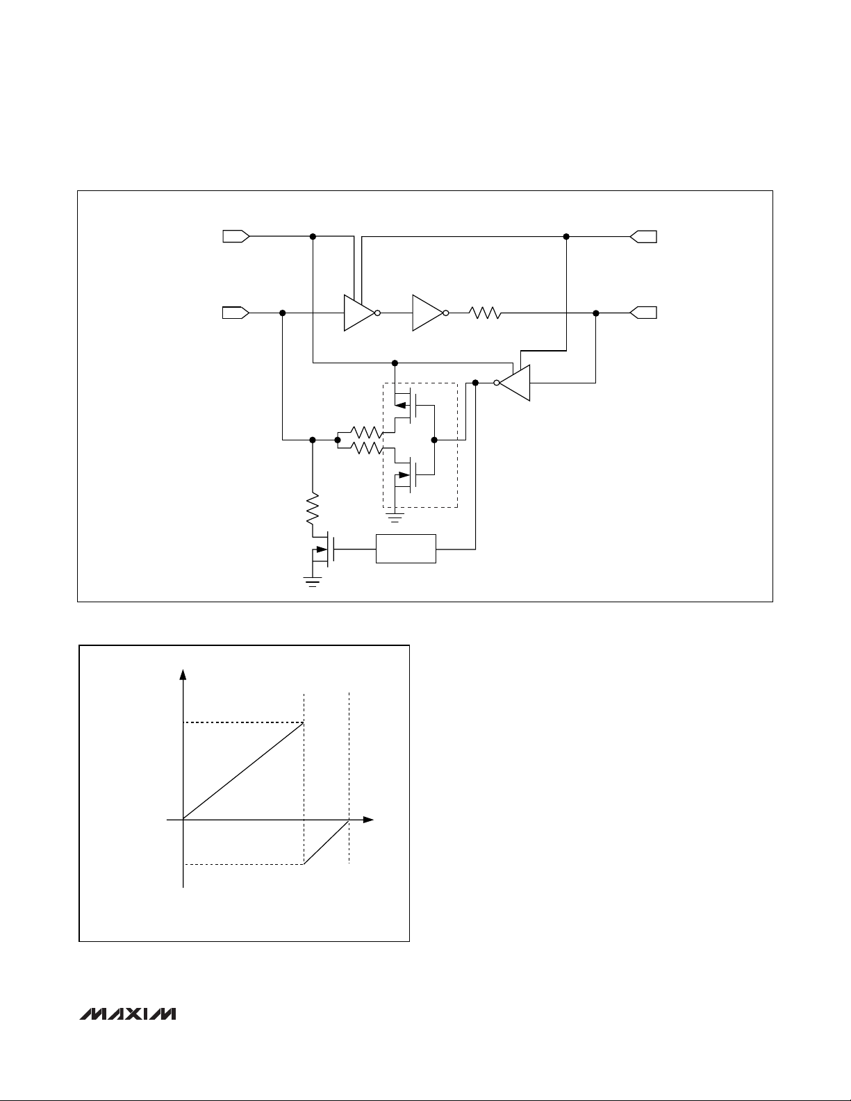
Figure 9 shows a graph of the typical input current versus input voltage for all of the above configurations.
Enable Output Mode (EN)
The MAX13000E–MAX13005E feature an enable (EN)
input. Drive EN low to set the MAX13000E–MAX13005E
I/Os in tri-state mode. Drive EN high (V
L
) for normal
operation.
±15kV ESD Protection
As with all Maxim devices, ESD-protection structures
are incorporated on all pins to protect against electrostatic discharges encountered during handling and
assembly. The I/OVCClines have extra protection
against static discharge. Maxim’s engineers have
developed state-of-the-art structures to protect these
pins against ESD of ±15kV without damage. The ESD
MAX13000E–MAX13005E
Ultra-Low-Voltage Level Translators
______________________________________________________________________________________ 15
I/OV
Figure 5. Architecture of 20Mbps, CMOS-to-CMOS Bidirectional Translators
V
L
P
ONE-SHOT
L
INVERTER 1
ONE-SHOT
P
ONE-SHOT
5kΩ
5kΩ
INVERTER 2
N
V
I/OV
CC
CC
INVERTER 4
N
ONE-SHOT
INVERTER 3
Page 16

MAX13000E–MAX13005E
Ultra-Low-Voltage Level Translators
16 ______________________________________________________________________________________
Figure 6. Architecture of 20Mbps, OD-to-CMOS Unidirectional Translators
Figure 7. Architecture of 230kbps, CMOS-to-CMOS Bidirectional Translator
20Mbps OPEN-DRAIN-TO-CMOS UNIDIRECTIONAL LEVEL TRANSLATOR
V
CC/VL
P
ONE-SHOT
IVCC/IV
L
OPEN-DRAIN
COMPATIBLE INPUT
INVERTER 1
INVERTER 2
ONE-SHOT
P
ONE-SHOT
5kΩ
N
V
L/VCC
OVL/OV
CMOS-
COMPATIBLE INPUT
CC
5kΩ
75kΩ
N
ONE-SHOT
230kbps Bidirectional CMOS-TO-CMOS Level Translator
V
L
I/OV
L
INVERTER 1
INVERTER 2
INVERTER
4
INVERTER 3
5kΩ
V
I/OV
CC
CC
5kΩ
INVERTER 4
INVERTER 3
Page 17
MAX13000E–MAX13005E
Ultra-Low-Voltage Level Translators
______________________________________________________________________________________ 17
structures withstand high ESD in all states: normal
operation, tri-state output mode, and power-down. After
an ESD event, Maxim’s E-versions keep working without latchup, whereas competing products can latch
and must be powered-down to remove latchup.
ESD protection can be tested in various ways. The
I/OVCClines of the MAX13000E–MAX13005E are characterized for protection to ±15kV using the Human
Body Model.
ESD Test Conditions
ESD performance depends on a variety of conditions.
Contact Maxim for a reliability report that documents
test setup, test methodology, and test results.
Human Body Model
Figure 10 shows the Human Body Model and Figure 11
shows the current waveform it generates when discharged into a low impedance. This model consists of
a 100pF capacitor charged to the ESD voltage of interest, which is then discharged into the test device
through a 1.5kΩ resistor.
V
Figure 8. Architecture of 230kbps, OD-to-CMOS Unidirectional Translator
Figure 9. Typical IINvs. V
IN
CC/VL
230kbps OPEN-DRAIN-TO-CMOS UNIDIRECTIONAL LEVEL TRANSLATOR
VL/V
CC
IVCC/IV
L
OPEN-DRAIN
COMPATIBLE INPUT
5kΩ
75kΩ
5kΩ
INVERTER 2INVERTER 1
INVERTER
4
N
ONE-SHOT
I
IN
V
TH_IN
/ R
IN1
0
(VS - V
) /
TH_IN
R
IN2
R
= R
= 5kΩ FOR CMOS-TO-CMOS TRANSLATORS
IN1
IN2
= 75kΩ FOR OD-TO-CMOS TRANSLATORS
R
IN1
V
TH_IN
WHERE, VS = VCC OR V
V
IN
V
S
L
5kΩ
INVERTER 3
OVL/OV
CC
CMOS-
COMPATIBLE INPUT
Page 18

MAX13000E–MAX13005E
IEC 61000-4-2 Standard ESD Protection
The IEC 61000-4-2 standard (Figure 12) specifies ESD
tolerance for electronic systems. The IEC61000-4-2
model specifies a 150pF capacitor that is discharged
into the device through a 330Ω resistor. The
MAX13000E–MAX13005E’s I/O on the VCCside are
rated for IEC 61000-4-2 standard, (8kV Contact
Discharge and ±10kV Air-Gap Discharge).
The IEC 61000-4-2 model discharges higher peak current and more energy than the HBM due to the lower
series resistance and larger capacitor.
Applications Information
Power-Supply Decoupling
To reduce ripple and the chance of transmitting incorrect data, bypass VLand VCCto ground with a 0.1µF
capacitor. To ensure full ±15kV ESD protection, bypass
VCCto ground with a 1µF capacitor. Place all capacitors as close to the power-supply inputs as possible.
UCSP Package Considerations
For general UCSP package information and PC layout
considerations, please refer to Maxim application note:
Wafer-Level Chip-Scale Package.
UCSP Reliability
The chip-scale package (UCSP) represents a unique
packaging form factor that may not perform equally to a
packaged product through traditional mechanical reliability tests. UCSP reliability is integrally linked to the
user’s assembly methods, circuit board material, and
usage environment. The user should closely review
these areas when considering use of a UCSP package.
Performance through Operating Life Test and Moisture
Resistance remains uncompromised as it is primarily
determined by the wafer-fabrication process.
Mechanical stress performance is a greater consideration for a UCSP package. UCSPs are attached through
direct solder contact to the user’s PC board, foregoing
the inherent stress relief of a packaged product lead
frame. Solder joint contact integrity must be considered. Information on Maxim’s qualification plan, test
data, and recommendations are detailed in the UCSP
application note, which can be found on Maxim’s website at www.maxim-ic.com.
Ultra-Low-Voltage Level Translators
18 ______________________________________________________________________________________
Figure 10. Human Body ESD Test Model
Figure 12. IEC 61000-4-2 Contact Discharge Test Model
Figure 11. Human Body Current Waveform
1MΩ RD 1500Ω
R
C
CHARGE-CURRENT-
LIMIT RESISTOR
HIGH-
VOLTAGE
DC
SOURCE
100pF
C
S
DISCHARGE
RESISTANCE
STORAGE
CAPACITOR
DEVICE
UNDER
TEST
I
100%
P
90%
AMPERES
36.8%
10%
0
0
t
RL
TIME
CURRENT WAVEFORM
I
r
t
DL
PEAK-TO-PEAK RINGING
(NOT DRAWN TO SCALE)
HIGH-
VOLTAGE
DC
SOURCE
R
C
50Ω TO 100Ω
CHARGE-CURRENT-
LIMIT RESISTOR
C
s
150pF
R
D
330Ω
DISCHARGE
RESISTANCE
STORAGE
CAPACITOR
DEVICE
UNDER
TEST
Page 19

MAX13000E–MAX13005E
Ultra-Low-Voltage Level Translators
______________________________________________________________________________________ 19
Functional Diagram
I/OV
I/OV
I/OV
V
L
EN
V
CC
MAX13000E–MAX13005E
1
L
2
L
3
L
I/OV
CC
I/OV
CC
I/OVCC3
1
2
I/OV
I/OVL5
I/OVL6
4
L
GND
I/OVCC4
I/OVCC5
I/OV
CC
6
Page 20

MAX13000E–MAX13005E
Ultra-Low-Voltage Level Translators
20 ______________________________________________________________________________________
Typical Operating Circuits
+0.9V
0.1μF1μF
+0.9V
SYSTEM
CONTROLLER
DATA1
DATA2
DATA3
DATA4
DATA5
DATA6
EN
OVL_1
OV
L_
OV
L_
OV
L_
OV
L_
OV
L_
V
MAX13001E
MAX13004E
2
3
4
5
6
V
L
CC
IV
IV
IV
IV
IV
IV
GND
+0.9V
CC_
CC_
CC_
CC_
CC_
CC_
+2.8V
+2.8V
SYSTEM
1
2
3
4
5
6
DATA1
DATA2
DATA3
DATA4
DATA5
DATA6
+2.8V
0.1μF1μF
+0.9V
SYSTEM
CONTROLLER
DATA1
DATA2
DATA3
DATA4
DATA5
DATA6
EN
IVL_1
IV
L_
IV
L_
IV
L_
IV
L_
IV
L_
V
MAX13002E
MAX13005E
2
3
4
5
6
V
L
GND
CC
1
OV
CC_
2
OV
CC_
3
OV
CC_
4
OV
CC_
OV
5
CC_
OV
6
CC_
+2.8V
SYSTEM
DATA1
DATA2
DATA3
DATA4
DATA5
DATA6
Page 21

MAX13000E–MAX13005E
Ultra-Low-Voltage Level Translators
______________________________________________________________________________________ 21
Typical Operating Circuits (continued)
Selector Guide
+0.9V
+0.9V
SYSTEM
CONTROLLER
DATA1
DATA2
DATA3
DATA4
DATA5
DATA6
0.1μF
+2.8V
1μF
EN
I/OVL_1
I/OV
L_
I/OV
L_
I/OV
L_
I/OV
L_
I/OV
L_
V
MAX13000E
MAX13003E
2
3
4
5
6
V
L
GND
CC
I/OV
I/OV
I/OV
I/OV
I/OV
I/OV
CC_
CC_
CC_
CC_
CC_
CC_
1
2
3
4
5
6
+2.8V
SYSTEM
DATA1
DATA2
DATA3
DATA4
DATA5
DATA6
NUMBER OF
V
→ V
CC
L
TRANSLATORS
TRANSLATOR
CONFIGURATION
PART
DATA
RATE
(bps)
NUMBER OF
BIDIRECTIONAL
TRANSLATORS
NUMBER OF
VL → V
CC
TRANSLATORS
MAX13000E 230k 6 — — CMOS-to-CMOS
MAX13001E 230k — — 6 OD-to-CMOS
MAX13002E 230k — 6 — OD-to-CMOS
MAX13003E 20M 6 — — CMOS-to-CMOS
MAX13004E 20M — — 6 OD-to-CMOS
MAX13005E 20M — 6 — OD-to-CMOS
Page 22

MAX13000E–MAX13005E
Ultra-Low-Voltage Level Translators
22 ______________________________________________________________________________________
Pin Configurations (continued)
BOTTOM VIEW
MAX13001E/MAX13004E MAX13002E/MAX13005E
V
3
IV
CC
D
IV
1IVCC2
CC
C
OVL1OV
B
OV
A
OVL2
3VLEN OVL4
L
1
GND
CC
IVCC5
234
IVCC4
IV
5OVL6
L
6
CC
4 X 4 UCSP
TOP VIEW
16 I/OVCC1
15 I/OV
CC
14
I/OVCC3
1OVL1
2
2
2
OV
L
3
OV
3
L
I/OV
I/OV
1I/OVL1
2
2
L
3
3
L
D
C
B
A
V
3
OV
CC
OV
1OVCC2
CC
IVL1IV
IV
IVL2
3VLEN IVL4
L
1
GND
CC
OVCC5
5IVL6
L
234
4 X 4 UCSP
16 IVCC1
15 IV
CC
14
IVCC3
2
1IVL1
2
2
IV
L
3
IV
3
L
OVCC4
OV
6
CC
16 OVCC1
15 OV
2
CC
14
OVCC3
I/OV
I/OVL5
I/OV
V
EN
L
L
L
4
6
4
MAX13000E
MAX13003E
5
6
7
8
TSSOP
13 V
CC
12 GND
I/OVCC4
11
10 I/OVCC5
I/OVCC6
9
OV
OVL5
OV
EN
V
L
L
L
4
6
4
MAX13001E
MAX13004E
5
6
7
8
TSSOP
13 V
CC
12 GND
IVCC4
11
10 IVCC5
IVCC6
9
IV
IVL5
IV
EN
V
L
L
L
4
6
4
MAX13002E
MAX13005E
5
6
7
8
TSSOP
13 V
CC
12 GND
OVCC4
11
10 OVCC5
OVCC6
9
Page 23

MAX13000E–MAX13005E
Ultra-Low-Voltage Level Translators
______________________________________________________________________________________ 23
Ordering Information (continued)
Chip Information
PROCESS: BiCMOS
*Future Product—contact factory for availability.
+Denotes a lead(Pb)-free/RoHS-compliant package.
T =Tape and reel.
PART TEMP RANGE
MAX13000EEBE+T* -40°C to +85°C
MAX13001EEUE+ -40°C to +85°C 16 TSSOP
MAX13001EEBE+T* -40°C to +85°C
MAX13002EEUE+ -40°C to +85°C 16 TSSOP
MAX13002EEBE+T* -40°C to +85°C
MAX13003EEUE+ -40°C to +85°C 16 TSSOP
MAX13003EEBE+T* -40°C to +85°C
MAX13004EEUE+ -40°C to +85°C 16 TSSOP
MAX13004EEBE+T* -40°C to +85°C
MAX13005EEUE+ -40°C to +85°C 16 TSSOP
MAX13005EEBE+T* -40°C to +85°C
PINPACKAGE
16 UCSP
(4mm × 4mm)
16 UCSP
(4mm × 4mm)
16 UCSP
(4mm × 4mm)
16 UCSP
(4mm × 4mm)
16 UCSP
(4mm × 4mm)
16 UCSP
(4mm × 4mm)
Page 24

MAX13000E–MAX13005E
Ultra-Low-Voltage Level Translators
24 ______________________________________________________________________________________
PACKAGE TYPE PACKAGE CODE OUTLINE NO. LAND PATTERN NO.
16 TSSOP U16+2
21-0066 90-0117
16 UCSP B16+1
21-0101
Refer to Application Note 1891
Package Information
For the latest package outline information and land patterns (footprints), go to www.maxim-ic.com/packages. Note that a “+”, “#”, or
“-” in the package code indicates RoHS status only. Package drawings may show a different suffix character, but the drawing pertains to the package regardless of RoHS status.
Page 25

MAX13000E–MAX13005E
Ultra-Low-Voltage Level Translators
Maxim cannot assume responsibility for use of any circuitry other than circuitry entirely embodied in a Maxim product. No circuit patent licenses are
implied. Maxim reserves the right to change the circuitry and specifications without notice at any time.
Maxim Integrated Products, 120 San Gabriel Drive, Sunnyvale, CA 94086 408-737-7600 ____________________ 25
© 2011 Maxim Integrated Products Maxim is a registered trademark of Maxim Integrated Products, Inc.
Revision History
REVISION
NUMBER
06/05Initi al rel ease —
1 5/11 Added lead-free information to the Ordering Information 1, 23
REVISION
DATE
DESCRIPTION
PAGES
CHANGED
 Loading...