

Page 1
General Description
The MAX1270/MAX1271 are multirange, 12-bit dataacquisition systems (DAS) that require only a single
+5V supply for operation, yet accept signals at their
analog inputs that can span above the power-supply
rail and below ground. These systems provide eight
analog input channels that are independently software
programmable for a variety of ranges: ±10V, ±5V, 0 to
+10V, 0 to +5V for the MAX1270; ±V
REF
, ±V
REF
/2, 0 to
V
REF
, 0 to V
REF
/2 for the MAX1271. This range switching increases the effective dynamic range to 14 bits and
provides the flexibility to interface 4–20mA, ±12V, and
±15V powered sensors directly to a single +5V system.
In addition, these converters are fault protected to
±16.5V; a fault condition on any channel will not affect
the conversion result of the selected channel. Other features include a 5MHz bandwidth track/hold, softwareselectable internal/external clock, 110ksps throughput
rate, and internal 4.096V or external reference operation.
The MAX1270/MAX1271 serial interface directly
connects to SPI™/QSPI™ and MICROWIRE™ devices
without external logic.
A hardware shutdown input (SHDN) and two softwareprogrammable power-down modes, standby (STBYPD)
or full power-down (FULLPD), are provided for low-current shutdown between conversions. In standby mode,
the reference buffer remains active, eliminating startup
delays.
The MAX1270/MAX1271 are available in 24-pin narrow
PDIP or space-saving 28-pin SSOP packages.
Applications
Features
♦ 12-Bit Resolution, 0.5 LSB Linearity
♦ +5V Single-Supply Operation
♦ SPI/QSPI and MICROWIRE-Compatible
3-Wire Interface
♦ Four Software-Selectable Input Ranges
MAX1270: 0 to +10V, 0 to +5V, ±10V, ±5V
MAX1271: 0 to V
REF
, 0 to V
REF
/2, ±V
REF
,
±V
REF
/2
♦ Eight Analog Input Channels
♦ 110ksps Sampling Rate
♦ ±16.5V Overvoltage-Tolerant Input Multiplexer
♦ Internal 4.096V or External Reference
♦ Two Power-Down Modes
♦ Internal or External Clock
♦ 24-Pin Narrow PDIP or 28-Pin SSOP Packages
MAX1270/MAX1271
Multirange, +5V, 8-Channel,
Serial 12-Bit ADCs
________________________________________________________________ Maxim Integrated Products 1
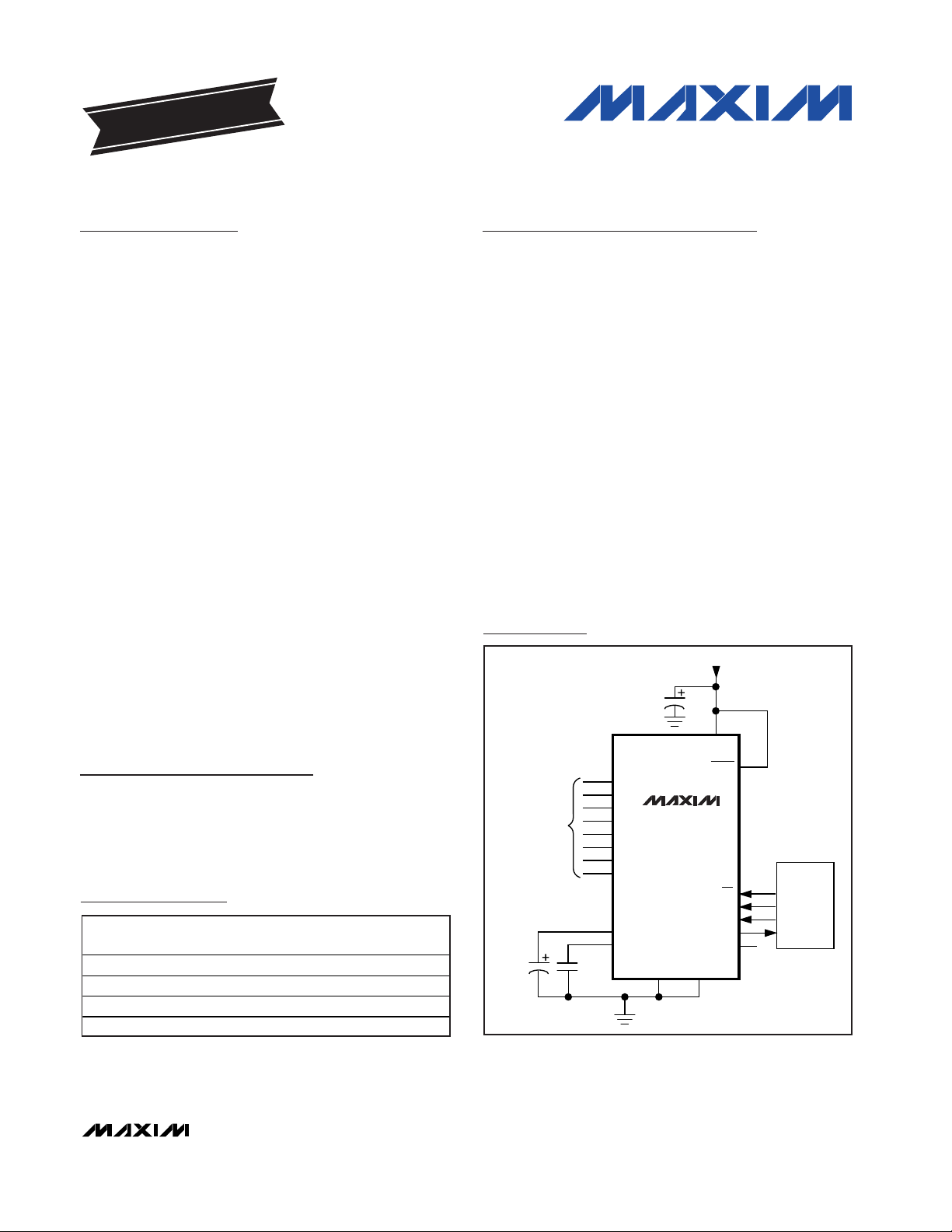
V
DD
CH0
CH1
CH2
CH3
CH4
CH5
CH6
CH7
DGND
4.7µF
0.1µF
0.01µF
SHDN
MAX1270
MAX1271
+5V
ANALOG
INPUTS
CS
SCLK
DIN
DOUT
SSTRB
I/O
SCK
MOSI
MISO
REF
REFADJ
AGND
MC68HCXX
Typical Operating Circuit
PART
TEMP RANGE
PIN-PACKAGE
INL
(LSB)
MAX1270ACNG
±0.5
MAX1270BCNG
±1
MAX1270ACAI
28 SSOP
±0.5
MAX1270BCAI
28 SSOP ±1
Ordering Information
19-4782; Rev 2; 9/04
For pricing, delivery, and ordering information, please contact Maxim/Dallas Direct! at
1-888-629-4642, or visit Maxim’s website at www.maxim-ic.com.
Pin Configurations appear at end of data sheet.
SPI and QSPI are trademarks of Motorola, Inc.
MICROWIRE is a trademark of National Semiconductor Corp.
Ordering Information continued at end of data sheet.
EVALUATION KIT
AVAILABLE
Industrial Control Systems
Data-Acquisition Systems
Battery-Powered
Instruments
Automatic Testing
Robotics
Medical Instruments
0°C to +70°C 24 Narrow PDIP
0°C to +70°C 24 Narrow PDIP
0°C to +70°C
0°C to +70°C
Page 2
MAX1270/MAX1271
Multirange, +5V, 8-Channel,
Serial 12-Bit ADCs
2 _______________________________________________________________________________________
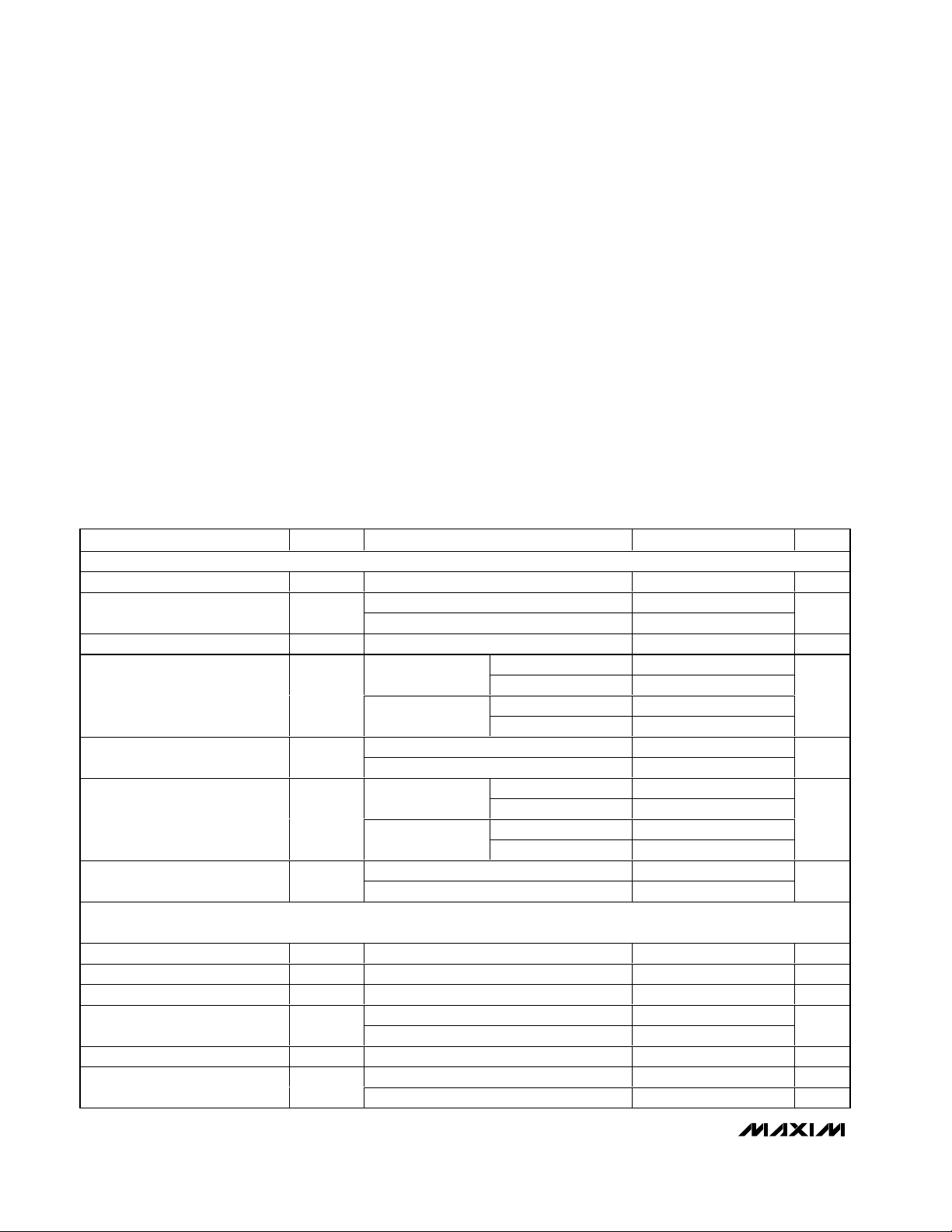
ABSOLUTE MAXIMUM RATINGS
ELECTRICAL CHARACTERISTICS
(VDD= +5.0V ±5%; unipolar/bipolar range; external reference mode, V
REF
= +4.096V; 4.7µF at REF; external clock; f
CLK
= 2.0MHz,
50% duty cycle (MAX127_B); f
CLK
= 1.8MHz, 50% duty cycle (MAX127_A); 18 clock/conversion cycle, TA= T
MIN
to T
MAX
, unless
otherwise noted. Typical values are T
A
= +25°C.)
Stresses beyond those listed under “Absolute Maximum Ratings” may cause permanent damage to the device. These are stress ratings only, and functional
operation of the device at these or any other conditions beyond those indicated in the operational sections of the specifications is not implied. Exposure to
absolute maximum rating conditions for extended periods may affect device reliability.
VDDto AGND............................................................-0.3V to +6V
AGND to DGND.....................................................-0.3V to +0.3V
CH0–CH7 to AGND ......................................................... ±16.5V
REF, REFADJ to AGND ..............................-0.3V to (V
DD
+ 0.3V)
SSTRB, DOUT to DGND.............................-0.3V to (V
DD
+ 0.3V)
SHDN, CS, DIN, SCLK to DGND..............................-0.3V to +6V
Max Current into Any Pin ....................................................50mA
Continuous Power Dissipation (T
A
= +70°C)
24-Pin Narrow DIP (derate 13.33mW/°C above +70°C)..1067mW
28-Pin SSOP (derate 9.52mW/°C above +70°C) ..........762mW
Operating Temperature Ranges
MAX127_C_ _......................................................0°C to +70°C
MAX127_E_ _......................................................-40°C to +85°C
Storage Temperature Range.............................-65°C to +150°C
Lead Temperature (soldering, 10s).................................+300°C
PARAMETER
CONDITIONS
UNITS
ACCURACY (Note 1)
Resolution 12 Bits
MAX127_A
Integral Nonlinearity INL
MAX127_B
LSB
Differential Nonlinearity DNL No missing codes over temperature ±1 LSB
MAX127_A ±3
Unipolar
MAX127_B ±5
MAX127_A ±5
Offset Error
Bipolar
MAX127_B ±10
LSB
Unipolar
Channel-to-Channel Offset Error
Matching
Bipolar
LSB
MAX127_A ±7
Unipolar
MAX127_B ±10
MAX127_A ±7
Gain Error (Note 2)
Bipolar
MAX127_B ±10
LSB
Unipolar, external reference ±3
Gain Error Temperature
Coefficient (Note 2)
Bipolar, external reference ±5
ppm/°C
DYNAMIC SPECIFICATIONS (10kHz sine-wave input, ±10V
P-P
(MAX1270), or ±4.096V
P-P
(MAX1271), f
SAMPLE
= 110ksps
(MAX127_B), f
SAMPLE
= 100ksps (MAX127_A))
SINAD 70 dB
Total Harmonic Distortion THD Up to the 5th harmonic -87 -78 dB
Spurious-Free Dynamic Range SFDR 80 dB
50kHz (Note 3) -86
Channel-to-Channel Crosstalk
DC, V
IN
= ±16.5V -96
dB
Aperture Delay External clock mode 15 ns
External clock mode
ps
Aperture Jitter
Internal clock mode 10 ns
SYMBOL
MIN TYP MAX
±0.5
±1.0
Signal-to-Noise + Distortion Ratio
±0.1
±0.3
<50
Page 3
MAX1270/MAX1271
Multirange, +5V, 8-Channel,
Serial 12-Bit ADCs
_______________________________________________________________________________________ 3
ELECTRICAL CHARACTERISTICS (continued)
(VDD= +5.0V ±5%; unipolar/bipolar range; external reference mode, V
REF
= +4.096V; 4.7µF at REF; external clock; f
CLK
= 2.0MHz,
50% duty cycle (MAX127_B); f
CLK
= 1.8MHz, 50% duty cycle (MAX127_A); 18 clock/conversion cycle, TA= T
MIN
to T
MAX
, unless
otherwise noted. Typical values are T
A
= +25°C.)
PARAMETER
SYMBOL
CONDITIONS
MIN
TYP
MAX
UNITS
ANALOG INPUT
MAX127_A, f
CLK
= 1.8MHz 3.3
Track/Hold Acquisition Time t
ACQ
MAX127_B, f
CLK
= 2.0MHz 3.0
µs
±10V or ±V
REF
range
5
±5V or ±V
REF
/2
range
2.5
0 to 10V or 0 to
V
REF
range
2.5
Small-Signal Bandwidth -3dB rolloff
0 to 5V or 0 to
V
REF
/2 range
MHz
RNG = 1 0 10
MAX1270
RNG = 0 0 5
RNG = 1 0
Unipolar (BIP =
0), Table 3
MAX1271
RNG = 0 0
RNG = 1 -10
MAX1270
RNG = 0 -5 +5
RNG = 1
Input Voltage Range
(Table 3)
V
IN
Bipolar (BIP =
1), Table 3
MAX1271
RNG = 0
+V
REF
/
2
V
0 to 10V
range
-10
MAX1270
0 to 5V
range
-10
Unipolar
MAX1271 -10 0.1
±10V
range
MAX1270
±V
REF
range
Input Current I
IN
Bipolar
MAX1271
±V
REF
/2
range
µA
Unipolar 21
Dynamic Resistance
Bipolar 16
kΩ
Input Capacitance (Note 4) 40 pF
∆VIN/∆I
IN
±5V range -600 +360
1.25
-V
REF
-V
/2
REF
-1200 +720
-1200 +10
-600 +10
V
V
REF
+10
+V
+720
+360
+10
REF
/2
REF
Page 4
MAX1270/MAX1271
Multirange, +5V, 8-Channel,
Serial 12-Bit ADCs
4 _______________________________________________________________________________________
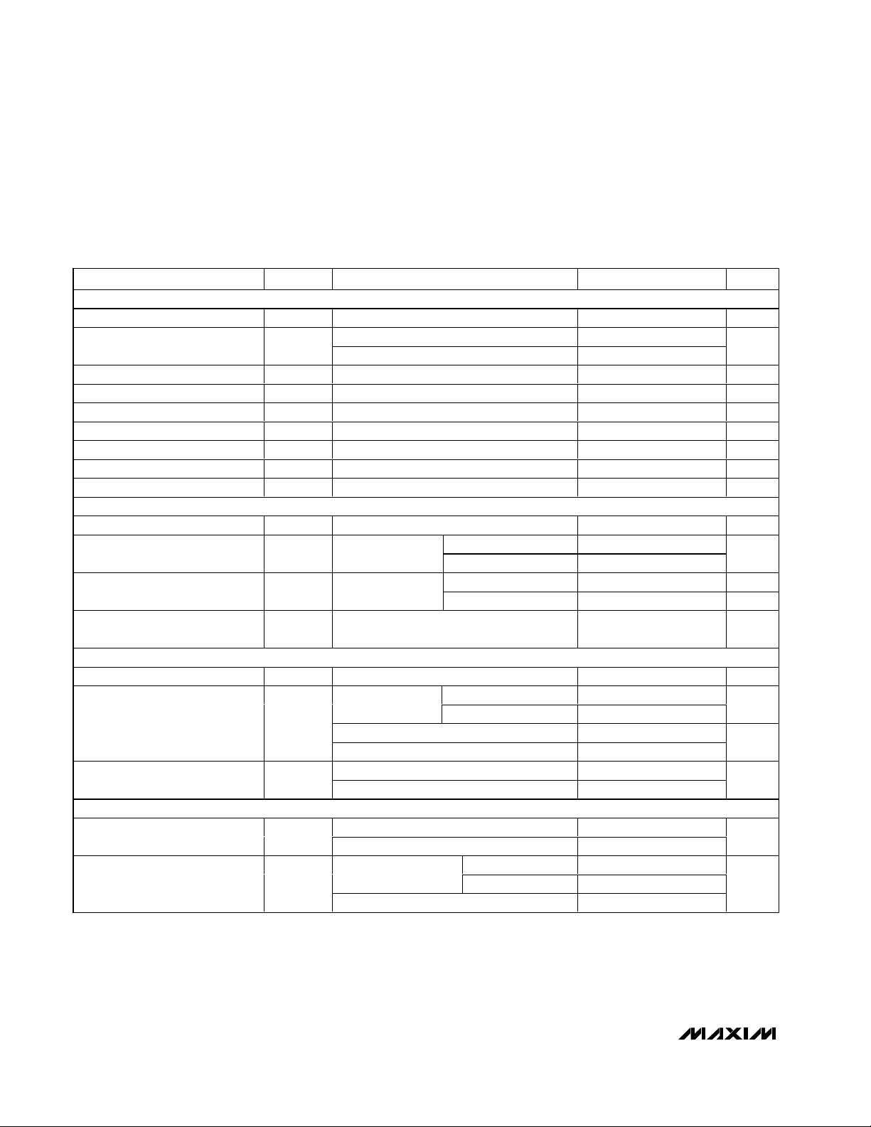
ELECTRICAL CHARACTERISTICS (continued)
(VDD= +5.0V ±5%; unipolar/bipolar range; external reference mode, V
REF
= +4.096V; 4.7µF at REF; external clock; f
CLK
= 2.0MHz,
50% duty cycle (MAX127_B); f
CLK
= 1.8MHz, 50% duty cycle (MAX127_A); 18 clock/conversion cycle, TA= T
MIN
to T
MAX
, unless
otherwise noted. Typical values are T
A
= +25°C.)
PARAMETER
CONDITIONS
UNITS
INTERNAL REFERENCE
REF Output Voltage V
REF
TA = +25°C
V
MAX1270_C/MAX1271_C
REF Output Tempco
MAX1270_E/MAX1271_E
ppm/°C
Output Short-Circuit Current 30 mA
Load Regulation 0 to 0.5mA output current (Note 5) 10 mV
Capacitive Bypass at REF 4.7 µF
Capacitive Bypass at REFADJ
µF
REFADJ Output Voltage
V
REFADJ Adjustment Range Figure 1
%
Buffer Voltage Gain
V/V
REFERENCE INPUT (Reference buffer disabled, reference input applied to REF)
Input Voltage Range
V
Normal or STBYPD 400
Input Current V
REF
= 4.18V
FULLPD 1
µA
Normal or STBYPD 10 kΩ
Input Resistance V
REF
= 4.18V
FULLPD
MΩ
REFADJ Threshold for Buffer
Disable
VDD -
0.5
V
POWER REQUIREMENT
Supply Voltage V
DD
V
Bipolar range 18
Normal
Unipolar range 6 10
mA
STBYPD power-down mode (Note 6)
850
Supply Current I
DD
FULLPD power-down mode
220
µA
External reference = 4.096V
Power-Supply Rejection
Ratio (Note 7)
PSRR
Internal reference
LSB
TIMING
MAX127_A 0.1 1.8
External Clock Frequency Range
f
SCLK
MAX127_B 0.1 2.0
MHz
MAX127_A 3.3
External clock mode
(Note 8)
MAX127_B 3.0
Acquisition Phase
Internal clock mode, Figure 9 3 5
µs
SYMBOL
TC V
REF
MIN TYP MAX
4.076 4.096 4.116
0.01
2.465 2.500 2.535
2.40 4.18
4.18
4.75 5.25
±15
±30
±1.5
1.638
700
120
±0.1 ±0.5
±0.5
Page 5
MAX1270/MAX1271
Multirange, +5V, 8-Channel,
Serial 12-Bit ADCs
_______________________________________________________________________________________ 5
ELECTRICAL CHARACTERISTICS (continued)
(VDD= +5.0V ±5%; unipolar/bipolar range; external reference mode, V
REF
= +4.096V; 4.7µF at REF; external clock; f
CLK
= 2.0MHz,
50% duty cycle (MAX127_B); f
CLK
= 1.8MHz, 50% duty cycle (MAX127_A); 18 clock/conversion cycle, TA= T
MIN
to T
MAX
, unless
otherwise noted. Typical values are T
A
= +25°C.)
PARAMETER
CONDITIONS
UNITS
MAX127_A 6.6
External clock mode
(Note 8)
MAX127_B 6.0
Conversion Time t
CONV
Internal clock mode, Figure 9 6 7.7 11
µs
MAX127_A 100
External clock mode
MAX127_B 110
Throughput Rate
Internal clock mode 43
ksps
Bandgap Reference Startup Time
Power-up (Note 9)
µs
C
REF
= 4.7µF 8
Reference Buffer Settling Time
To 0.1mV, REF bypass
capacitor fully
discharged
C
REF
= 33µF 60
ms
DIGITAL INPUTS (DIN, SCLK, CS, and SHDN)
Input High Threshold Voltage V
IH
2.4 V
Input Low Threshold Voltage V
IL
0.8 V
Input Hysteresis V
HYS
0.2 V
Input Leakage Current I
IN
VIN = 0 to V
DD
-10
µA
Input Capacitance C
IN
(Note 4) 15 pF
DIGITAL OUTPUTS (DOUT, SSTRB)
I
SINK
= 5mA 0.4
Output Voltage Low V
OL
I
SINK
= 16mA 0.4
V
Output Voltage High V
OH
I
SOURCE
= 0.5mA
V
DD -
0.5
V
Tri-State Leakage Current I
L
CS = V
DD
-10
µA
Tri-State Output Capacitance C
OUT
CS = V
DD
(Note 4) 15 pF
SYMBOL
MIN TYP MAX
200
+10
+10
Page 6
MAX1270/MAX1271
Multirange, +5V, 8-Channel,
Serial 12-Bit ADCs
6 _______________________________________________________________________________________
Note 1: Accuracy specifications tested at VDD= +5.0V. Performance at power-supply tolerance limit is guaranteed by power-supply
rejection test.
Note 2: External reference: V
REF
= 4.096V, offset error nulled. Ideal last-code transition = FS - 3/2 LSB.
Note 3: Ground “on” channel; sine wave applied to all “off” channels. V
IN
= ±5V (MAX1270), VIN= ±4V (MAX1271).
Note 4: Guaranteed by design, not production tested.
Note 5: Use static external loads during conversion for specified accuracy.
Note 6: Tested using internal reference.
Note 7: PSRR measured at full scale. Tested for the ±10V (MAX1270) and ±4.096V (MAX1271) input ranges.
Note 8: Acquisition phase and conversion time are dependent on the clock period; clock has 50% duty cycle (Figure 6).
Note 9: Not production tested. Provided for design guidance only.
TIMING CHARACTERISTICS
(VDD= +4.75V to +5.25V; unipolar/bipolar range; external reference mode, V
REF
= +4.096V; 4.7µF at REF; external clock; f
CLK
=
2.0MHz (MAX127_B); f
CLK
= 1.8MHz (MAX127_A); TA= T
MIN
to T
MAX
, unless otherwise noted. Typical values are TA= +25°C.)
(Figures 2, 5, 7, 10)
PARAMETER
SYMBOL
CONDITIONS
MIN
TYP
MAX
UNITS
DIN to SCLK Setup t
DS
ns
DIN to SCLK Hold t
DH
0ns
SCLK Fall to Output Data Valid t
DO
20
ns
CS Fall to Output Enable t
DV
C
LOAD
= 100pF
ns
CS Rise to Output Disable t
TR
C
LOAD
= 100pF
ns
CS to SCLK Rise Setup t
CSS
ns
CS to SCLK Rise Hold t
CSH
0ns
SCLK Pulse-Width High t
CH
ns
SCLK Pulse-Width Low t
CL
ns
SCLK Fall to SSTRB t
SSTRB
C
LOAD
= 100pF
ns
CS to SSTRB Output Enable t
SDV
C
LOAD
= 100pF, external clock mode only
ns
CS to SSTRB Output Disable t
STR
C
LOAD
= 100pF, external clock mode only
ns
SSTRB Rise to SCLK Rise t
SCK
Internal clock mode only (Note 4) 0 ns
100
100
200
200
170
120
100
200
200
200
Page 7

MAX1270/MAX1271
Multirange, +5V, 8-Channel,
Serial 12-Bit ADCs
_______________________________________________________________________________________ 7
Typical Operating Characteristics
(Typical Operating Circuit, VDD= +5V; external reference mode, V
REF
= +4.096V; 4.7µF at REF; external clock, f
CLK
= 2MHz;
110ksps; TA= +25°C, unless otherwise noted.)
0
5
15
10
20
25
021 34567
SUPPLY CURRENT vs. SUPPLY VOLTAGE
MAX1270/1 toc01
SUPPLY VOLTAGE (V)
SUPPLY CURRENT (mA)
5.5
5.7
6.1
5.9
6.3
6.5
-40 10-15 35 60 85
SUPPLY CURRENT vs. TEMPERATURE
MAX1270/1 toc02
TEMPERATURE (°C)
SUPPLY CURRENT (mA)
50
150
450
350
250
650
550
750
-40 10-15 35 60 85
STANDBY SUPPLY CURRENT
vs. TEMPERATURE
MAX1270/1 toc03
TEMPERATURE (°C)
STANDBY SUPPLY CURRENT (µA)
INTERNAL
REFERENCE
EXTERNAL
REFERENCE
50
70
110
90
130
150
-40 10-15 35 60 85
FULL POWER-DOWN SUPPLY CURRENT
vs. TEMPERATURE
MAX1270/1 toc04
TEMPERATURE (°C)
FULL POWER-DOWN SUPPLY CURRENT (µA)
INTERNAL
REFERENCE
EXTERNAL
REFERENCE
0.1
0.2
0.6
0.5
0.4
0.3
0.7
0.8
-40 10-15 35 60 85
CHANNEL-TO-CHANNEL GAIN-ERROR
MATCHING vs. TEMPERATURE
MAX1270/1 toc07
TEMPERATURE (°C)
CHANNEL-TO-CHANNEL GAIN-ERROR MATCHING (LSB)
BIPOLAR MODE
UNIPOLAR MODE
0.996
0.997
0.999
0.998
1.000
1.001
-40 10-15 35 60 85
NORMALIZED REFERENCE VOLTAGE
vs. TEMPERATURE
MAX1270/1 toc05
TEMPERATURE (°C)
NORMALIZED REFERENCE VOLTAGE
0
0.05
0.25
0.20
0.15
0.10
0.30
0.35
-40 10-15 35 60 85
CHANNEL-TO-CHANNEL OFFSET-ERROR
MATCHING vs. TEMPERATURE
MAX1270/1 toc06
TEMPERATURE (°C)
CHANNEL-TO-CHANNEL OFFSET-ERROR MATCHING (LSB)
BIPOLAR MODE
UNIPOLAR MODE
-0.15
-0.10
0.05
0
-0.05
0.10
0.15
0 1638819 2457 3276 4095
INTEGRAL NONLINEARITY vs.
DIGITAL CODE
MAX1270/1 toc08
DIGITAL CODE
INTEGRAL NONLINEARITY (LSB)
-120
-100
-40
-60
-80
-20
0
0 20k10k 30k 40k 50k
FTT PLOT
MAX1270/1 toc09
FREQUENCY (Hz)
AMPLITUDE (dB)
fIN = 10kHz
f
SAMPLE
= 110ksps
Page 8

MAX1270/MAX1271
Multirange, +5V, 8-Channel,
Serial 12-Bit ADCs
8 _______________________________________________________________________________________
Pin Description
PIN
PDIP
NAME FUNCTION
11 VDD+5V Supply. Bypass with a 0.1µF capacitor to AGND.
2, 4
2, 3 DGND Digital Ground
3, 9,
22, 24
4, 7, 8,
11, 22,
N.C. No Connection. No internal connection.
55SCLK
Serial Clock Input. Clocks data in and out of serial interface. In external clock mode, SCLK also
sets the conversion speed.
66 CS
Active-Low Chip-Select Input. Data is not clocked into DIN unless CS is low. When CS is high,
DOUT is high impedance.
79 DIN Serial Data Input. Data is clocked in on the rising edge of SCLK.
810
Serial Strobe Output. In internal clock mode, SSTRB goes low after the falling edge of the eighth
SCLK and returns high when the conversion is done. In external clock mode, SSTRB pulses high
for one clock period before the MSB decision. High impedance when CS is high in external
clock mode.
10
12 DOUT
Serial Data Output. Data is clocked out on the falling edge of SCLK. High impedance when CS is
high.
11
13 SHDN Shutdown Input. When low, device is in FULLPD mode. Connect high for normal operation.
12
14 AGND Analog Ground
13–20
Analog Input Channels
21
26
Bandgap Voltage-Reference Output/External Adjust Pin. Bypass with a 0.01µF capacitor to AGND.
Connect to V
DD
when using an external reference at REF.
23
27 REF
Refer ence- Buffer O utp ut/AD C Refer ence Inp ut. In i nter nal r efer ence m od e, the r efer ence b uffer
p r ovi d es a 4.096V nom i nal outp ut, exter nal l y ad j ustab l e to RE FAD J. In exter nal r efer ence m od e,
d i sab l e the i nter nal r efer ence b y p ul l i ng RE FAD J to V
D D
and ap p l yi ng the exter nal r efer ence to RE F.
Typical Operating Characteristics (continued)
(Typical Operating Circuit, VDD= +5V; external reference mode, V
REF
= +4.096V; 4.7µF at REF; external clock, f
CLK
= 2MHz;
110ksps; T
A
= +25°C, unless otherwise noted.)
AVERAGE SUPPLY CURRENT vs.
CONVERSION RATE (USING STANDBY)
8
VDD = 5V, INTERNAL REFERENCE,
= 2MHz
f
7
CLK
EXTERNAL CLOCK MODE.
LOW-RANGE UNIPOLAR MODE.
6
= 0
V
CH_
5
4
3
2
AVERAGE SUPPLY CURRENT (mA)
1
0
0.1 1 10 100 1000
CONVERSION RATE (ksps)
SSOP
MAX1270-toc10
AVERAGE SUPPLY CURRENT vs.
CONVERSION RATE (USING FULLPD)
8
VDD = 5V, INTERNAL REFERENCE,
f
= 2MHz
7
CLK
EXTERNAL CLOCK MODE.
LOW-RANGE UNIPOLAR MODE.
6
= 0
V
CH_
5
4
3
2
AVERAGE SUPPLY CURRENT (mA)
1
0
0.1 1 10 100 1000
CONVERSION RATE (ksps)
MAX1270-toc11
24, 25, 28
SSTRB
15–21, 23 CH0–CH7
REFADJ
Page 9

MAX1270/MAX1271
Multirange, +5V, 8-Channel,
Serial 12-Bit ADCs
_______________________________________________________________________________________ 9
Detailed Description
Converter Operation
The MAX1270/MAX1271 multirange, fault-tolerant ADCs
use successive approximation and internal track/hold
(T/H) circuitry to convert an analog signal to a 12-bit
digital output. Figure 3 shows the block diagram of the
MAX1270/MAX1271.
Analog-Input Track/Hold
The T/H enters tracking/acquisition mode on the falling
edge of the sixth clock in the 8-bit input control word,
and enters hold/conversion mode when the timed
acquisition interval (six clock cycles, 3µs minimum)
ends. In internal clock mode, the acquisition is timed by
two external clock cycles and four internal clock cycles.
When operating in bipolar (MAX1270 and MAX1271) or
unipolar mode (MAX1270) the signal applied at the
input channel is rescaled through the resistor-divider
network formed by R1, R2, and R3 (Figure 4); a low
impedance (<4Ω) input source is recommended to
minimize gain error. When the MAX1271 is configured
for unipolar mode, the channel input resistance (RIN)
becomes a fixed 5.12kΩ (typ). Source impedances
below 15kΩ (0 to V
REF
) and 5kΩ (0 to V
REF
/2) do not
significantly affect the AC performance of the ADC.
The acquisition time (t
ACQ
) is a function of the source
output resistance, the channel input resistance, and the
T/H capacitance. Higher source impedances can be
used if an input capacitor is connected between the
analog inputs and AGND. Note that the input capacitor
forms an RC filter with the input source impedance, limiting the ADC’s signal bandwidth.
100kΩ
510kΩ
24kΩ
REFADJ
+5V
MAX1270
MAX1271
0.01µF
Figure 1. Reference-Adjust Circuit
Figure 3. Block Diagram
Figure 2. Output Load Circuit for Timing Characteristics
+5V
DOUT
OR
SSTRB
C
0.5mA
a)
HIGH IMPEDANCE TO V
AND VOH TO HIGH IMPEDANCE
V
OH
LOAD
OH
, VOL TO
5mA
DOUT
OR
SSTRB
b)
HIGH IMPEDANCE TO V
AND VOH TO HIGH IMPEDANCE
V
OH
DIN
SSTRB DOUT CS SCLK
C
LOAD
, VOL TO
OH
SHDN
CH0
CH1
CH2
CH3
CH4
CH5
CH6
CH7
REF
REFADJ
CLOCK
INT
CLOCK
ANALOG
INPUT
MUX
AND SIGNAL
CONDITIONING
2.5V
REFERENCE
10kΩ
SERIAL INTERFACE LOGIC
T/H
+4.096V
Av =
1.638
OUT
IN
12-BIT SAR ADC
REF
MAX1270
MAX1271
V
DD
AGND
DGND
Page 10
MAX1270/MAX1271
Multirange, +5V, 8-Channel,
Serial 12-Bit ADCs
10 ______________________________________________________________________________________
Input Bandwidth
The ADC’s input small-signal bandwidth depends on the
selected input range and varies from 1.5MHz to 5MHz
(see Electrical Characteristics). The MAX1270B/
MAX1271B maximum sampling rate is 110ksps (100ksps
for the MAX1270A/MAX1271A). By using undersampling
techniques, it is possible to digitize high-speed transient
events and measure periodic signals with bandwidths
exceeding the ADC’s sampling rate.
To avoid high-frequency signals being aliased into the
frequency band of interest, anti-aliasing filtering is recommended.
Input Range and Protection
The MAX1270/MAX1271 have software-selectable input
ranges. Each analog input channel can be independently programmed to one of four ranges by setting the
appropriate control bits (RNG, BIP) in the control byte
(Table 1). The MAX1270 has selectable input ranges
extending to ±10V (±V
REF
x 2.441), while the MAX1271
has selectable input ranges extending to ±V
REF
. Figure
4 shows the equivalent input circuit.
A resistor network on each analog input provides
±16.5V fault protection for all channels. Whether or not
the channel is on, this circuit limits the current going
into or out of the pin to less than 2mA. This provides an
added layer of protection when momentary overvoltages occur at the selected input channel, when a negative signal is applied to the input, and when the device
is configured for unipolar mode. The overvoltage protection is active even if the device is in power-down
mode or if VDD= 0.
Digital Interface
The MAX1270/MAX1271 feature a serial interface that is
fully compatible with SPI/QSPI and MICROWIRE devices.
For SPI/QSPI, set CPOL = 0, CPHA = 0 in the SPI control
registers of the microcontroller. Figure 5 shows detailed
serial-interface timing information. See Table 1 for details
on programming the input control byte.
t
CSH
t
CSS
t
CL
t
DS
t
DH
t
DV
t
CH
t
DO
t
TR
t
CSH
CS
SCLK
DIN
DOUT
Figure 5. Detailed Serial-Interface Timing
R3
5.12kΩ
R2
R1
CH_
S1
S2
S3
S4
BIPOLAR
UNIPOLAR
VOLTAGE
REFERENCE
T/H
OUT
HOLDTRACK
TRACKHOLD
OFF
ON
C
HOLD
S1 = BIPOLAR/UNIPOLAR SWITCH
S2 = INPUT MUX SWITCH
S3, S4 = T/H SWITCH
R1 = 12.5kΩ (MAX1270)
or 5.12kΩ (MAX1271)
R2 = 8.67kΩ (MAX1270)
or ∞ (MAX1271)
Figure 4. Equivalent Input Circuit
Page 11
MAX1270/MAX1271
Multirange, +5V, 8-Channel,
Serial 12-Bit ADCs
______________________________________________________________________________________ 11
Table 1. Control-Byte Format
BIT 7
(MSB)
BIT 6 BIT 5 BIT 4 BIT 3 BIT 2 BIT 1
BIT 0
(LSB)
START SEL2 SEL1 SEL0 RNG BIP PD1 PD0
BIT NAME DESCRIPTION
7 (MSB) START First logic 1 after CS goes low defines the beginning of the control byte.
6, 5, 4
SEL2, SEL1,
SEL0
These 3 bits select the desired “on” channel (Table 2).
3 RNG Selects the full-scale input voltage range (Table 3).
2 BIP Selects the unipolar or bipolar conversion mode (Table 3).
1, 0 (LSB) PD1, PD0 Select clock and power-down modes (Table 4).
Table 2. Channel Selection
SEL2 SEL1 SEL0 CHANNEL
000 CH0
001 CH1
010 CH2
011 CH3
100 CH4
101 CH5
110 CH6
111 CH7
Table 4. Power-Down and Clock Selection
PD1
PD0
MODE
00
Normal operation (always on), internal clock
mode.
01
Normal operation (always on), external clock
mode.
10
Standby power-down mode (STBYPD), clock
mode unaffected.
11
Full power-down mode (FULLPD), clock mode
unaffected.
Table 3. Range and Polarity Selection for MAX1270/MAX1271
RANGE AND POLARITY SELECTION FOR THE MAX1270
INPUT RANGE RNG BIP
Negative
FULL SCALE
ZERO
SCALE (V)
FULL SCALE
0 to +5V 0 0 — 0 V
REF
x 1.2207
0 to +10V 1 0 — 0 V
REF
x 2.4414
±5V 0 1 -V
REF
x 1.2207 0 V
REF
x 1.2207
±10V 1 1 -V
REF
x 2.4414 0 V
REF
x 2.4414
RANGE AND POLARITY SELECTION FOR THE MAX1271
INPUT RANGE RNG BIP
Negative
FULL SCALE
ZERO
SCALE (V)
FULL SCALE
0 to V
REF
/2 0 0 — 0 V
REF
/2
0 to V
REF
10 — 0 V
REF
±V
REF
/2 0 1 -V
REF
/2 0 V
REF
/2
±V
REF
11 -V
REF
0V
REF
Page 12

MAX1270/MAX1271
Multirange, +5V, 8-Channel,
Serial 12-Bit ADCs
12 ______________________________________________________________________________________
Input Data Format
Input data (control byte) is clocked in at DIN at the rising edge of SCLK. CS enables communication with the
MAX1270/MAX1271. After CS falls, the first arriving
logic 1 bit represents the start bit (MSB) of the input
control byte. The start bit is defined as:
The first high bit clocked into DIN with CS low
anytime the converter is idle; e.g., after VDDis
applied.
OR
The first high bit clocked into DIN after bit 6
(D6) of a conversion in progress is clocked
onto DOUT.
Output Data Format
Output data is clocked out on the falling edge of SCLK
at DOUT, MSB first (D11). In unipolar mode, the output
is straight binary. For bipolar mode, the output is two’s
complement binary. For output binary codes, refer to
the Transfer Function section.
How to Start a Conversion
The MAX1270/MAX1271 use either an external serial
clock or the internal clock to complete an acquisition
and perform a conversion. In both clock modes, the
external clock shifts data in and out. See Table 4 for
details on programming clock modes.
The falling edge of CS does not start a conversion on
the MAX1270/MAX1271; a control byte is required for
each conversion. Acquisition starts after the sixth bit is
programmed in the input control byte. Conversion
starts when the acquisition time, six clock cycles,
expires.
Keep CS low during successive conversions. If a startbit is received after CS transitions from high to low, but
before the output bit 6 (D6) becomes available, the current conversion will terminate and a new conversion will
begin.
External Clock Mode (PD1 = 0, PD0 = 1)
In external clock mode, the clock shifts data in and out
of the MAX1270/MAX1271 and controls the acquisition
and conversion timings. When acquisition is done,
SSTRB pulses high for one clock cycle and conversion
begins. Successive-approximation bit decisions appear
at DOUT on each of the next 12 SCLK falling edges
(Figure 6). Additional SCLK falling edges will result in
zeros appearing at DOUT. Figure 7 shows the SSTRB
timing in external clock mode.
SSTRB and DOUT go into a high-impedance state
when CS goes high; after the next CS falling edge,
SSTRB and DOUT will output a logic low.
The conversion must be completed in some minimum
time, or droop on the sample-and-hold capacitors may
degrade conversion results. Use internal clock mode if
the clock period exceeds 10µs, or if serial-clock interruptions could cause the conversion interval to exceed
120µs. The fastest the MAX1270/MAX1271 can run is
18 clocks per conversion in external clock mode, and
with a clock rate of 2MHz, the maximum sampling rate
is 111 ksps (Figure 8). In order to achieve maximum
throughput, keep CS low, use external clock mode with
a continuous SCLK, and start the following control byte
after bit 6 (D6) of the conversion in progress is clocked
onto DOUT.
If CS is low and SCLK is continuous, guarantee a start
bit by first clocking in 18 zeros.
SSTRB
CS
SCLK
DIN
DOUT
181213 14 24 25
START
SEL2 SEL1 SEL0 BIPRNG PD1 PD0
LSB
D11
MSB
MSB
D10 D9 D1 D0
LSB
ACQUISITION
6 SCLK
FILLED WITH
ZEROS
CONVERSION
12 SCLK
A/D STATE
HIGH-Z
HIGH-Z
HIGH-Z
HIGH-Z
Figure 6. External Clock Mode—25 Clocks/Conversion Timing
Page 13

MAX1270/MAX1271
Multirange, +5V, 8-Channel,
Serial 12-Bit ADCs
______________________________________________________________________________________ 13
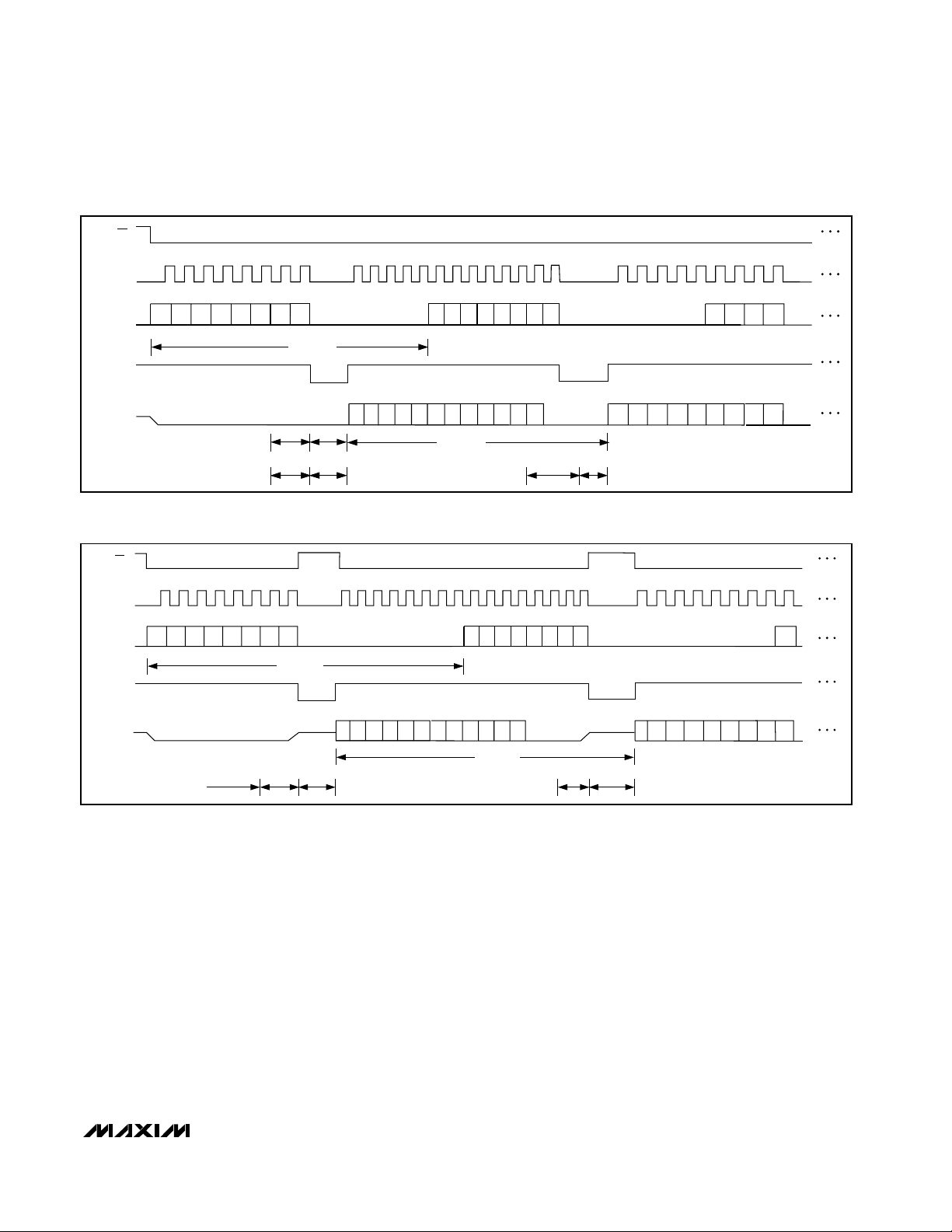
Internal Clock Mode (PD1 = 0, PD0 = 0)
In internal clock mode, the MAX1270/MAX1271 generate their conversion clock internally. This frees the
microprocessor from the burden of running the acquisition and the SAR conversion clock, and allows the conversion results to be read back at the processor’s
convenience, at any clock rate from 0 to typically
10MHz.
SSTRB goes low after the falling edge of the last bit
(PD0) of the control byte has been shifted in, and
returns high when the conversion is complete.
Acquisition is completed and conversion begins on the
falling edge of the 4th internal clock pulse after the control byte; conversion ends on the falling edge of the
16th internal clock pulse (12 internal clock cycle pulses
are used for conversion). SSTRB will remain low for a
maximum of 15µs, during which time SCLK should
remain low for best noise performance. An internal register stores data while the conversion is in progress.
The MSB of the result byte (D11) is present at DOUT
starting at the falling edge of the last internal clock of
conversion. Successive falling edges of SCLK will shift
the remaining data out of this register (Figure 9).
Additional SCLK edges will result in zeros on DOUT.
When internal clock mode is selected, SSTRB does not
go into a high-impedance state when CS goes high.
Pulling CS high prevents data from being clocked in
and tri-states DOUT, but does not adversely affect a
t
SDV
t
SSTRB
SCLK 12
t
STR
SSTRB
SCLK
CS
t
SSTRB
HIGH-Z HIGH-Z
Figure 7. External Clock Mode—SSTRB Detailed Timing
CS
SCLK
DIN
DOUT
A/D STATE
13
19 24 26 31 32
14
16
37
START
SEL2 SEL1 SEL0
BIPRNG PD1 PD0
D11 D10 D9 D7D8 D6 D5 D4 D2D3 D1 D0
LSB
81
MSB
LSBMSB
START
SEL2 SEL1 SEL0
BIPRNG PD1 PD0
START
SEL2
CONTROL BYTE 0
RESULT
CONTROL BYTE 1 CONTROL BYTE 2
18 SCLK
18 SCLK
SSTRB
D10D11 D9 D8 D6D7 D5
RESULT 1
ACQUISITION
6 SCLK
CONVERSION
12 SCLK
ACQUISITION
6 SCLK
CONVERSION
12 SCLK
HIGH-Z
HIGH-Z
Figure 8. External Clock Mode—18 Clocks/Conversion Timing
Page 14

MAX1270/MAX1271
Multirange, +5V, 8-Channel,
Serial 12-Bit ADCs
14 ______________________________________________________________________________________
conversion in progress. Figure 10 shows the SSTRB
timing in internal clock mode.
Internal clock mode conversions can be completed
with 13 external clocks per conversion but require a
waiting period of 15µs for the conversion to be completed (Figure 11).
Most microcontrollers require that conversions occur in
multiples of 8 SCLK clock cycles. Sixteen clock cycles
per conversion (as shown in Figure 12) is typically the
most convenient way for a microcontroller to drive the
MAX1270/MAX1271.
Applications Information
Power-On Reset
The MAX1270/MAX1271 power up in normal operation
(all internal circuitry active) and internal clock mode,
waiting for a start bit. The contents of the output data
register are cleared at power-up.
Internal or External Reference
The MAX1270/MAX1271 operate with either an internal
or external reference. An external reference is connected to either REF or REFADJ (Figure 13). The REFADJ
internal buffer gain is trimmed to 1.638V to provide
4.096V at REF from a 2.5V reference.
SSTRB
CS
SCLK
DIN
DOUT
1
8
20
START
SEL2 SEL1 SEL0 RNG BIP PD1 PD0
D11 D10 D1 D0
ACQUISITION
FILLED WITH ZEROS
CONVERSION
A/D STATE
910 19
16 INT CLK
12 INT CLK
MSB LSB
MSB LSB
2 EXT SCLK
+4 INT CLK
HIGH-Z HIGH-Z HIGH-Z
Figure 9. Internal Clock Mode—20 SCLK/Conversion Timing
SCLK #8
t
SSTRB
t
CSH
t
SCK
t
CSS
NOTE: FOR BEST NOISE PERFORMANCE, KEEP SCLK LOW DURING CONVERSION.
SSTRB
SCLK
CS
Figure 10. Internal Clock Mode—SSTRB Detailed Timing
Page 15
MAX1270/MAX1271
Multirange, +5V, 8-Channel,
Serial 12-Bit ADCs
______________________________________________________________________________________ 15
Internal Reference
The internally trimmed 2.50V reference is amplified
through the REFADJ buffer to provide 4.096V at REF.
Bypass REF with a 4.7µF capacitor to AGND and
REFADJ with a 0.01µF capacitor to AGND (Figure 13a).
The internal reference voltage is adjustable to ±1.5%
(±65 LSBs) with the reference-adjust circuit of Figure 1.
External Reference
To use the REF input directly, disable the internal buffer
by tying REFADJ to VDD(Figure 13b). Using the
REFADJ input eliminates the need to buffer the reference externally. When a reference is applied at
REFADJ, bypass REFADJ with a 0.01µF capacitor to
AGND. Note that when an external reference is applied
at REFADJ, the voltage at REF is given by:
V
REF
= 1.6384 x V
REFADJ
(2.4 < V
REF
< 4.18)
(Figure 13c). At REF and REFADJ, the input impedance
is a minimum of 10kΩ for DC currents. During conversions, an external reference at REF must be able to deliver 400µA DC load currents and must have an output
impedance of 10Ω or less. If the reference has higher
output impedance or is noisy, bypass REF with a 4.7µF
capacitor to AGND as close to the chip as possible.
With an external reference voltage of less than 4.096V
at REF or less than 2.5V at REFADJ, the increase in the
ratio of RMS noise to the LSB value (full-scale / 4096)
results in performance degradation (loss of effective
bits).
CS
SCLK
DIN
DOUT
A/D STATE
1
8
9
242214
16
START
SEL2 SEL1 SEL0
BIP
RNG
PD1 PD0
D11 D10 D9 D7D8 D6 D5 D4 D2D3 D1 D0
START
SEL2 SEL1 SEL0
BIP
RNG
PD1 PD0
START
SEL0SEL1SEL2
CONTROL BYTE Ø
RESULT Ø
CONTROL BYTE 1 CONTROL BYTE 2
13 SCLK
13 SCLK
SSTRB
D10D11 D9 D8 D6D7 D5 D4 D3
RESULT 1
ACQUISITION
CONVERSION
ACQUISITION
CONVERSION
HIGH-Z
Figure 11. Internal Clock Mode—13 Clocks/Conversion Timing
CS
SCLK
DIN
DOUT
A/D STATE
IDLE
9 24
25 32
16 17
START
START
SEL2 SEL1 SEL0 BIPRNG PD1 PD0
D11 D10 D9 D7D8 D6 D5 D4 D2D3 D1 D0
START
SEL2 SEL1 SEL0 BIPRNG PD1 PD0
CONTROL BYTE Ø
RESULT Ø
CONTROL BYTE 1 CB 2
16 SCLK
16 SCLK
SSTRB
D10
D11
D9 D8 D6D7 D5 D4 D3
RESULT 1
ACQUISITION CONVERSION ACQUISITION CONVERSION
HIGH-ZHIGH-Z HIGH-Z
1
8
Figure 12. Internal Clock Mode—16 Clocks/Conversion Timing
Page 16

MAX1270/MAX1271
Multirange, +5V, 8-Channel,
Serial 12-Bit ADCs
16 ______________________________________________________________________________________
Power-Down Mode
To save power, configure the converter into low-current
shutdown mode between conversions. Two programmable power-down modes are available in addition to a
hardware shutdown. Select STBYPD or FULLPD by programming PD0 and PD1 in the input control byte
(Table 4). When software power-down is asserted, it
becomes effective only after the end of conversion. For
example, if the control byte contains PD1 = 0, then the
chip remains powered up. If PD1 = 1, then the chip
powers down at the end of conversion. In all powerdown modes, the interface remains active and conversion results can be read. Input overvoltage protection is
active in all power-down modes.
The first logical 1 on DIN after CS falls is interpreted as
a start condition, and powers up the MAX1270/
MAX1271 from a software selected STBYPD or FULLPD
condition.
For hardware-controlled power-down (FULLPD), pull
SHDN low. When hardware shutdown is asserted, it
becomes effective immediately, and any conversion in
progress is aborted.
Choosing Power-Down Modes
The bandgap reference and reference buffer remain
active in STBYPD mode, maintaining the voltage on the
4.7µF capacitor at REF. This is a DC state that does not
degrade after power-down of any duration.
In FULLPD mode, only the bandgap reference is active.
Connect a 33µF capacitor between REF and AGND to
maintain the reference voltage between conversions
and to reduce transients when the buffer is enabled
and disabled. Throughput rates down to 1ksps can be
achieved without allotting extra acquisition time for reference recovery prior to conversion. This allows conversion to begin immediately after power-up. If the
discharge of the REF capacitor during FULLPD
exceeds the desired limits for accuracy (less than a
fraction of an LSB), run a STBYPD power-down cycle
prior to starting conversions. Take into account that the
reference buffer recharges the bypass capacitor at an
80mV/ms slew rate, and add 50µs for settling time.
Auto-Shutdown
Selecting STBYPD on every conversion automatically
shuts down the MAX1270/MAX1271 after each conversion
without requiring any start-up time on the next conversion.
REF
10kΩ
2.5V
2.5V
REFADJ
A
V
= 1.638
MAX1270
MAX1271
4.7µF
C
REF
0.01µF
Figure 13c. External Reference—Reference at REFADJ
REF
V
DD
10kΩ
2.5V
4.096V
REFADJ
A
V
= 1.638
MAX1270
MAX1271
4.7µF
C
REF
Figure 13b. External Reference—Reference at REF
REF
10kΩ
2.5V
REFADJ
0.01µF
A
V
= 1.638
MAX1270
MAX1271
4.7µF
C
REF
Figure 13a. Internal Reference
Page 17

MAX1270/MAX1271
Multirange, +5V, 8-Channel,
Serial 12-Bit ADCs
______________________________________________________________________________________ 17
Transfer Function
Output data coding for the MAX1270/MAX1271 is binary in unipolar mode with 1 LSB = (FS / 4096) and two’s
complement binary in bipolar mode with 1 LSB = [(2 x
| FS | ) / 4096]. Code transitions occur halfway between
successive-integer LSB values. Figures 14a and 14b
show the input/output (I/O) transfer functions for unipo-
lar and bipolar operations, respectively. For full-scale
values, refer to Table 3.
Layout, Grounding, and Bypassing
Careful PC board layout is essential for best system
performance. Use a ground plane for best perfor-
mance. To reduce crosstalk and noise injection, keep
analog and digital signals separate. Connect analog
grounds and DGND in a star configuration to AGND.
For noise-free operation, ensure the ground return from
AGND to the supply ground is low impedance and as
short as possible. Connect the logic grounds directly to
the supply ground. Bypass V
DD
with 0.1µF and 4.7µF
capacitors to AGND to minimize highand low-frequency
fluctuations. If the supply is excessively noisy, connect
a 5Ω resistor between the supply and VDD, as shown in
Figure 15.
V
DD
GND
DGND
DGNDAGND
+5V
+5V
SUPPLY
R* = 5Ω
DIGITAL
CIRCUITRY
4.7µF
0.1µF
MAX1270
MAX1271
**
*OPTIONAL
**CONNECT AGND AND DGND WITH A GROUND PLANE OR A SHORT TRACE.
Figure 15. Power-Supply Grounding Connections
OUTPUT CODE
INPUT VOLTAGE (LSB)
0
FS
FS -
3
/2LSB
1 LSB =
FULL-SCALE
TRANSITION
123
11... 111
11... 110
11... 101
00... 011
00... 010
00... 001
00... 000
FS
4096
Figure 14a. Unipolar Transfer Function
OUTPUT CODE
INPUT VOLTAGE (LSB)
0 +FS - 1 LSB
1 LSB =
-FS
011... 111
011... 110
000... 001
000... 000
111... 111
100... 010
100... 001
100... 000
2|FS|
4096
Figure 14b. Bipolar Transfer Function
Page 18

MAX1270/MAX1271
Multirange, +5V, 8-Channel,
Serial 12-Bit ADCs
18 ______________________________________________________________________________________
Ordering Information (continued)
Pin Configurations
24
23
22
21
20
19
18
17
1
2
3
4
5
6
7
8
N.C.
REF
N.C.
REFADJDGND
N.C.
DGND
V
DD
CH7
CH6
CH5
CH4SSTRB
DIN
CS
SCLK
16
15
14
13
9
10
11
12
CH3
CH2
CH1
CH0AGND
SHDN
DOUT
N.C.
PDIP
MAX1270
MAX1271
28
27
26
25
24
23
22
21
20
19
18
17
16
15
1
2
3
4
5
6
7
8
9
10
11
12
13
14
N.C.
REF
REFADJ
N.C.
N.C.
CH7
CH0
N.C.
CH6
CH5
CH4
CH3
CH2
CH1
AGND
SHDN
DOUT
N.C.
SSTRB
DIN
N.C.
N.C.
CS
SCLK
N.C.
DGND
DGND
V
DD
SSOP
TOP VIEW
MAX1270
MAX1271
Chip Information
TRANSISTOR COUNT: 4219
SUBSTRATE CONNECTED TO AGND
PART
TEMP RANGE
PIN-PACKAGE
INL
(LSB)
MAX1270AENG
±0.5
MAX1270BENG
±1
MAX1270AEAI
28 SSOP
±0.5
MAX1270BEAI
28 SSOP ±1
MAX1271ACNG
±0.5
MAX1271BCNG
±1
MAX1271ACAI
28 SSOP
±0.5
MAX1271BCAI
28 SSOP ±1
MAX1271AENG
±0.5
MAX1271BENG
±1
MAX1271AEAI
28 SSOP
±0.5
MAX1271BEAI
28 SSOP ±1
-40°C to +85°C 24 Narrow PDIP
-40°C to +85°C 24 Narrow PDIP
-40°C to +85°C
-40°C to +85°C
0°C to +70°C 24 Narrow PDIP
0°C to +70°C 24 Narrow PDIP
0°C to +70°C
0°C to +70°C
-40°C to +85°C 24 Narrow PDIP
-40°C to +85°C 24 Narrow PDIP
-40°C to +85°C
-40°C to +85°C
Page 19

MAX1270/MAX1271
Multirange, +5V, 8-Channel,
Serial 12-Bit ADCs
______________________________________________________________________________________ 19
Package Information
(The package drawing(s) in this data sheet may not reflect the most current specifications. For the latest package outline information
go to www.maxim-ic.com/packages
.)
PDIPN.EPS
Page 20

MAX1270/MAX1271
Multirange, +5V, 8-Channel,
Serial 12-Bit ADCs
Maxim cannot assume responsibility for use of any circuitry other than circuitry entirely embodied in a Maxim product. No circuit patent licenses are
implied. Maxim reserves the right to change the circuitry and specifications without notice at any time.
20 ____________________Maxim Integrated Products, 120 San Gabriel Drive, Sunnyvale, CA 94086 408-737-7600
© 2004 Maxim Integrated Products Printed USA is a registered trademark of Maxim Integrated Products, Inc.
Package Information (continued)
(The package drawing(s) in this data sheet may not reflect the most current specifications. For the latest package outline information
go to www.maxim-ic.com/packages
.)
SSOP.EPS
PACKAGE OUTLINE, SSOP, 5.3 MM
1
1
21-0056
C
REV.DOCUMENT CONTROL NO.APPROVAL
PROPRIETARY INFORMATION
TITLE:
NOTES:
1. D&E DO NOT INCLUDE MOLD FLASH.
2. MOLD FLASH OR PROTRUSIONS NOT TO EXCEED .15 MM (.006").
3. CONTROLLING DIMENSION: MILLIMETERS.
4. MEETS JEDEC MO150.
5. LEADS TO BE COPLANAR WITHIN 0.10 MM.
7.90
H
L
0∞
0.301
0.025
8∞
0.311
0.037
0∞
7.65
0.63
8∞
0.95
MAX
5.38
MILLIMETERS
B
C
D
E
e
A1
DIM
A
SEE VARIATIONS
0.0256 BSC
0.010
0.004
0.205
0.002
0.015
0.008
0.212
0.008
INCHES
MIN
MAX
0.078
0.65 BSC
0.25
0.09
5.20
0.05
0.38
0.20
0.21
MIN
1.73 1.99
MILLIMETERS
6.07
6.07
10.07
8.07
7.07
INCHES
D
D
D
D
D
0.239
0.239
0.397
0.317
0.278
MIN
0.249
0.249
0.407
0.328
0.289
MAX
MIN
6.33
6.33
10.33
8.33
7.33
14L
16L
28L
24L
20L
MAX
N
A
D
e
A1
L
C
HE
N
12
B
0.068
 Loading...