

Page 1
General Description
The MAX127/MAX128 are multirange, 12-bit data
acquisition systems (DAS) that require only a single
+5V supply for operation, yet accept signals at their
analog inputs that may span above the power-supply
rail and below ground. These systems provide eight
analog input channels that are independently software
programmable for a variety of ranges: ±10V, ±5V, 0 to
+10V, 0 to +5V for the MAX127; and ±V
REF
, ±V
REF
/2, 0
to +V
REF
, 0 to +V
REF
/2 for the MAX128. This range
switching increases the effective dynamic range to 14
bits and provides the flexibility to interface 4–20mA,
±12V, and ±15V-powered sensors directly to a single
+5V system. In addition, these converters are fault protected to ±16.5V; a fault condition on any channel will
not affect the conversion result of the selected channel.
Other features include a 5MHz bandwidth track/hold,
an 8ksps throughput rate, and the option of an internal
4.096V or external reference.
The MAX127/MAX128 feature a 2-wire, I2C-compatible
serial interface that allows communication among multiple devices using SDA and SCL lines.
A hardware shutdown input (SHDN) and two softwareprogrammable power-down modes (standby and full
power-down) are provided for low-current shutdown
between conversions. In standby mode, the referencebuffer remains active, eliminating start-up delays.
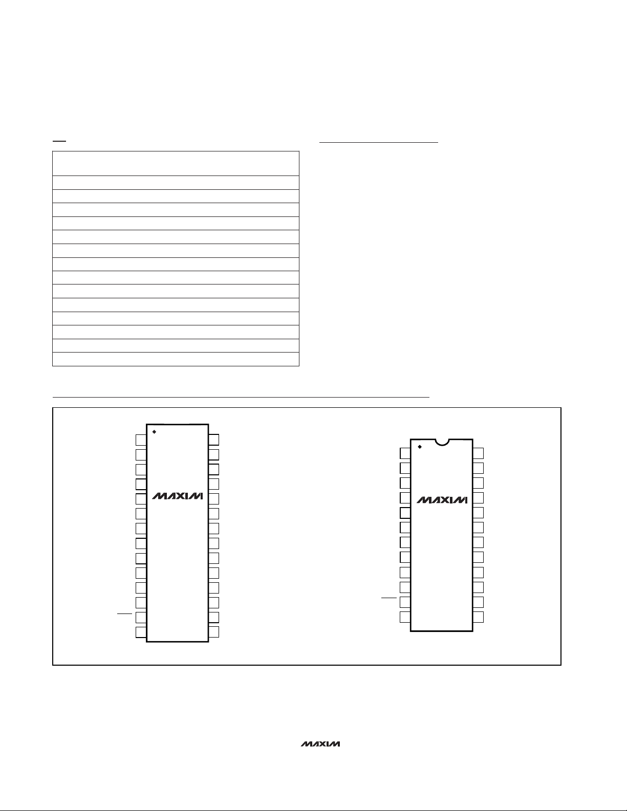
The MAX127/MAX128 are available in 24-pin DIP or
space-saving 28-pin SSOP packages.
Applications
Industrial Control Systems
Data-Acquisition Systems
Robotics
Automatic Testing
Battery-Powered Instruments
Medical Instruments
Features
♦ 12-Bit Resolution, 1/2 LSB Linearity
♦ +5V Single-Supply Operation
♦ I
2
C-Compatible, 2-Wire Serial Interface
♦ Four Software-Selectable Input Ranges
MAX127: 0 to +10V, 0 to +5V, ±10V, ±5V
MAX128: 0 to +V
REF
, 0 to +V
REF
/2, ±V
REF
,
±V
REF
/2
♦ 8 Analog Input Channels
♦ 8ksps Sampling Rate
♦ ±16.5V Overvoltage-Tolerant Input Multiplexer
♦ Internal 4.096V or External Reference
♦ Two Power-Down Modes
♦ 24-Pin Narrow DIP or 28-Pin SSOP Packages
EVALUATION KIT
AVAILABLE
For free samples & the latest literature: http://www.maxim-ic.com, or phone 1-800-998-8800.
For small orders, phone 408-737-7600 ext. 3468.
MAX127/MAX128
Multirange, +5V, 12-Bit DAS with
2-Wire Serial Interface
________________________________________________________________
Maxim Integrated Products
1
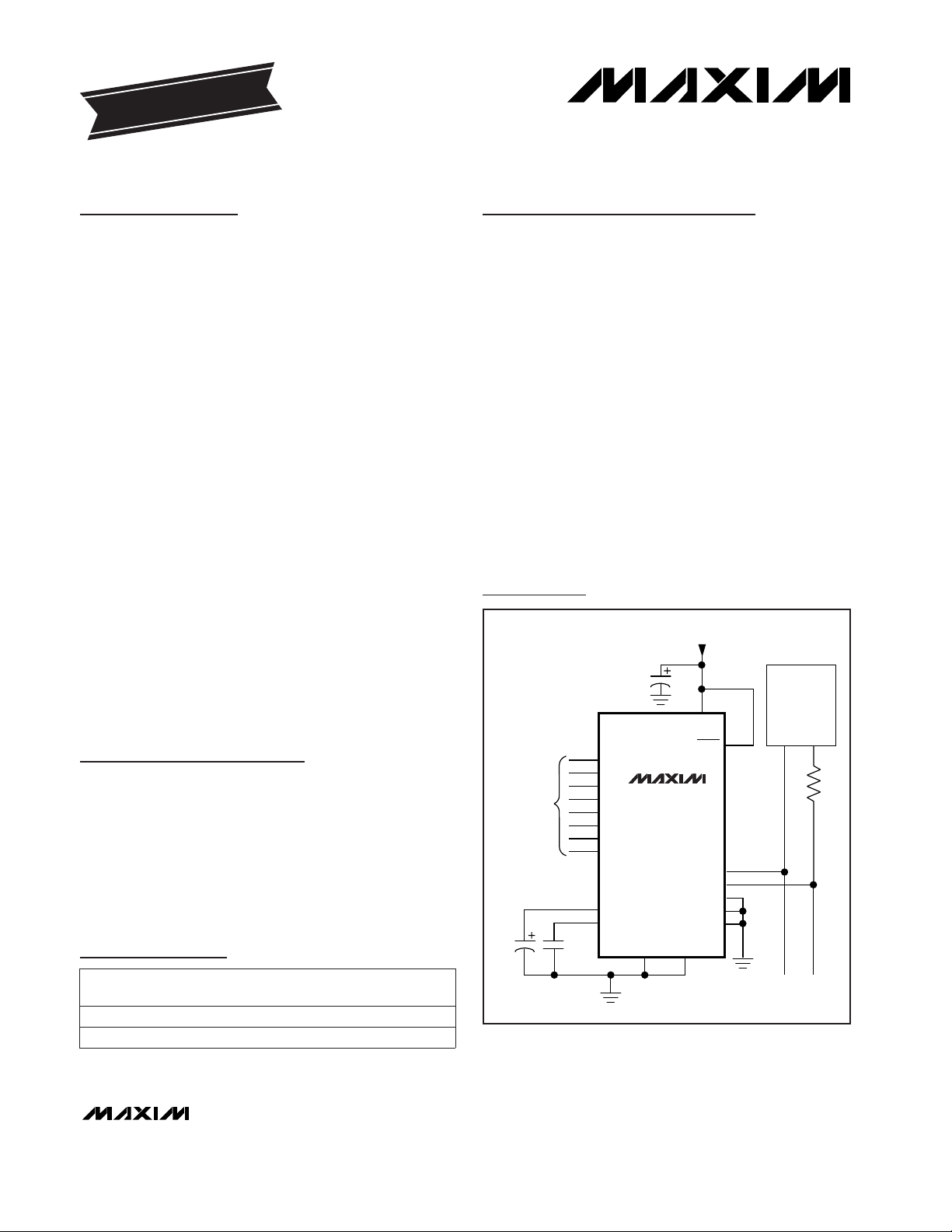
V
DD
CH0
CH1
CH2
CH3
CH4
CH5
CH6
CH7
DGND
0.01µF
µC
4.7µF
0.1µF
1k
SHDN
MAX127
MAX128
+5V
ANALOG
INPUTS
SCL
SDA
A0
A1
A2
REF
REFADJ
AGND
SCL SDA
Typical Operating Circuit
19-4773; Rev 0; 7/98
Ordering Information continued at end of data sheet.
PART
MAX127ACNG
MAX127ACNG 0°C to +70°C
0°C to +70°C
TEMP. RANGE PIN-PACKAGE
24 Narrow Plastic DIP
24 Narrow Plastic DIP ±1
±1/2
INL
(LSB)
Pin Configurations appear at end of data sheet.
Ordering Information
Page 2
MAX127/MAX128
Multirange, +5V, 12-Bit DAS with
2-Wire Serial Interface
2 _______________________________________________________________________________________
ABSOLUTE MAXIMUM RATINGS
Stresses beyond those listed under “Absolute Maximum Ratings” may cause permanent damage to the device. These are stress ratings only, and functional
operation of the device at these or any other conditions beyond those indicated in the operational sections of the specifications is not implied. Exposure to
absolute maximum rating conditions for extended periods may affect device reliability.
VDDto AGND............................................................-0.3V to +6V
AGND to DGND.....................................................-0.3V to +0.3V
CH0–CH7 to AGND ......................................................... ±16.5V
REF to AGND..............................................-0.3V to (V
DD
+ 0.3V)
REFADJ to AGND.......................................-0.3V to (V
DD
+ 0.3V)
A0, A1, A2 to DGND...................................-0.3V to (V
DD
+ 0.3V)
SHDN, SCL, SDA to DGND......................................-0.3V to +6V
Max Current into Any Pin ....................................................50mA
Continuous Power Dissipation (T
A
= +70°C)
24-Pin Narrow DIP (derate 13.33mW/°C above +70°C)..1067mW
28-Pin SSOP (derate 9.52mW/°C above +70°C)...............762mW
Operating Temperature Ranges
MAX127_ C_ _/MAX128_ C_ _.............................0°C to +70°C
MAX127_ E_ _/MAX128_ E_ _ ..........................-40°C to +85°C
Storage Temperature Range ............................-65°C to +150°C
Lead Temperature (soldering, 10sec) ............................+300°C
MAX127A/MAX128A
4kHz, VIN= ±5V (Note 3)
Up to the 5th harmonic
Bipolar
MAX127B/MAX128B
Unipolar
CONDITIONS
10Aperture Jitter
ns200Aperture Delay
dB
-86
Channel-to-Channel Crosstalk
dB81SFDRSpurious-Free Dynamic Range
dB-87 -80THDTotal Harmonic Distortion
dB70
LSB
±1/2
INLIntegral Nonlinearity
Bits12Resolution
±0.3
LSB
±0.1
Channel-to-Channel Offset
Error Matching
±10
±5
±1
LSB±1DNLDifferential Nonlinearity
LSB
±3
Offset Error
±5
UNITSMIN TYP MAXSYMBOLPARAMETER
Bipolar
Unipolar
5
ppm/°C
3
Gain Tempco (Note 2)
±10
±7
LSB
±7
Gain Error (Note 2)
±10
SINAD
Signal-to-Noise plus Distortion
Ratio
ns
Bipolar
Unipolar
Bipolar
MAX127B/MAX128B
MAX127B/MAX128B
Unipolar
MAX127B/MAX128B
MAX127B/MAX128B
MAX127A/MAX128A
MAX127A/MAX128A
MAX127A/MAX128A
MAX127A/MAX128A
ELECTRICAL CHARACTERISTICS
(VDD= +5V ±5%; unipolar/bipolar range; external reference mode, V
REF
= 4.096V; 4.7µF at REF; external clock, f
CLK
= 400kHz;
T
A
= T
MIN
to T
MAX
; unless otherwise noted. Typical values are at TA= +25°C.)
DYNAMIC SPECIFICATIONS (800Hz sine-wave input, ±10Vp-p (MAX127) or ±4.096Vp-p (MAX128), f
SAMPLE
= 8ksps)
DC, VIN= ±16.5V -96
ACCURACY (Note 1)
Page 3
MAX127/MAX128
Multirange, +5V, 12-Bit DAS with
2-Wire Serial Interface
_______________________________________________________________________________________ 3
ELECTRICAL CHARACTERISTICS (continued)
(VDD= +5V ±5%; unipolar/bipolar range; external reference mode, V
REF
= 4.096V; 4.7µF at REF pin; external clock, f
CLK
= 400kHz;
T
A
= T
MIN
to T
MAX
; unless otherwise noted. Typical values are at TA= +25°C.)
MAX128
MAX127
MAX127
-600 360
I
IN
-1200 720
µA
±V
REF
/2 range
±V
REF
range
±5V range
-1200 10
±10V range
-600 10
Bipolar
Input Voltage Range V
IN
-10 10
TC V
REF
-5 5
MAX127
-V
REF
V
REF
-V
REF
/2 V
REF
/2
MAX128
Bipolar,
Table 3
MAX127
MAX128
0 to 5V or 0 to V
REF
/2 range
0 to 10V or 0 to V
REF
range
±5V or ±V
REF
/2 range
±10V or ±V
REF
range
Buffer Voltage Gain 1.638 V/V
REFADJ Adjustment Range ±1.5 %Figure 12
Capacitive Bypass at REF 4.7 µF
REFADJ Output Voltage 2.465 2.500 2.535 V
Load Regulation (Note 5) 10 mV0 to 0.5mA output current
0 V
REF
0 V
REF
/2
Unipolar,
Table 3
Input Resistance
∆V
IN
∆I
IN
21
kΩ
16
-10 360
Unipolar
Input Current
-10 720
Bipolar
MAX128
0 to 5V range
-10 0.1 10
0 to 10V range
Unipolar
2.5
Small-Signal Bandwidth
5
MHz
PARAMETER SYMBOL MIN TYP MAX UNITS
2.5
-3dB
rolloff
1.25
0 10
V
0 5
Track/Hold Acquisition Time 3 µs
Input Capacitance 40 pF
REFOUT Voltage V
REF
4.076 4.096 4.116 V
REFOUT Tempco
±15
ppm/°C
Output Short-Circuit Current 30 mA
CONDITIONS
(Note 4)
TA= +25°C
MAX127_C/MAX128_C
±30MAX127_E/MAX128_E
ANALOG INPUT
INTERNAL REFERENCE
Page 4
MAX127/MAX128
Multirange, +5V, 12-Bit DAS with
2-Wire Serial Interface
4 _______________________________________________________________________________________
ELECTRICAL CHARACTERISTICS (continued)
(VDD= +5V ±5%; unipolar/bipolar range; external reference mode, V
REF
= 4.096V; 4.7µF at REF pin; external clock, f
CLK
= 400kHz;
T
A
= T
MIN
to T
MAX
; unless otherwise noted. Typical values are at TA= +25°C.)
V2.4 4.18Input Voltage Range
VVDD- 0.5
REFADJ Threshold for
Buffer Disable
Normal or STANDBY power-down mode kΩ10
Input Resistance
FULL power-down mode 5 MΩ
External reference = 4.096V
CONDITIONS
FULL power-down mode
LSB
±0.1 ±0.5
PSRR
Power-Supply Rejection Ratio
(Note 7)
µs
V4.75 5.25V
DD
Supply Voltage
6.0 7.7 10.0t
CONV
Conversion Time
120 220
Normal mode, bipolar ranges
700 850
Normal mode, unipolar ranges
UNITSMIN TYP MAXSYMBOLPARAMETER
STANDBY power-down mode (Note 6)
mA
18
I
DD
Supply Current
6 10
µA
Internal reference ±0.5
0.4f
CLK
External Clock Frequency Range MHz
Power-up (Note 8) µs200
Bandgap Reference
Start-Up Time
ksps8Throughput Rate
C
IN
15 pF(Note 4)
Input Leakage Current I
IN
±0.1 ±10 µAVIN= 0 or V
DD
Input Low Threshold Voltage V
IL
0.8 V
Input High Threshold Voltage V
IH
2.4 V
Input Capacitance
V
HYS
0.2 VInput Hysteresis
400
V
REF
=
4.18V
µA
1
Input Current
FULL power-down mode
Normal, or STANDBY
power-down mode
To 0.1mV, REF bypass
capacitor fully discharged
ms
8
Reference Buffer Settling Time
POWER REQUIREMENTS
TIMING
REFERENCE INPUT (buffer disabled, reference input applied to REF)
DIGITAL INPUTS (SHDN, A2, A1, A0)
C
REF
= 4.7µF
C
REF
= 33µF 60
Page 5
MAX127/MAX128
Multirange, +5V, 12-Bit DAS with
2-Wire Serial Interface
_______________________________________________________________________________________ 5
ELECTRICAL CHARACTERISTICS (continued)
(VDD= +5V ±5%; unipolar/bipolar range; external reference mode, V
REF
= 4.096V; 4.7µF at REF pin; external clock, f
CLK
= 400kHz;
T
A
= T
MIN
to T
MAX
; unless otherwise noted. Typical values are at TA= +25°C.)
Input Hysteresis V
HYS
0.05 x V
DD
V
Input Low Threshold Voltage V
IL
0.3 x V
DD
V
Input High Threshold Voltage V
IH
0.7 x V
DD
V
PARAMETER SYMBOL MIN TYP MAX UNITSCONDITIONS
TIMING CHARACTERISTICS
(VDD= +4.75V to +5.25V; unipolar/bipolar range; external reference mode, V
REF
= 4.096V; 4.7µF at REF pin; TA= T
MIN
to T
MAX
;
unless otherwise noted. Typical values are at T
A
= +25°C.)
Input Capacitance C
IN
15 pF
Page 6
MAX127/MAX128
Multirange, +5V, 12-Bit DAS with
2-Wire Serial Interface
6 _______________________________________________________________________________________
TIMING CHARACTERISTICS (continued)
(VDD= +4.75V to +5.25V; unipolar/bipolar range; external reference mode, V
REF
= 4.096V; 4.7µF at REF pin; TA = T
MIN
to T
MAX;
unless otherwise noted. Typical values are at TA = +25°C.)
Note 1: Accuracy specifications tested at V
DD
= 5.0V. Performance at power-supply tolerance limits is guaranteed by Power-
Supply Rejection test.
Note 2: External reference: V
REF
= 4.096V, offset error nulled, ideal last-code transition = FS - 3/2LSB.
Note 3: Ground “on” channel, sine wave applied to all “off” channels.
Note 4: Guaranteed by design. Not tested.
Note 5: Use static external load during conversion for specified accuracy.
Note 6: Tested using internal reference.
Note 7: PSRR measured at full scale. Tested for the ±10V (MAX127) and ±4.096V (MAX128) input ranges.
Note 8: Not subject to production testing. Provided for design guidance only.
PARAMETERS SYMBOL MIN TYP MAX UNITSCONDITIONS
Low Period of the SCL Clock t
LOW
4.7 µs
High Period of the SCL Clock t
HIGH
4.0 µs
Setup Time for a Repeated
START Condition
t
SU, STA
4.7 µs
Data Hold Time t
HD, DAT
0 0.9 µs
Data Setup Time t
SU, DAT
250 ns
Rise Time for Both SDA and SCL
Signals (Receiving)
t
R
1000 ns
Fall Time for Both SDA and SCL
Signals (Receiving)
t
F
300 ns
Fall Time for Both SDA and SCL
Signals (Transmitting)
t
F
Cb = total capacitance of one bus line in pF,
up to 6mA sink
20 + 250
0.1 x C
b
ns
Setup Time for STOP Condition t
SU, STO
4.0 µs
Capacitive Load for Each
Bus Line
C
b
400 pF
Pulse Width of Spike Suppressed t
SP
0 50 ns
Hold Time (Repeated) START
Condition
t
HD,STA
4.0 µs
Bus Free Time Between a STOP
and START Condition
t
BUF
4.7 µs
SCL Clock Frequency f
SCL
100 kHz
2-WIRE STANDARD MODE
Page 7

MAX127/MAX128
Multirange, +5V, 12-Bit DAS with
2-Wire Serial Interface
_______________________________________________________________________________________
7
0
5
15
10
20
25
0 21 3 4 5 6 7
SUPPLY CURRENT vs. SUPPLY VOLTAGE
max127/8-01
SUPPLY VOLTAGE (V)
SUPPLY CURRENT (mA)
Page 8

MAX127/MAX128
Multirange, +5V, 12-Bit DAS with
2-Wire Serial Interface
8 _______________________________________________________________________________________
Pin Description
PIN
NAME FUNCTION
DIP SSOP
1, 2 1, 2 V
DD
+5V Supply. Bypass with a 0.1µF capacitor to AGND.
3, 9, 22, 24
4, 7, 8, 11, 22,
24, 25, 28
N.C. No Connect. No internal connection.
4 3 DGND Digital Ground
5 5 SCL Serial Clock Input
6, 8, 10 6, 10, 12 A0, A2, A1 Address Select Inputs
7 9 SDA
Open-Drain Serial Data I/O. Input data is clocked in on the rising edge of SCL,
and output data is clocked out on the falling edge of SCL. External pull-up
resistor required.
11 13
SHDN
Shutdown Input. When low, device is in full power-down (FULLPD) mode.
Connect high for normal operation.
12 14 AGND Analog Ground
13–20 15–21, 23 CH0–CH7 Analog Input Channels
21 26 REFADJ
Bandgap Voltage-Reference Output/External Adjust Pin. Bypass with a 0.01µF
capacitor to AGND. Connect to VDDwhen using an external reference at REF.
23 27 REF
Reference Buffer Output/ADC Reference Input. In internal reference mode, the
reference buffer provides a 4.096V nominal output, externally adjustable at
REFADJ. In external reference mode, disable the internal reference by pulling
REFADJ to VDDand applying the external reference to REF.
Page 9
MAX127/MAX128
Multirange, +5V, 12-Bit DAS with
2-Wire Serial Interface
_______________________________________________________________________________________ 9
Detailed Description
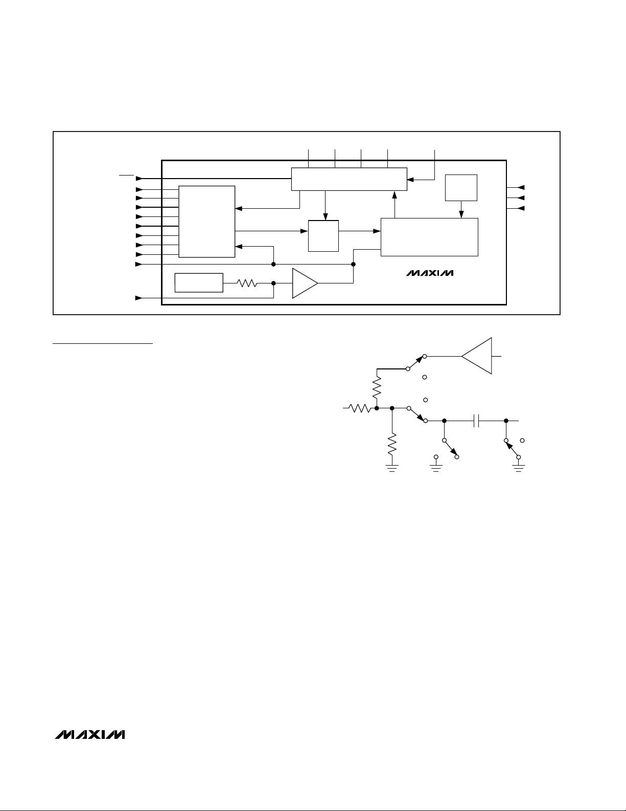
Converter Operation
The MAX127/MAX128 multirange, fault-tolerant ADCs
use successive approximation and internal track/hold
(T/H) circuitry to convert an analog signal to a 12-bit
digital output. Figure 1 shows the block diagram for
these devices.
Analog-Input Track/Hold
The T/H circuitry enters its tracking/acquisition mode on
the falling edge of the sixth clock in the 8-bit input control word and enters its hold/conversion mode when the
master issues a STOP condition. For timing information,
see the
Start a Conversion
section.
Input Range and Protection
The MAX127/MAX128 have software-selectable input
ranges. Each analog input channel can be independently programmed to one of four ranges by setting the
appropriate control bits (RNG, BIP) in the control byte
(Table 1). The MAX127 has selectable input ranges
extending to ±10V (±V
REF
x 2.441), while the MAX128
has selectable input ranges extending to ±V
REF
. Note
that when an external reference is applied at REFADJ,
the voltage at REF is given by V
REF
= 1.638 x V
REFADJ
(2.4 < V
REF
< 4.18). Figure 2 shows the equivalent
input circuit.
A resistor network on each analog input provides a
±16.5V fault protection for all channels. This circuit limits the current going into or out of the pin to less than
1.2mA, whether or not the channel is on. This provides
an added layer of protection when momentary overvoltages occur at the selected input channel, and when
a negative signal is applied at the input even though
the device may be configured for unipolar mode.
Overvoltage protection is active even if the device is in
power-down mode or V
DD
= 0.
Digital Interface
The MAX127/MAX128 feature a 2-wire serial interface
consisting of the SDA and SCL pins. SDA is the data
I/O and SCL is the serial clock input, controlled by the
master device. A2–A0 are used to program the
MAX127/MAX128 to different slave addresses. (The
MAX127/MAX128 only work as slaves.) The two bus
lines (SDA and SCL) must be high when the bus is not
in use. External pull-up resistors (1kΩor greater) are
required on SDA and SCL to maintain I2C compatibility.
Table 1 shows the input control-byte format.
Figure 1. Block Diagram
CH2
CH1
CH0
SHDN
CH3
CH4
CH5
CH6
CH7
REFADJ
REF
V
DD
AGND
DGND
MAX127
MAX128
12-BIT SAR ADC
IN
REF
CLOCK
OUT
T/H
2.5V
REFERENCE
ANALOG
INPUT
MUX
AND SIGNAL
CONDITIONING
AV =
1.638
INT
CLOCK
SDA
A2 A1 A0 SCL
SERIAL INTERFACE LOGIC
10k
Figure 2. Equivalent Input Circuit
5.12k
Page 10

MAX127/MAX128
Multirange, +5V, 12-Bit DAS with
2-Wire Serial Interface
10 ______________________________________________________________________________________
BIT 7
(MSB)
BIT 6 BIT 5 BIT 4 BIT 3 BIT 2 BIT 1
BIT 0
(LSB)
START SEL2 SEL1 SEL0 RNG BIP PD1 PD0
Table 1. Control-Byte Format
BIT NAME DESCRIPTION
7 (MSB) START
The logic "1" received after acknowledge of a write bit (R/W = 0) defines the
beginning of the control byte.
6, 5, 4
SEL2, SEL1,
SEL0
These three bits select the desired "ON" channel (Table 2).
3 RNG
Selects the full-scale input voltage range (Table 3).
2 BIP
Selects unipolar or bipolar conversion mode (Table 3).
1, 0 (LSB) PD1, PD0
These two bits select the power-down modes (Table 4).
SEL2 SEL1 SEL0 CHANNEL
0 0 0 CH0
0 0 1 CH1
0 1 0 CH2
0 1 1 CH3
1 0 0 CH4
1 0 1 CH5
1 1 0 CH6
1 1 1 CH7
Table 2. Channel Selection
Table 3. Range and Polarity Selection
INPUT RANGE (V) RNG BIP
NEGATIVE FULL
SCALE (V)
ZERO
SCALE (V)
FULL SCALE (V)
0 to 5 0 0 – 0 V
REF
x 1.2207
0 to 10 1 0 – 0 V
REF x 2.4414
±5 0 1 -V
REF
x 1.2207 0 V
REF
x 1.2207
±10 1 1 -V
REF x 2.4414
0 V
REF x 2.4414
Table 4. Power-Down and Clock
Selection
PD1 PD0 MODE
0 X Normal Operation (always on)
1 0 Standby Power-Down Mode (STBYPD)
1 1 Full Power-Down Mode (FULLPD)
0 to V
REF
1 0 – 0 V
REF
±V
REF
/2 0 1 -V
REF
/2 0 V
REF
/2
±V
REF
1 1 -V
REF
0 V
REF
0 to V
REF
/2 0 0 – 0 V
REF
/2
MAX127
MAX128
Page 11

Slave Address
The MAX127/MAX128 have a 7-bit-long slave address.
The first four bits (MSBs) of the slave address have
been factory programmed and are always 0101. The
logic state of the address input pins (A2–A0) determine
the three LSBs of the device address (Figure 3). A maximum of eight MAX127/MAX128 devices can therefore
be connected on the same bus at one time.
A2–A0 may be connected to VDDor DGND, or they
may be actively driven by TTL or CMOS logic levels.
The eighth bit of the address byte determines whether
the master is writing to or reading from the MAX127/
MAX128 (R/W = 0 selects a write condition. R/W = 1
selects a read condition).
Conversion Control
The master signals the beginning of a transmission with
a START condition (S), which is a high-to-low transition
on SDA while SCL is high. When the master has finished communicating with the slave, the master issues
a STOP condition (P), which is a low-to-high transition
on SDA while SCL is high (Figure 4). The bus is then
free for another transmission. Figure 5 shows the timing
diagram for signals on the 2-wire interface. The
address-byte, control-byte, and data-byte are transmitted between the START and STOP conditions. The SDA
state is allowed to change only while SCL is low, except
for the START and STOP conditions. Data is transmitted
in 8-bit words. Nine clock cycles are required to transfer the data in or out of the MAX127/MAX128. (Figures
9 and 10).
MAX127/MAX128
Multirange, +5V, 12-Bit DAS with
2-Wire Serial Interface
______________________________________________________________________________________ 11
SCL
SDA
SLAVE ADDRESS BITS A2, A1, AND A0 CORRESPOND TO THE LOGIC STATE
OF THE ADDRESS INPUT PINS A2, A1, AND A0.
00 1 A21 R/WA1 A0
LSB
ACK
SLAVE ADDRESS
Figure 3. Address Byte
SCL
SDA
t
LOW
t
HIGH
t
F
t
R
tHD,
STA
tHD,
DAT
tHD,
STA
tSU,
DAT
tSU,
STA
t
BUF
tSU,
STO
START CONDITIONSTOP CONDITIONREPEATED START CONDITIONSTART CONDITION
Figure 5. 2-Wire Serial-Interface Timing Diagram
SCL
SDA
START CONDITION
STOP CONDITION
Figure 4. START and STOP Conditions
Page 12

MAX127/MAX128
Start a Conversion (Write Cycle)
A conversion cycle begins with the master issuing a
START condition followed by seven address bits
(Figure 3) and a write bit (R/W = 0). Once the eighth bit
has been received and the address matches, the
MAX127/MAX128 (the slave) issues an acknowledge
by pulling SDA low for one clock cycle (A = 0). The
master then writes the input control byte to the slave
(Figure 8). After this byte of data, the slave issues
another acknowledge, pulling SDA low for one clock
cycle. The master ends the write cycle by issuing a
STOP condition (Figure 6).
When the write bit is set (R/W = 0), acquisition starts as
soon as Bit 2 (BIP) of the input control-byte has been
latched and ends when a STOP condition has been
issued. Conversion starts immediately after acquisition.
The MAX127/MAX128’s internal conversion clock frequency is 1.56MHz, resulting in a typical conversion
time of 7.7µs. Figure 9 shows a complete write cycle.
Read a Conversion (Read Cycle)
Once a conversion starts, the master does not need to
wait for the conversion to end before attempting to read
the data from the slave. Data access begins with the
master issuing a START condition followed by a 7-bit
address (Figure 3) and a read bit (R/W = 1). Once the
eighth bit has been received and the address matches,
the slave issues an acknowledge by pulling low on SDA
for one clock cycle (A = 0) followed by the first byte of
serial data (D11–D4, MSB first). After the first byte has
been issued by the slave, it releases the bus for the
master to issue an acknowledge (A = 0). After receiving the acknowledge, the slave issues the second byte
(D3–D0 and four zeros) followed by a NOT acknowledge (A= 1) from the master to indicate that the last
data byte has been received. Finally, the master issues
a STOP condition (P), ending the read cycle (Figure 7).
Multirange, +5V, 12-Bit DAS with
2-Wire Serial Interface
12 ______________________________________________________________________________________
LSBMSB
SDA
SCL
START SEL2 SEL1 SEL0 RNG BIP PD1 PD0 ACK
START: FIRST LOGIC “1” RECEIVED AFTER ACKNOWLEDGE OF A WRITE.
ACK: ACKNOWLEDGE BIT. THE MAX127/MAX128 PULL SDA LOW DURING THE
9TH CLOCK PULSE.
Figure 8. Command Byte
Figure 9. Complete 2-Wire Serial Write Transmission
START
CONDITION
STOP
CONDITION
CONTROL BYTESLAVE ADDRESS BYTE
SCL
A/D STATE
SDA
MSB MSBLSB LSB
W
1 2 7 8 9 10 11 15 16 17 18
BIPS
10
PD1 PD0 AA
ACQUISITION CONVERSION
MASTER TO SLAVE
SLAVE TO MASTER
NO. OF BITS
S SLAVE ADDRESS W A CONTROL-BYTE A P
1 7 1 1 8 1 1
START CONDITION
WRITE
ACKNOWLEDGE
ACKNOWLEDGE
STOP CONDITION
Figure 6. Write Cycle
Figure 7. Read Cycle
1 7 1 1 8 1
S SLAVE ADDRESS R A DATA-BYTE A
START CONDITION
ACKNOWLEDGE
READ
8 1 1
DATA-BYTE A P
NOT ACKNOWLEDGE
MASTER TO SLAVE
SLAVE TO MASTER
NO. OF BITS
STOP CONDITION
Page 13

The MAX127/MAX128 ignore acknowledge and NOTacknowledge conditions issued by the master during
the read cycle. The device waits for the master to read
the output data or waits until a STOP condition is
issued. Figure 10 shows a complete read cycle.
In unipolar input mode, the output is straight binary. For
bipolar input mode, the output is two’s complement. For
output binary codes see the
Transfer Function
section.
Applications Information
Power-On Reset
The MAX127/MAX128 power up in normal operating
mode, waiting for a START condition followed by the
appropriate slave address. The contents of the input
and output data registers are cleared at power-up.
Internal or External Reference
The MAX127/MAX128 operate with either an internal or
an external reference (Figures 11a–11c). An external
reference is connected to either REF or to REFADJ.
The REFADJ internal buffer gain is trimmed to 1.6384 to
provide 4.096V at REF from a 2.5V reference.
Internal Reference
The internally trimmed 2.50V reference is amplified
through the REFADJ buffer to provide 4.096V at REF.
Bypass REF with a 4.7µF capacitor to AGND and bypass
REFADJ with a 0.01µF capacitor to AGND (Figure 11a).
The internal reference voltage is adjustable to ±1.5%
(±65 LSBs) with the reference-adjust circuit of Figure 12.
External Reference
To use the REF input directly, disable the internal buffer
by connecting REFADJ to V
DD
(Figure 11b). Using the
REFADJ input eliminates the need to buffer the reference externally. When the reference is applied at
REFADJ, bypass REFADJ with a 0.01µF capacitor to
AGND (Figure 11c).
At REF and REFADJ, the input impedance is a minimum of 10kΩ for DC currents. During conversions, an
external reference at REF must be able to drive a
400µA DC load, and must have an output impedance
of 10Ω or less. If the reference has higher input impedance or is noisy, bypass REF with a 4.7µF capacitor to
AGND as close to the chip as possible.
With an external reference voltage of less than 4.096V
at REF or less than 2.5V at REFADJ, the increase in
RMS noise to the LSB value (full-scale voltage/4096)
results in performance degradation and loss of effective bits.
Power-Down Mode
To save power, put the converter into low-current shutdown mode between conversions. Two programmable
power-down modes are available, in addition to the
hardware shutdown. Select STBYPD or FULLPD by programming PD0 and PD1 in the input control byte (Table
4). When software power-down is asserted, it becomes
effective only after the end of conversion. In all powerdown modes, the interface remains active and conversion results may be read. Input overvoltage protection
is active in all power-down modes.
MAX127/MAX128
Multirange, +5V, 12-Bit DAS with
2-Wire Serial Interface
______________________________________________________________________________________ 13
Figure 10. Complete 2-Wire Serial Read Transmission
START
CONDITION
STOP
CONDITION
LSB DATA BYTEMSB DATA BYTE
SLAVE ADDRESS BYTE
MSB MSB
MSB
LSB LSB LSB
0 1
1 2 7 8 9 10 11 17 18 19 22 23 26 27
R
A D11 D4 A D3 D0 A
FILLED WITH
4 ZEROS
Page 14

MAX127/MAX128
To power-up from a software initiated power-down, a
START condition followed by the correct slave address
must be received (with R/W = 0). The MAX127/MAX128
power-up after receiving the next bit.
For hardware-controlled power-down (FULLPD), pull
SHDN low. When hardware shutdown is asserted, it
becomes effective immediately and any conversion in
progress is aborted.
Choosing Power-Down Modes
The bandgap reference and reference buffer remain
active in STBYPD mode, maintaining the voltage on the
4.7µF capacitor at REF. This is a “DC” state that does
not degrade after standby power-down of any duration.
In FULLPD mode, only the bandgap reference is active.
Connect a 33µF capacitor between REF and AGND to
maintain the reference voltage between conversions
and to reduce transients when the buffer is enabled
and disabled. Throughput rates down to 1ksps can be
achieved without allotting extra acquisition time for reference recovery prior to conversion. This allows conversion to begin immediately after power-down ends. If
the discharge of the REF capacitor during FULLPD
exceeds the desired limits for accuracy (less than a
fraction of an LSB), run a STBYPD power-down cycle
prior to starting conversions. Take into account that the
reference buffer recharges the bypass capacitor at an
80mV/ms slew rate, and add 50µs for settling time.
Auto-Shutdown
Selecting STBYPD on every conversion automatically
shuts the MAX127/MAX128 down after each conversion
without requiring any start-up time on the next conversion.
Multirange, +5V, 12-Bit DAS with
2-Wire Serial Interface
14 ______________________________________________________________________________________
REF
10k
2.5V
C
REF
4.7µF
2.5V
REFADJ
A
V
= 1.638
0.01µF
MAX127
MAX128
Figure 11c. External Reference, Reference at REFADJ
100k
510k
24k
REFADJ
+5V
0.01µF
MAX127
MAX128
Figure 12. Reference-Adjust Circuit
REF
10k
2.5V
C
REF
4.7µF
0.01µF
REFADJ
A
V
= 1.638
MAX127
MAX128
Figure 11a. Internal Reference
REF
V
DD
10k
2.5V
4.096V
C
REF
4.7µF
REFADJ
A
V
= 1.638
MAX127
MAX128
Figure 11b. External Reference, Reference at REF
Page 15

Transfer Function
Output data coding for the MAX127/MAX128 is binary
in unipolar mode with 1LSB = (FS/4096) and
two’s complement binary in bipolar mode with 1LSB =
[(2 x|FS|) /4096]. Code transitions occur halfway
between successive-integer LSB values. Figures 13a
and 13b show the input/output (I/O) transfer functions
for unipolar and bipolar operations, respectively. For
full-scale (FS) values, refer to Table 3.
Layout, Grounding, and Bypassing
Careful printed circuit board layout is essential for best
system performance. For best performance, use a
ground plane. To reduce crosstalk and noise injection,
keep analog and digital signals separate. Connect analog grounds and DGND in a star configuration to
AGND. For noise-free operation, ensure the ground
return from AGND to the supply ground is low impedance and as short as possible. Connect the logic
grounds directly to the supply ground. Bypass V
DD
with
0.1µF and 4.7µF capacitors to AGND to minimize highand low-frequency fluctuations. If the supply is excessively noisy, connect a 5Ω resistor between the supply
and VDD, as shown in Figure 14.
MAX127/MAX128
Multirange, +5V, 12-Bit DAS with
2-Wire Serial Interface
______________________________________________________________________________________ 15
OUTPUT CODE
INPUT VOLTAGE (LSB)
0
FS
FS -
3
/2 LSB
1 LSB =
FULL-SCALE
TRANSITION
1 2 3
11... 111
11... 110
11... 101
00... 011
00... 010
00... 001
00... 000
FS
4096
Figure 13a. Unipolar Transfer Function
OUTPUT CODE
INPUT VOLTAGE (LSB)
0 +FS - 1 LSB
1 LSB =
-FS
011... 111
011... 110
000... 001
000... 000
111... 111
100... 010
100... 001
100... 000
2FS
4096
Figure 13b. Bipolar Transfer Function
V
DD
GND
DGND
DGNDAGND
+5V
+5V
SUPPLY
R* = 5Ω
DIGITAL
CIRCUITRY
4.7µF
0.1µF
MAX127
MAX128
**
* OPTIONAL
** CONNECT AGND AND DGND WITH A GROUND PLANE OR A SHORT TRACE.
Figure 14. Power-Supply Grounding Connection
Page 16
28
27
26
25
24
23
22
21
20
19
18
17
16
15
1
2
3
4
5
6
7
8
9
10
11
12
13
14
N.C.
REF
REFADJ
N.C.
N.C.
CH7
CH0
N.C.
CH6
CH5
CH4
CH3
CH2
CH1
AGND
SHDN
A1
N.C.
A2
SDA
N.C.
N.C.
A0
SCL
N.C.
DGND
V
DD
V
DD
SSOP
TOP VIEW
MAX127
MAX128
MAX127/MAX128
Multirange, +5V, 12-Bit DAS with
2-Wire Serial Interface
Maxim cannot assume responsibility for use of any circuitry other than circuitry entirely embodied in a Maxim product. No circuit patent licenses are
implied. Maxim reserves the right to change the circuitry and specifications without notice at any time.
16
____________________Maxim Integrated Products, 120 San Gabriel Drive, Sunnyvale, CA 94086 408-737-7600
© 1998 Maxim Integrated Products Printed USA is a registered trademark of Maxim Integrated Products.
24
23
22
21
20
19
18
17
1
2
3
4
5
6
7
8
N.C.
REF
N.C.
REFADJDGND
N.C.
V
DD
V
DD
CH7
CH6
CH5
CH4A2
SDA
A0
SCL
16
15
14
13
9
10
11
12
CH3
CH2
CH1
CH0AGND
SHDN
A1
N.C.
DIP
MAX127
MAX128
Pin Configurations
Ordering Information (continued)
Chip Information
TRANSISTOR COUNT: 4219
SUBSTRATE CONNECTED to AGND
PART
MAX127ACAI
MAX127BCAI 0°C to +70°C
0°C to +70°C
TEMP. RANGE PIN-PACKAGE
28 SSOP
28 SSOP ±1
±1/2
INL
(LSB)
MAX127AENG
MAX127BENG -40°C to +85°C
-40°C to +85°C 24 Narrow Plastic DIP
24 Narrow Plastic DIP ±1
±1/2
MAX127AEAI
MAX127BEAI -40°C to +85°C
-40°C to +85°C 28 SSOP
28 SSOP ±1
±1/2
MAX128ACNG
MAX128BCNG
MAX128ACAI
MAX128BCAI
0°C to +70°C
0°C to +70°C 24 Narrow Plastic DIP
24 Narrow Plastic DIP
0°C to +70°C
0°C to +70°C
±1
±1/2
28 SSOP
28 SSOP ±1
±1/2
MAX128AENG
MAX128BENG -40°C to +85°C
-40°C to +85°C 24 Narrow Plastic DIP
24 Narrow Plastic DIP ±1
±1/2
MAX128AEAI
MAX128BEAI -40°C to +85°C
-40°C to +85°C 28 SSOP
28 SSOP ±1
±1/2
 Loading...